
Gigantic enhancement of electricity generation in piezoelectric semiconductors by creating pores as a universal approach†
Yu-Lun
Su‡
a,
Kapil
Gupta‡
 a,
Yu-Liang
Hsiao
a,
Ruey-Chi
Wang
b and
Chuan-Pu
Liu
*ac
a,
Yu-Liang
Hsiao
a,
Ruey-Chi
Wang
b and
Chuan-Pu
Liu
*ac
aDepartment of Materials Science and Engineering, National Cheng Kung University, Tainan 701, Taiwan. E-mail: cpliu@mail.ncku.edu.tw
bDepartment of Chemical and Materials Engineering, National University of Kaohsiung, Kaohsiung 81148, Taiwan
cHierarchical Green-Energy Materials (Hi-GEM) Research Center, National Cheng Kung University, Tainan 701, Taiwan
First published on 12th December 2018
Abstract
In the Internet of Things era, both self-powered nanodevices and nanogenerators (NGs) that harvest energy from mechanical vibrations are highly attractive, prompting a rapid surge in research on enhancing their performance. We demonstrate a versatile approach for diverse materials, by altering the microstructure with discontinuous nano-pores in one-dimensional nanostructures, which can be readily extended to higher-dimensional single crystal materials, such as epitaxial thin films. This novel approach is demonstrated for two applications, direct-current (DC) NGs and piezotronics, by taking ZnO as a model, where remarkably enhanced performance is demonstrated in theoretical simulations and confirmed by experiments. Here, we report that porous ZnO nanowire based DC-NGs demonstrated ∼23 times enhancement of output performance, and strain-gated transistors exhibited ∼6 times enhancement of force sensitivity. This can potentially augment energy harvesting and pressure sensing for many applications, such as self-powered nano-devices and touch panels.
Broader contextOn a micro/nanoscale, upcoming multi-functional devices that are capable of sensing, controlling, communicating and actuating/responding (e.g., implantable biosensors, micro-electromechanical systems and portable/wearable personal electronics, etc.) will require sustainable and continuous operations with least possible power consumption. Thus, it is highly desirable to develop such multi-functional nanodevices, integrated into nanosystems, to be self-powered. Therefore, emerging technology that can harvest energy from the environment on the nanoscale is crucial. One such technique for self-powering nanodevices is to harvest energy from tiny random vibrations in the environment. Consequently, intensive studies on enhancing the performance of piezoelectric nanogenerators are currently being pursued, as they can convert nanoscale mechanical energy into electrical energy. In this paper, we demonstrate a versatile approach to significantly enhance supposedly an intrinsic property of piezoelectric semiconductor materials, i.e., piezoelectric potential, through theoretical simulations followed by experimental verification, where porous nanowire based nanogenerators exhibited ∼23 times enhancement of output performance. This approach can be widely applied to diverse materials, by altering the microstructure with discontinuous inner and surface nano-pores in one-dimensional nanostructures, and can be easily extended to higher-dimensional single crystal materials, such as epitaxial thin films. |
Introduction
Piezotronics holds a crucial position in the next generation self-powered nano-devices, including transistors, nanogenerators (NGs), photodetectors, and bio-sensors,1–13 certainly propelling toward the ages of the Internet of Things. Due to the non-central symmetric structure of wurtzite materials, external mechanical stress efficiently displaces the centers of positive and negative charges relative to each other, to form dipole moments. The superposition of all the dipole moments forms a considerable potential difference along the polarization direction, which is known as the piezoelectric potential (piezopotential). This strain-induced piezopotential is a well-known mechanism behind energy harvesting, as it serves as a driving force for the current flow across a load when a conductive atomic force microscope (C-AFM) metal tip scans over a nanowire (NW). Due to the characteristics of the Schottky contact at the AFM tip–ZnO NW interface, a dc current can be generated under forward-bias conditions, which are established through a negative piezopotential as the external bias when the AFM tip touches the compressed side of the NW.2 By combining semiconductor properties and the piezoelectric effect, in the context of piezotronics, the emerging piezopotential can effectively tune the Schottky barrier height (SBH) at the interfaces of the devices, which is critical for controlling carrier transport in various electronic devices.In order to enhance the performances of piezotronic devices and NGs, a search for new materials with higher piezoelectric coefficients has become the most straightforward approach.14 However, development of new materials is often hindered by the available synthesis techniques, let alone to compete with traditional materials used in fabricating large-scale high-quality nanodevices. Alternatively, it may be more beneficial and cost-effective if the piezoelectric properties of a given material could be enhanced simply by altering the microstructure itself. From the aspects of microstructure, several strategies have been demonstrated to improve the performances of piezotronics and NGs, including the aspect ratio of nanowires (NWs),15–17 doping,18–24 and orientation of oblique-aligned NWs.25,26 Furthermore, functionalization and decoration, such as Au nanoparticles, have been used to enhance the strain sensitivity of single NW based strain-gated transistors (SGTs) via a coupling effect of piezopotential and localized Schottky barriers (SBs).4,5,27 However, these approaches are limited to specific materials, preventing them from universal implementation. In this paper, we propose a facile versatile approach, i.e., modification of the microstructure using discontinuous inner and surface nano-pores in piezoelectric semiconductor NWs, demonstrated by theoretical simulations accompanied by outstanding experimental results, using ZnO as a model system. Our work can be widely applied to diverse materials and can be easily extended to higher dimensional single-crystal materials, such as epitaxial thin films.
Our theoretical simulations suggest that by introducing inner and surface nano-pores in piezoelectric semiconductor NWs (ZnO as an example), the strain-induced piezopotential can be greatly enhanced. The simulation predictions are further confirmed by experimental results. In fact, the output performances of ZnO NW array based DC NGs as well as of piezotronic devices (single ZnO NW based SGTs) are significantly improved by increasing porosity, measured by using conductive atomic force microscopy (C-AFM). Here, we demonstrate the creation of nano-pores in any well-developed piezoelectric material as a new versatile approach, and gigantic enhancement of energy harvesting through piezoelectric NGs and advanced self-powered nano-devices is achieved.
Results and discussion
In order to understand the effect of porosity on two key applications of piezoelectric semiconductor NWs, piezoelectric NGs and piezotronic applications, the piezopotential distribution in a single NW is simulated by finite-element analysis software (COMSOL Multiphysics 5.1), using ZnO as a piezoelectric semiconductor (Table S1, ESI†). First, simple cases of porous ZnO NWs were studied, where a c-plane ZnO NW is modeled as a cylinder (5 nm diameter and 10 nm height). We incorporate inner and surface nano-pores, with a pore size of 0.3 nm. The three simple models for comparison included a non-porous NW, a porous NW with only surface pores, and a porous NW with only inner pores, with varying porosity, having spatially uniform pore distributions. Two kinds of forces are uniformly applied on the top surface of NWs: a normal compressive force of 10 nN along the c-axis, to study piezotronics, and lateral bending force of 10 nN, to study piezoelectric NGs.For the effect of porosity on piezotronics, the simulation results in Fig. 1a–c show that pores modify the relative magnitude of the piezopotential of the respective sides (+c and −c). Apparently, the piezopotential cannot be localized, rather is a collective result of localized dipoles. Consequently, the piezopotential goes up smoothly toward the top with porosity, which is clearly represented by the darkness of color grading. The negative piezopotential at the +c polar surface that dominates the current flow through piezotronic devices under a positive bias is compared in Fig. 1d, as a function of porosity. The results indicate that the negative piezopotential increases proportionally to the degree of porosity. Remarkably, the piezopotential enhancement can easily reach 20%, by creating a small amount of pores with porosity of 0.4% for surface pores or 0.8% for inner pores, and it is expected to obtain much higher enhancement with higher porosity. Furthermore, increasing the pore size (radius of spherical pores) also enhances the piezopotential (Fig. S1, ESI†).
 | ||
| Fig. 1 Piezopotential distribution in porous NWs with varying porosity under normal compressive force (10 nN) applied to the top surface of NWs, (a) with only surface pores, (b) with only inner pores, and (c) a non-porous NW. The scale bar in (a–c) is the same. (d) Comparison of negative piezopotential at the +c polar surface as a function of porosity. Strain distribution in the yz-plane (at x = 0) for (e) the non-porous NW, (f) porous NW with only inner pores, and (g) porous NW with only surface pores. The inset in (e) shows the yz-plane. (h) Local strain profile along the dashed line of (g) in the c-direction across surface pores. | ||
Strain distribution in the non-porous ZnO NW is rather uniform over the yz-plane at x = 0 (Fig. 1e), under a normal compressive force of 10 nN. Nevertheless, pores under uniaxial compressive stress are deformed in an asymmetric manner, as shown in Fig. 1f (inner pores) and Fig. 1g (surface pores).
Two strain concentration spots occur at the sides indicating a push back that induces tensile strain at the top and bottom of the pores. The presence of pores undoubtedly disrupts stress transmission; hence the strain distribution in the bulk is seriously modified through internal coupling, as exemplified in Fig. 1h, which shows the strain line profile along the dashed line of Fig. 1g. Apparently, the strain-induced piezopotential benefits from the stress concentration behavior through enhanced piezoelectric polarization.
Except for the uniaxial compression mode, DC power can be harvested through bending, rendering NWs truly multifunctional elements. Fig. 2a–c show the simulation results when lateral bending force (10 nN) is applied to the top surface of the ZnO NWs while keeping the other parameters fixed. It is evident that the presence of pores influences the distribution of positive and negative piezopotential produced at the stretched and compressed sides, respectively, depending on the degree of porosity. Fig. 2d demonstrates that the negative piezopotential at the compressed side of porous ZnO NWs – the driving force for the current flow of DC NGs – is increased significantly, in comparison to that of a non-porous NW, and increases with increasing degree of porosity. Intriguingly, pores present a much higher impact on the outcome of NGs than that of piezotronics. For example, the increase of piezopotential reaches more than 50% for the same amount of porosity of 0.4% for surface pores or 0.8% for inner pores. To explore this behavior, the strain distribution over the yz-plane at x = 0 is compared between NWs without pores (Fig. 2e), with only inner pores (Fig. 2f), and with only surface pores (Fig. 2g). Evidently, bending deforms a local region surrounding the inner and surface pores with the degree of local bending strain depending on the position of the pores, unlike in the normal compression case, delineated by the strain profiles in Fig. 2h along the compressed and stretched sides of the surface pores of Fig. 2g. Consequently, the piezopotential is enhanced in the bending case, depending on the type of pore and the degree of porosity. This distinction of the local strain distribution around pores, upon application of a normal compressive force and a lateral bending force, leads to much higher piezopotential enhancement for NGs. Furthermore, the distinct local strain distributions for different types of pores suggest that the spatial distribution of the inner and surface pores in a porous NW is crucial for determining the piezopotential distribution.
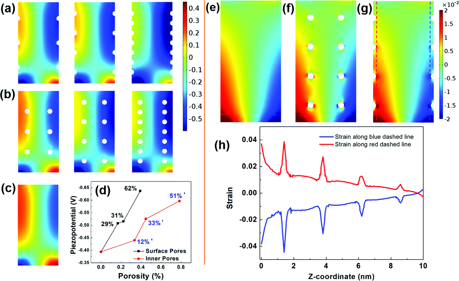 | ||
| Fig. 2 Piezopotential distribution in porous NWs with varying porosity under lateral bending force (10 nN) applied to the top surface of NWs, (a) with only surface pores, (b) with only inner pores, and (c) a non-porous NW. The scale bar in (a–c) is the same. (d) Comparison of negative piezopotential at the compressed side of NWs, as a function of porosity. Strain distribution in the yz-plane (at x = 0) for (e) the non-porous NW, (f) porous NW with only inner pores, and (g) porous NW with only surface pores. (h) Local strain profile along the dashed line of (g) in the c-direction across surface pores. | ||
In order to delve into this issue, both kinds of pores (2 nm in size) are combined and incorporated into a cylindrical shaped (10 nm radius and 150 nm height) c-plane ZnO NW. In the simulations, the total degree of porosity is fixed at 1.2%. We define the three models as a non-porous ZnO NW (N-ZnO), a porous ZnO NW with randomly distributed inner and surface pores (R-ZnO), and a porous ZnO NW with inner pores of random distribution and surface pores of density gradient distribution (GR-ZnO), as shown in Fig. 3 (Fig. S2, ESI†). For simplicity, surface pores in GR-ZnO are assumed to be only concentrated and equally distributed in the top half, leaving no surface pores in the bottom half, therefore, the gradient takes a simple form of step-like change. The two kinds of external forces are the same as before.
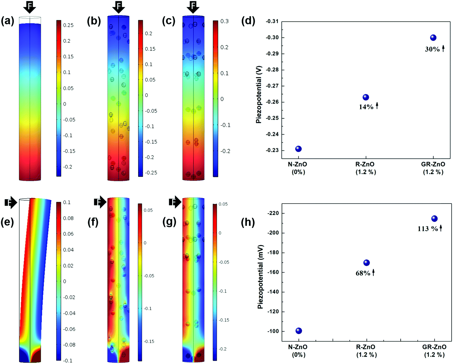 | ||
| Fig. 3 Piezopotential distribution under a normal compressive force (10 nN) applied to the top surface of NWs in (a) a non-porous ZnO NW (N-ZnO), (b) a porous ZnO NW with randomly distributed inner and surface pores (R-ZnO), and (c) a porous ZnO NW with inner pores of random distribution and surface pores of density gradient distribution (GR-ZnO). (d) Comparison of negative piezopotential at the +c polar surface. Piezopotential distribution under lateral bending force of 10 nN applied to the top surface of NWs in (e) N-ZnO, (f) R-ZnO, and (g) GR-ZnO. (h) Comparison of negative piezopotential at the compressed side of NWs. Deformations in NWs under normal compressive and bending forces are shown for N-ZnO. | ||
The simulation results in Fig. 3a–c clearly point out that the pore density distribution of the inner and surface pores has a profound effect on the relative magnitude of the piezopotential of the respective sides (+c and −c). The negative piezopotential at the +c polar surface is compared in Fig. 3d. The results reveal that the negative piezopotential is enhanced by 14% for the R-ZnO NW and by 30% for the GR-ZnO NW with respect to the N-ZnO NW. The simulation results in Fig. 1d and 3d suggest that the negative piezopotential at the top surface of a porous NW under compressive stress can be greatly boosted depending on the porosity and the spatial distribution of pores.
The reason for this significant enhancement of the negative piezopotential is that the generated piezopotential is strain-induced, and there is a localized high magnitude strain around each pore (Fig. 1f–h), which induces a higher piezopotential. When a normal compressive force is exerted on the top surface of the NW, the strain is negative (compressive strain) at the top side and positive (tensile strain) at the bottom side. At the same time, the high magnitude local strain around each pore is also positive and negative, as discussed above. Therefore, the spatial distribution of each pore will have an influence on the overall bulk strain. If the pore density is higher around the positive strain side of the NW, the negative piezopotential will be enhanced, and vice versa. In the present study (Fig. 3b, c and f, g), we have chosen the pore distribution to enhance the negative piezopotential to comply with the experimental results in this study; however, if the pore distribution is reversed, the positive piezopotential will be enhanced (Fig. S3, ESI†).
Fig. 3e–g show the simulation results for the bending case. Notably, the magnitude and the distribution of positive and negative piezopotentials are seriously affected by the presence and the distribution of pores inside a porous NW. Fig. 3h indicates that the negative piezopotential at the compressed side of the ZnO NW is increased by 68% for the R-ZnO NW and by 113% for the GR-ZnO NW, in comparison to the N-ZnO NW. Consequently, according to the simulation results in Fig. 2d and 3h, the piezopotential is more significantly improved in the bending case.
Therefore, the overall inference of this detailed simulation study of piezoelectric semiconductor NWs is that the piezopotential is certainly enhanced by the presence of pores, and its magnitude depends on the degree of porosity and the spatial distribution of the inner and surface pores.
To validate the above-mentioned simulation results, the piezoelectric semiconductor chosen in this work is ZnO, and ZnO NWs with different degrees of porosity are accomplished via hydrogen annealing for different durations of time (Fig. S4, S5 and Table S2, ESI†). Fig. 4a–c present scanning electron microscopy (SEM) images of the as-grown, 3 h, and 6 h hydrogen-annealed ZnO NW arrays, respectively.
 | ||
| Fig. 4 SEM images of the (a) as-grown, (b) 3 h, and (c) 6 h annealed ZnO NW arrays. (d) TEM images showing the pore-density gradient along the yellow arrow (bottom inset) and a diffraction pattern showing high crystallinity and wurtzite phase of the porous ZnO NWs (top left inset). (e–g) Current output mapping of piezoelectric DC-NGs from scanning a C-AFM tip with maximum output currents of (e) 1.18 nA for as-grown ZnO NWs (0HA-ZnO), (f) 8 nA for 3 h annealed (3HA-ZnO), and (g) 27.7 nA for 6 h annealed (6HA-ZnO) porous ZnO NWs. (h) Statistical data of output performance of the three types of nanogenerators. | ||
TEM images of the 3 h annealed porous ZnO NWs in Fig. 4d reveal the pore-density gradient (yellow arrowhead points to the bottom of the NW). The diffraction pattern in Fig. 4d demonstrates the wurtzite crystal structure with high crystallinity, even after being hydrogen-annealed. Inner pores are left behind upon decomposition and evaporation of residual precursors trapped inside the ZnO NWs after high temperature annealing.28,29 The surface pores are created by hydrogen etching.30 The distinction between these two types of pores can be identified by tilting the NWs in TEM (Fig. S6, ESI†).31
The microstructure of ZnO NWs has been modified by creating different degrees of porosity and the effect of porosity on DC piezoelectric NGs can be examined (Fig. S7, ESI†). Fig. 4e–g show the comparison of the output current of piezoelectric DC-NGs, by scanning the C-AFM Pt-coated tip across individual nanowires for the non-porous ZnO NWs (0HA-ZnO) and the porous ZnO NWs after annealing for 3 h (3HA-ZnO) and 6 h (6HA-ZnO), respectively.
Fig. 4e–g show striking results on tremendous enhancement of current output for ZnO NWs after incorporating pores. The statistical data on current output shown in Fig. 4h clearly demonstrate that the output current of ZnO NWs is significantly enhanced up to ∼23 times, from 1.18 nA of the as-grown ZnO NWs to 8 nA and 27.7 nA upon increasing the porosity to 2.6% and 5.4%, respectively, in the porous ZnO NWs. The surprising fact is that the validation results gave much higher values than the simulation results. Therefore, the underlying mechanisms responsible for this huge DC-NG performance enhancement are studied further.
The electrical conductivity of the three types of ZnO NWs (i.e., 0HA-ZnO, 3HA-ZnO, and 6HA-ZnO) is examined in Fig. S8a (ESI†), by measuring I–V curves with C-AFM, with minimal contact force (∼0.01 nN) to avoid the piezopotential effect. We found that the non-porous ZnO NW exhibits a rectifying behavior (red line, inset), while the porous ZnO NWs reveal double Schottky I–V characteristics. Apparently, porosity can significantly change the SBH with the same Pt electrode. Since hydrogen could act as a donor,32–34 thermionic field emission theory would be appropriate to dictate the I–V characteristics under reverse bias (positive applied voltage to the Pt–ZnO contact), where the tunneling current across the reverse SBH dominates.35,36 Under these circumstances, the thermionic field emission current density is expressed by eqn (S1) (ESI†).36–38 Consequently, for the as-grown non-porous ZnO NWs, carrier concentration Nd = 5.45 × 1017 cm−3 and effective SBH ϕb = 0.98 eV, whereas Nd increases to 7.97 × 1017 cm−3 and 9.50 × 1017 cm−3, and ϕb decreases to 0.75 eV and 0.73 eV, for porous ZnO NWs after annealing for 3 h and 6 h, respectively. Evidently, creating pores inside ZnO NWs enhances the free carrier concentration and thus, conductivity, accompanied by the corresponding reduction of SBH. Therefore, the pores not only increase the effective surface area, but presumably annealing in a hydrogen atmosphere can modify the surface states and cause a doping effect to enhance the conductivity, which is discussed in detail below.
Firstly, pores are under non-equilibrium conditions indicated by their irregular shape, revealed in Fig. S6c (ESI†), as opposed to the equilibrium hexagonal shape with low surface energy facets,30 and that facilitates the surface adsorption of hydrogen gas molecules. Hydrogen then desorbs the oxygen molecules that are generally adsorbed on the as-grown ZnO NW surface. This releases captured electrons back to the ZnO NWs and reduces the depletion regions, thereby increasing conductivity (Fig. S9, ESI†). Moreover, hydrogen is a well-known n-type shallow donor for ZnO. It can selectively attach to the dangling bond of the ZnO NW with both nonpolar and polar surfaces. It can also perforate into a lattice and defects in the form of interstitials (H+i),33,34,39 driving a doping process during surface pore creation and causing surface roughening by hydrogen etching. All these phenomena work synergistically to increase the free carrier concentration and to enhance the conductivity in porous ZnO NWs.
Therefore, the gigantic enhancement of the current output of porous ZnO NW based DC NGs can be attributed to three major mechanisms. The first one is the piezopotential enhancement due to the local strain around pores, as explored by comprehensive simulations. The hydrogen annealed porous ZnO NWs can be considered as GR-ZnO (Fig. 3) showing 118% enhancement of piezopotential, since the inner pores result from evaporation of trapped residual precursors that randomly distribute inside the NWs, while the surface pores are created by hydrogen etching following gradient diffusion from top to bottom. The second factor is the increased free carrier concentration and enhanced conductivity in porous NWs, which is below the optimum conductivity and thus, the reduction of inner resistance dominates over the carrier screening effect.40 The third one is the reduction in the relative permittivity of the porous nanostructure due to the introduction of low permittivity pores (which can be approximated with the permittivity of air). This further increases the piezopotential, but was not considered in the simulations. Finally, the effective piezoelectric coefficient (d33) of the porous NW is found to be higher than that of the non-porous NW (Fig. S10, S11 and Table S3, ESI†). This was also not considered in the simulation study.
We study the piezotronic effects of the three types of ZnO NWs (i.e., 0HA-ZnO, 3HA-ZnO, and 6HA-ZnO) through force-dependent I–V curves (Fig. 5). They are measured by a Pt-coated conductive tip with C-AFM (Fig. 5a–c), where normal forces of 0.01 (∼0), 1, 3 and 6 nano-newton (nN) are applied to single ZnO NWs. These axial forces act as a control for the gate electrode in traditional field effect transistors. Considering that hydrothermally synthesized ZnO NWs possess an upward pointing c-axis (i.e. Zn-terminated polar top surface) and the applied voltages are mostly consumed at the reverse Schottky contact, the compressive stress induces a negative piezopotential at the top Pt–ZnO contact. This suppresses the current non-linearly for all three types of ZnO NWs, as shown in Fig. 5a–c. Under an applied force of 6 nN at 1 V, the current drops by ∼97% (completely turns off) for the 6 h annealed porous ZnO NW (6HA-ZnO), and by ∼56% for the non-porous ZnO NW (0HA-ZnO), as shown in Fig. 5d. This suggests that both inner and surface pores in ZnO NW do enhance the negative piezopotential. This is in good agreement with the predictions from the simulation results in Fig. 1 and 3. This enhanced piezopotential can effectively turn on/off the current through a single NW based piezotronic device, acting as ideal SGTs.
 | ||
| Fig. 5 Force-dependent I–V characteristics as piezotronic properties of the three types of ZnO NWs, (a) as-grown ZnO NWs (0HA-ZnO), (b) 3 h annealed (3HA-ZnO), and (c) 6 h annealed (6HA-ZnO) porous ZnO NWs, examined by C-AFM using normal forces of 0.01, 1, 3 and 6 nN. (d) Corresponding current drops as a function of applied force at 1.0 V. (e) Calculated change of SBH as a function of applied force at 1.0 V, where the lines correspond to the linear fitting function and their slopes determine the force sensitivity of the SGT devices. | ||
Moreover, the corresponding change of SBH, related to the piezopotential in controlling carrier transport across interfaces of piezotronics, can be derived from eqn (S5) (ESI†).41Fig. 5e reveals a positive correlation between the change of SBH and pore density. Under an applied normal force of 6 nN, the change of SBH at the Pt–ZnO interface equals 0.025 eV for the as-grown 0HA-ZnO NW, 0.06 eV for the 3HA-ZnO NW, and 0.08 eV for the 6HA-ZnO NW. These results indicate that the piezopotential of a piezoelectric semiconductor can be boosted simply by creating pores, and it exhibits an increasing trend with porosity. This is also in good agreement with the simulation results in Fig. 1–3. Furthermore, the slope of SBH change on applied force (Fig. 5e) is regarded as ‘force sensitivity’, which is improved from 2.27 ± 0.44 meV nN−1 for the non-porous ZnO NWs to 8.07 ± 1.65 and 14.24 ± 0.89 meV nN−1 for the 3 h and 6 h porous ZnO NWs, respectively. This indicates that the porosity is critical and more versatile for tuning force sensitivity, which can be extensively improved by ∼6 times (∼527% increment), implying that pores can augment the performance of piezotronic devices significantly.
Conclusions
In summary, we have revealed through simulation studies that altering the microstructure using discontinuous inner and surface nano-pores in one-dimensional nanostructures of piezoelectric semiconductors can substantially enhance the piezopotential, and the piezopotential distribution depends on the degree of porosity and the spatial distribution of pores inside the nanostructures. The theoretical finding is also verified experimentally, by the fabrication of devices based on porous nanowires, using ZnO as a model piezoelectric semiconductor. The porous ZnO NWs can be easily synthesized via a hydrothermal method followed by hydrogen annealing. A NG device based on porous ZnO NW arrays can generate DC electricity ∼23 times higher than that based on the as-grown NW arrays. This striking result is ascribed to the pore-induced piezopotential enhancement, as well as free carrier concentration and conductivity enhancement with porosity, along with permittivity reduction. Surface state modification revealed by randomly shaped pores in the porous ZnO NWs, oxygen molecule desorption, and hydrogen as an n-type shallow donor are the three contributing factors to conductivity enhancement. Pore-induced piezopotential enhancement has also been demonstrated in piezotronics, via force-dependent I–V curves in strain-gated transistors (SGTs), which can effectively turn on/off the current through a single NW based piezotronic device, acting as ideal SGTs. Moreover, the slope of SBH change, as ‘force sensitivity’, demonstrates ∼6 times (∼527% increment) enhancement in the porous NW based SGT device.In practice, porous nanostructures incorporated into piezotronics devices can be highly beneficial for many current applications. Due to the conductivity improvement and pore induced piezopotential enhancement inside the piezoelectric semiconductor NW, the performance of piezoelectric DC-NGs and piezotronics (such as various sensors and transistors) can be considerably improved by applying this strategy.
Experimental section
Simulations
The simulation study was conducted to calculate the dependence of porosity on piezopotential using the finite-element analysis software, COMSOL Multiphysics 5.1. The material properties of ZnO are given in Table S1 (ESI†).Synthesis
The scheme of materials preparation is shown in Fig. S4 (ESI†). Arrays of ZnO NWs were first grown on a Si(100) substrate covered with a sputtered ZnO seed layer by hydrothermal synthesis using a solution of hexamethylenetetramine and zinc acetate (ratio 1![[thin space (1/6-em)]](https://www.rsc.org/images/entities/char_2009.gif) :1) for 9 h. The samples were then baked dry on a hot plate for 15 minutes at 80 °C. Finally, the porous nanostructures in ZnO NWs were formed by hydrogen annealing (Ar(g):H2(g) = 80:20) in a tube furnace at 500 °C for 0 h (0HA), 3 h (3HA) and 6 h (6HA). The porous NWs started to collapse upon prolonged annealing for 9 h. The morphology of the as-grown and porous ZnO NW arrays is shown in Fig. 4 and in Fig. S5 and S6 (ESI†), with the porosity calculated in Table S2 (ESI†).
:1) for 9 h. The samples were then baked dry on a hot plate for 15 minutes at 80 °C. Finally, the porous nanostructures in ZnO NWs were formed by hydrogen annealing (Ar(g):H2(g) = 80:20) in a tube furnace at 500 °C for 0 h (0HA), 3 h (3HA) and 6 h (6HA). The porous NWs started to collapse upon prolonged annealing for 9 h. The morphology of the as-grown and porous ZnO NW arrays is shown in Fig. 4 and in Fig. S5 and S6 (ESI†), with the porosity calculated in Table S2 (ESI†).
Characterization
Surface and cross-sectional morphology was analyzed by field-emission scanning electron microscopy (SEM, HITACHI SU8000) using secondary electron imaging operated at 5 kV. Transmission electron microscopy (TEM, Cs-corrected JEOL 2100F) was used to investigate the microstructure of nano-pores and confirm the phase of ZnO NWs.Piezotronic measurement
Current output mapping and stress dependent current–voltage (I–V) characteristics of the as-grown and the porous ZnO NWs were performed by conductive atomic force microscopy (C-AFM), using a Pt-coated tip as the top electrode and silver paste as the bottom electrode, as illustrated in Fig. S7 (ESI†).Conflicts of interest
There are no conflicts to declare.Acknowledgements
We acknowledge financial support from the Ministry of Science and Technology of Taiwan under grants MOST 107-2221-E-006-020-MY3 and MOST 107-3017-F-006-003. The authors wish to thank the Center for Micro/Nano Science and Technology, National Cheng Kung University, for providing equipment and technical support. This work was also financially supported by the Hierarchical Green-Energy Materials (Hi-GEM) Research Center, from The Featured Areas Research Center Program within the framework of the Higher Education Sprout Project by the Ministry of Education (MOE) in Taiwan. The authors wish to thank Prof. Chen Yi-Chun of the Department of Physics, National Cheng Kung University, for help with the piezoelectric coefficient measurements by using PFM.References
- R. Yu, X. Wang, W. Peng, W. Wu, Y. Ding, S. Li and Z. L. Wang, ACS Nano, 2015, 9, 9822–9829 CrossRef CAS PubMed.
- Z. L. Wang and J. Song, Science, 2006, 312, 242–246 CrossRef CAS PubMed.
- C. Soci, A. Zhang, B. Xiang, S. A. Dayeh, D. Aplin, J. Park, X. Bao, Y.-H. Lo and D. Wang, Nano Lett., 2007, 7, 1003–1009 CrossRef CAS PubMed.
- X. Cao, X. Cao, H. Guo, T. Li, Y. Jie, N. Wang and Z. L. Wang, ACS Nano, 2016, 10, 8038–8044 CrossRef CAS PubMed.
- H. Li, N. Liu, X. Zhang, J. Su, L. Li, Y. Gao and Z. L. Wang, Nano Energy, 2016, 27, 587–594 CrossRef CAS.
- W. Chao-Hung, L. Wei-Shun, L. Zong-Hong, K. Nai-Jen, L. Yi-Chang, C. Yen-Chih, W. Zhong-Lin and L. Chuan-Pu, Adv. Energy Mater., 2014, 4, 1400392 CrossRef.
- D.-M. Shin, H. J. Han, W.-G. Kim, E. Kim, C. Kim, S. W. Hong, H. K. Kim, J.-W. Oh and Y.-H. Hwang, Energy Environ. Sci., 2015, 8, 3198–3203 RSC.
- J. Briscoe, N. Jalali, P. Woolliams, M. Stewart, P. M. Weaver, M. Cain and S. Dunn, Energy Environ. Sci., 2013, 6, 3035–3045 RSC.
- W. Zeng, X.-M. Tao, S. Chen, S. Shang, H. L. W. Chan and S. H. Choy, Energy Environ. Sci., 2013, 6, 2631–2638 RSC.
- Q. Zhong, J. Zhong, B. Hu, Q. Hu, J. Zhou and Z. L. Wang, Energy Environ. Sci., 2013, 6, 1779–1784 RSC.
- L. Lin, Q. Jing, Y. Zhang, Y. Hu, S. Wang, Y. Bando, R. P. S. Han and Z. L. Wang, Energy Environ. Sci., 2013, 6, 1164–1169 RSC.
- J.-H. Lee, K. Y. Lee, B. Kumar, N. T. Tien, N.-E. Lee and S.-W. Kim, Energy Environ. Sci., 2013, 6, 169–175 RSC.
- M. Lee, J. Bae, J. Lee, C.-S. Lee, S. Hong and Z. L. Wang, Energy Environ. Sci., 2011, 4, 3359–3363 RSC.
- J. Kwon, W. Seung, B. K. Sharma, S.-W. Kim and J.-H. Ahn, Energy Environ. Sci., 2012, 5, 8970–8975 RSC.
- V. F. Rivera, F. Auras, P. Motto, S. Stassi, G. Canavese, E. Celasco, T. Bein, B. Onida and V. Cauda, Chem. – Eur. J., 2013, 19, 14665–14674 CrossRef CAS PubMed.
- M. Riaz, J. Song, O. Nur, Z. L. Wang and M. Willander, Adv. Funct. Mater., 2011, 21, 628–633 CrossRef CAS.
- A. Khan, M. Hussain, O. Nur and M. Willander, J. Phys. D: Appl. Phys., 2014, 47, 345102 CrossRef.
- Y.-T. Chang, J.-Y. Chen, T.-P. Yang, C.-W. Huang, C.-H. Chiu, P.-H. Yeh and W.-W. Wu, Nano Energy, 2014, 8, 291–296 CrossRef CAS.
- J. I. Sohn, S. N. Cha, B. G. Song, S. Lee, S. M. Kim, J. Ku, H. J. Kim, Y. J. Park, B. L. Choi and Z. L. Wang, Energy Environ. Sci., 2013, 6, 97–104 RSC.
- S.-H. Shin, Y.-H. Kim, M. H. Lee, J.-Y. Jung, J. H. Seol and J. Nah, ACS Nano, 2014, 8, 10844–10850 CrossRef CAS PubMed.
- C. Liu, M. Peng, A. Yu, J. Liu, M. Song, Y. Zhang and J. Zhai, Nano Energy, 2016, 26, 417–424 CrossRef CAS.
- Y. Zhang, C. Liu, J. Liu, J. Xiong, J. Liu, K. Zhang, Y. Liu, M. Peng, A. Yu and A. Zhang, ACS Appl. Mater. Interfaces, 2016, 8, 1381–1387 CrossRef CAS PubMed.
- T. T. Pham, K. Y. Lee, J.-H. Lee, K.-H. Kim, K.-S. Shin, M. K. Gupta, B. Kumar and S.-W. Kim, Energy Environ. Sci., 2013, 6, 841–846 RSC.
- J. I. Sohn, S. N. Cha, B. G. Song, S. Lee, S. M. Kim, J. Ku, H. J. Kim, Y. J. Park, B. L. Choi, Z. L. Wang, J. M. Kim and K. Kim, Energy Environ. Sci., 2013, 6, 97–104 RSC.
- N. J. Ku, C. H. Wang, J. H. Huang, H. C. Fang, P. C. Huang and C. P. Liu, Adv. Mater., 2013, 25, 861–866 CrossRef CAS PubMed.
- C.-Y. Chen, J.-H. Huang, J. Song, Y. Zhou, L. Lin, P.-C. Huang, Y. Zhang, C.-P. Liu, J.-H. He and Z. L. Wang, ACS Nano, 2011, 5, 6707–6713 CrossRef CAS PubMed.
- H. Li, X. Zhang, N. Liu, L. Ding, J. Tao, S. Wang, J. Su, L. Li and Y. Gao, Opt. Express, 2015, 23, 21204–21212 CrossRef CAS PubMed.
- K. G. Yu-Lun Su, R.-C. Wang and C.-P. Liu, unpublished results.
- S. H. Lee, H. J. Lee, H. Goto, M. W. Cho and T. Yao, Phys. Status Solidi C, 2007, 4, 1747–1750 CrossRef CAS.
- J. Ghatak, J.-H. Huang, P.-C. Huang, Y.-I. Shih and C.-P. Liu, J. Electrochem. Soc., 2012, 159, H239–H242 CrossRef CAS.
- K. Gupta, J.-T. Lin, R.-C. Wang and C.-P. Liu, NPG Asia Mater., 2016, 8, e314 CrossRef CAS.
- A. Janotti and C. G. Van de Walle, Rep. Prog. Phys., 2009, 72, 126501 CrossRef.
- S. Koch, E. Lavrov and J. Weber, Phys. Rev. B: Condens. Matter Mater. Phys., 2014, 90, 205212 CrossRef.
- H. F. Wilson and A. S. Barnard, J. Phys. Chem. C, 2015, 119, 26560–26565 CrossRef CAS.
- Y. Liu, Y. Zhang, Q. Yang, S. Niu and Z. L. Wang, Nano Energy, 2015, 14, 257–275 CrossRef CAS.
- Z. Zhang, K. Yao, Y. Liu, C. Jin, X. Liang, Q. Chen and L. M. Peng, Adv. Funct. Mater., 2007, 17, 2478–2489 CrossRef CAS.
- E. Rhoderick, R. Williams and M.-S. Contacts, Metal-Semiconductor Contacts, Oxford, 1988 Search PubMed.
- R. Yu, L. Dong, C. Pan, S. Niu, H. Liu, W. Liu, S. Chua, D. Chi and Z. L. Wang, Adv. Mater., 2012, 24, 3532–3537 CrossRef CAS PubMed.
- S. J. Baik, J. H. Jang, C. H. Lee, W. Y. Cho and K. S. Lim, Appl. Phys. Lett., 1997, 70, 3516–3518 CrossRef CAS.
- C. H. Wang, W. S. Liao, N. J. Ku, Y. C. Li, Y. C. Chen, L. W. Tu and C. P. Liu, Small, 2014, 10, 4718–4725 CrossRef CAS PubMed.
- J. Zhou, Y. Gu, P. Fei, W. Mai, Y. Gao, R. Yang, G. Bao and Z. L. Wang, Nano Lett., 2008, 8, 3035–3040 CrossRef CAS PubMed.
Footnotes |
| † Electronic supplementary information (ESI) available. See DOI: 10.1039/c8ee02081g |
| ‡ These authors contributed equally. |
| This journal is © The Royal Society of Chemistry 2019 |