
Challenges and prospects of 3D micro-supercapacitors for powering the internet of things
Christophe
Lethien
 *ab,
Jean
Le Bideau
bc and
Thierry
Brousse
bc
*ab,
Jean
Le Bideau
bc and
Thierry
Brousse
bc
aInstitut d'Electronique, de Microélectronique et de Nanotechnologies (IEMN), Université de Lille, CNRS, Centrale Lille, ISEN, Univ. Valenciennes, F-59000 Lille, France. E-mail: christophe.lethien@univ-lille.fr
bRéseau sur le Stockage Electrochimique de l’Energie, CNRS FR 3459, 33 rue Saint Leu, 80039 Amiens Cedex, France
cInstitut des Matériaux Jean Rouxel, CNRS UMR 6502 – Université de Nantes, 2 rue de la Houssinière BP32229, 44322 Nantes cedex 3, France
First published on 9th October 2018
Abstract
The fabrication of miniaturized electrochemical energy storage systems is essential for the development of future electronic devices for Internet of Things applications where connected devices are increasingly deployed in our daily life. On chip micro-supercapacitors are an attractive solution to fulfill the energy requirements of autonomous, smart, maintenance free and miniaturized sensors but they suffer from a limited energy density and poor technological readiness level in spite of high power capabilities and long cycle life. This paper aims at reviewing the current micro-supercapacitor technologies and at defining the guidelines to produce high performance micro-devices with special focus on 3D designs as well as the fabrication of solid state miniaturized devices to solve the packaging issue.
 Christophe Lethien | Christophe Lethien is an Associate Professor from University of Lille. He works at Institute of Electronics, Microelectronics and Nanotechnologies (IEMN, CNRS UMR 8520) and in the framework of the French network on electrochemical energy storage (RS2E, CNRS FR 3459). He received his PhD from University of Lille in 2004. From 2004 to 2007, he got a research scientist position at Royal Military Academy from Brussels (Belgium) in the field of photonics and sensor networks. Since 2008, his research focuses on developing emerging technologies on electrochemical storage miniaturized devices that address the Internet of Things challenge. In particular, he is strongly involved in the collective fabrication of Li-ion micro-batteries and micro-supercapacitors based on thin film technologies. |
 Jean Le Bideau | Jean Le Bideau is Professor at University of Nantes, Institut des Matériaux Jean Rouxel (IMN, CNRS UMR 6502), since 2008, after ten years at University of Montpellier as Associate Professor, and two years at Michigan State University as Associate Researcher. His researches aim at confining soft matter within host networks, either as hydrogels for biomedical purposes, or as ionogels for energy storage. In the case of energy storage, ionogels allow to obtained all-solid devices endowed with the properties of ionic liquids. Focus is made on interfacial and confinement effects, in order to gain understanding on the origin of the good dynamics and diffusion properties of the confined species. |
 Thierry Brousse | Thierry Brousse is a Professor of Materials Science. He received his PhD degree in 1991. After being a chemical engineer in a company, he joined the University of Nantes in 1994 where he occupies a Full Professor position since 2005. He is a researcher at Institut des Matériaux Jean Rouxel (IMN) and works within the framework of the French network on electrochemical energy storage (RS2E). His research focuses on materials for electrochemical energy storage with particular emphasis on innovative and/or modified materials for electrochemical capacitors and related devices. He is vice-dean of the University of Nantes in charge innovation since 2013. |
Broader contextThe development of high energy density and solid state micro-supercapacitors is one of the greatest technological challenges at the dawn of the Internet of Things. Smart and miniaturized power sources are key technologies for the development of cutting edge wireless sensor networks for transportation, health and industrial monitoring as well as for environmental applications. The combination of electrochemical capacitors with energy harvesting/ scavenging devices is essential for the fabrication of autonomous sensor nodes. This proposal is meaningful at the millimeter scale for miniaturized sensors. The high power capabilities and long cycle life of micro-supercapacitors are attractive properties to solve the autonomy issue but the energy density has to be significantly improved while the packaging and safety issues have to be solved. This article reports on a critical review of up-to-date micro-supercapacitor technologies and describes the main challenges and prospects to improve the overall performance and the technological readiness level. |
1. Introduction – scope of the review
The internet of things (IoT) is a trendy concept used to describe the exchange of data between portable, smart and connected devices.1,2 Such electronic devices could be used as sensors or could be controlled remotely across existing network structures, thus creating opportunities for bridging hardware and software applications in order to design efficient, accurate, self-powered and maintenance-free systems with limited human intervention. Energy scavenging/harvesting technologies are widely investigated for IoT devices to produce self-powering systems with harvesting from thermal, mechanical or solar energy from the environment and conversion into electricity. Unfortunately, the intermittence and instability of such resources impose the use of energy storage technologies compatible with the desired application. Miniaturized sensor nodes are required within IoT networks for health, environmental or industrial monitoring, drug delivery (in vivo application), transportation, wearable personal electronics, and radio frequency identification systems. However, it is still challenging to drive these small and connected devices from an energy point of view. The miniaturization of different types of electrochemical energy storage (EES) technologies has been widely investigated for several years in order to produce efficient EES devices. Li-ion micro-batteries3–5 (MB) and micro-supercapacitors6–12 (MSC) are two complementary EES miniaturized systems and have to be used in the energy storage unit of IoT devices. While MB offer high energy (1 mW h cm−2) and moderate power densities (<5 mW cm−2), MSC are particularly attractive for high power applications (>10 mW cm−2) but suffer from a lack of energy density (<0.1 mW h cm−2). The charge storage processes occurring in MB and MSC are totally different in nature leading to complementary properties. MSC based on capacitive ion adsorption/desorption in carbon porous electrodes10,13,14 offer optimum cycle life (>1![[thin space (1/6-em)]](https://www.rsc.org/images/entities/char_2009.gif) 000000 cycles) and high power density: such miniaturized EES devices are characterized by rectangular shape cyclic voltammograms and linear galvanostatic charge–discharge profiles. Similar features are observed with MSC based on pseudocapacitive materials8,9,15 where fast redox surface reactions are responsible for the continuous change of oxidation state of the cations in the electrode material:16,17 no phase change is observed in pseudocapacitive materials during cycling and the electrochemical signatures are capacitive-like. Redox reactions taking place in MB are similar to those occurring in large scale Li-ion batteries.
000000 cycles) and high power density: such miniaturized EES devices are characterized by rectangular shape cyclic voltammograms and linear galvanostatic charge–discharge profiles. Similar features are observed with MSC based on pseudocapacitive materials8,9,15 where fast redox surface reactions are responsible for the continuous change of oxidation state of the cations in the electrode material:16,17 no phase change is observed in pseudocapacitive materials during cycling and the electrochemical signatures are capacitive-like. Redox reactions taking place in MB are similar to those occurring in large scale Li-ion batteries.
The current review aims at focusing on micro-supercapacitor technology. In particular, we discuss about the recent progress and challenges to produce high energy density solid state MSC compatible with microelectronic facilities. The first part of this review is dedicated to the description of the topologies and the adequate metrics used to report the general performance of MSC. This part is concluded with a description of electrode materials suitable for MSC. Then, the reported strategies to produce MSC based on thin or thick film technologies are discussed. As the energy density is thickness-limited, a large part of this review is focused on MSC based on 3D architectures taking into account the fabrication of high specific area MSC with high mass loading and robust 3D scaffolds. Finally, this review focuses on the electrolyte and packaging issues for MSC which are considered as one of the main technological barriers to improve the technological readiness level (TRL) of such miniaturized EES devices.
2. Topologies and performance metrics for micro-supercapacitors
The charge storage process involved in supercapacitors and micro-supercapacitors is similar. It is based on capacitive ion adsorption/desorption in porous or nanometer size carbon. Alternatively, pseudocapacitive materials store charge via fast and reversible redox reactions providing a capacitive-like electrochemical signature. The energy and power densities reached by a MSC are not only dependent on the material properties but also on the topology or configuration of the device. A supercapacitor is composed of two current collectors, two porous electrodes and a separator soaked with a liquid electrolyte. Micro-supercapacitors are considered as a class of miniaturized supercapacitors having a footprint close to several square millimeters. During the last decade, micro-supercapacitors exhibiting high energy and power performance have been reported but the metrics used to normalize the performance are not suitable for miniaturized EES despite the publication of several recent papers focusing on this topic18–20 and defining the guidelines to report the performance of miniaturized EES devices. The performance of supercapacitors is generally reported using gravimetric values of the capacitance, the power and the energy of the devices (F g−1, W kg−1, W h kg−1). Unfortunately, small size MSC are surface dependent devices and the metrics used to compare the energy and power performance should be tailored to microsystem applications where gravimetric values are useless. In this review, capacitance, energy and power densities are reported respectively in mF cm−2, μW h cm−2 and mW cm−2, leading to footprint areal or surface properties which are the main issue when the surface is limited as in smart and connected miniaturized sensors. At this stage it must be noted that capacitance values are only valid whenever a capacitive-like behavior is shown for an electrode or a device. Unfortunately many confusing papers are now reporting so called pseudocapacitive behavior of nickel or cobalt based oxides or hydroxides in the literature which is wrong and misleading. A recent paper describes the difference between these different kinds of behavior,17 and a perspective paper indicates how to use the different metrics.20 Obviously when a battery-type electrode or device is proposed, only capacity values can be provided (in C g−1, mC cm−2, mA h g−1, or mA h cm−2).Volumetric normalized performance (per cm3) is also widely reported for MSC. While this metric is more suitable for miniaturized EES devices than gravimetric normalization, some misunderstanding or overstatement of the performance is reported for very thin film electrodes (nanometer-thick) and the outstanding volumetric value significantly decreases when the thickness of the active material is increased – if the deposition technique allows one to deposit a thicker layer. In order to clearly compare the performance of MSC, the surface metrics could be normalized to the thickness of the active layer giving rise to mF cm−2 μm−1, mC cm−2 μm−1, μW h cm−2 μm−1 and mW cm−2 μm−1. Such metrics are widely reported in the field of micro-batteries and could be easily transferred to MSC. In a micro-supercapacitor, the amount of active material (current collectors, electrodes and electrolyte) could be meaningless as compared to the amount of non-active material (substrate, packaging). While this strong argument is pertinent when thin film technology (thickness of the electrode <5 μm vs. thickness of substrate ∼500 μm) compatible with the microelectronics industry is used for the fabrication of MSC, most of the reported MSC are based on thick film technology where the electrodes could be thicker than 200 μm. In that case, the amounts of active vs. inactive materials are within the same order of magnitude.
Taking into account surface or areal normalized capacitance, the configuration of the MSC severely impacts the performance (Fig. 1). As a matter of fact, the parallel plate configuration (Fig. 1B) is the most efficient topology when the footprint is limited. The cell areal capacitance (CMSC) is half of the surface capacitance of the single electrode if a symmetric device is considered (CMSC = Celectrode/2) (Fig. 1A).
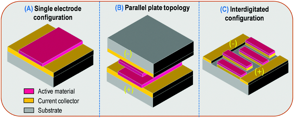 | ||
| Fig. 1 Overview of the topologies used in the field of micro-supercapacitors. | ||
Although this configuration is very attractive from a surface point of view, the total volume of the MSC is double since two substrates have to be used to support the two electrode deposition on current collectors. In between the two plates, a liquid or gel-like electrolyte is used to achieve the MSC fabrication. Due to the thickness of the substrate this stacked design leads to a huge volume which is usually not compatible with MSC applications.
Therefore, as no performing ceramic electrolyte with high ionic conductivity at room temperature is available, only liquid or gel-like electrolytes have to be used. Consequently, the stacked configuration is unusable from a technological point of view as it is impossible to deposit an electrode on a liquid or gel-like electrolyte, especially if the vacuum deposition technique is used for the electrode preparation. Hence, to reduce the compactness of the MSC while keeping the same footprint area, the two electrodes should be placed in the same plane, i.e. on the same substrate. Interdigitated or interdigital topology is the most suitable configuration for MSC applications. However, the active material per electrode is reduced (pink color – Fig. 1C) taking into account a reduction by a factor 2 of the active area per electrode and the inactive gap between the two interdigitated electrodes. Consequently, the cell surface capacitance in such topology is less than one fourth of the areal capacitance of a single electrode (CMSC < Celectrode/4). Considering the inactive gap between the two interdigitated electrodes is minimized as compared to the total areal of the MSC, we further consider in this review that CMSC = Celectrode/4, in order to compare the performance of MSC (see Tables 1–3). It has nevertheless to be pointed out that the inactive gap is advantageously exploited since it defines the electrolyte localization and thus its thickness. Different shapes of the interdigitated electrodes are reported. While the classical pattern (Fig. 1C) is used in 99% of the reported publications, recent work on spiral-shaped designed interdigitated electrodes for micro-supercapacitors was reported to improve the energy and power densities.21
| Ref. | Electrode materiala | Electrode capacitance* | Areal power density | Device topology | Electrolyteb/cell voltage (V) | |
|---|---|---|---|---|---|---|
| Deposition technique | Thickness (μm) | (mF cm−2) | (mW cm−2) | |||
| a AC = activated carbon, rGO = reduced graphene oxide, MWCNT = multiwall carbon nanotubes, CDC = carbide derived carbon, PPy = polypyrrole, LbL = layer by layer, ED = electrodeposition, IJP = inkjet printing, * if not mentioned, estimated from Celectrode = 4 × CMSC for the interdigitated topology and Celectrode = 2 × CMSC for the parallel plate configuration. b EMIM = 1-ethyl-3-methylimidazolium, TFSI = bis(trifluoromethanesulfonyl)imide, NEt4 = tetraethylammonium, BF4 = tetrafluoroborate, PEGDA = poly(ethylene glycol)diacrylate, PVA = poly(vinyl alcohol), PC = propylene carbonate, AN = acetonitrile, i = max of the instantaneous power, ii = maximum power. | ||||||
| 159 | Ppy (ED) | 2.5 | — | — | Interdigitated | 0.1 M H3PO4 |
| 38 | Graphene (plasma rGO) | 0.015 | 0.32 | 0.75i | Interdigitated | PVA H2SO4/1 V |
| 73 | MWCNT (LbL) | 0.25 | 0.32 | 0.8i | Interdigitated | Ionogel (EMIM–TFSI/PEGDA)/3 V |
| 72 | MWCNT/Mn3O4 (LbL) | 0.22 | 0.64 | 0.5i | Interdigitated | PVA H3PO4/0.8 V |
| 74 | MWCNT (spray coating) | 0.5 | 1.04 | 1.05i | Interdigitated | Ionogel (EMIM–TFSI/PEGDA)/2 V |
| 160 | MnO2–Au stacked layers (e-beam evaporation) | 0.05 | 1.6 | 0.017i | Interdigitated | PVA H2SO4/0.8 V |
| 161 | RuO2 (sputtering) | 0.2 | 2.8 | — | Parallel plate | LIPON/2.5 V |
| 162 | rGO (solution) | 1.2 | 3.2 | 0.09i | Interdigitated | PVA KOH/0.8 V |
| 163 | TiC–CDC (sputtering) | 1.6 | 6 | 84ii | Interdigitated | 1 M NEt4–BF4 in PC |
| 164 | AC (IJP) | 2 | 8.4 | 44.9ii | Interdigitated | 1 M NEt4–BF4 in PC/2.5 V |
| 32 | MWCNT (IJP) and MnO2 (ED) | 0.5 and 0.6 | 9.6 | 675ii | Interdigitated | 0.5 M Na2SO4/1.8 V |
| 11 | Mxene Ti3C2 (spray coating) | 1.3 | 27 | 1.95i | Interdigitated | PVA H2SO4/0.6 V |
| 65 | RuO2 (sputtering) | 0.3 | 45.6 | — | Parallel plate | LIPON/2 V |
| 75 | MnO2–Au stacked layers (ED and sputtering) | 1.6 | 48 | — | Interdigitated | 1 M Na2SO4/0.8 V |
| 13 | TiC–CDC (sputtering) | 4.1 | 69 | 100i | Parallel plate | 2 M EMIM–BF4 in AN/3 V |
| 57 | W-RuO2 (sputtering) | 1 | 100 | — | Parallel plate | LIPON/2 V |
| 7 | TiC–CDC (sputtering) | 3.2 | 103 | 100i | Single electrode | 1 M H2SO4/0.9 V |
| 13 | TiC–CDC (sputtering) | 5 | 205 | — | Interdigitated | 1 M H2SO4/0.9 V |
| 58 | VN (sputtering) | 3.4 | 220 | 10i | Interdigitated | 1 M KOH/0.6 V |
| Ref. | Electrode materiala | Electrode capacitance* | Areal power density | Device topology | Electrolyteb/cell voltage (V) | |
|---|---|---|---|---|---|---|
| Deposition technique | Thickness (μm) | (mF cm−2) | (mW cm−2) | |||
| a LSG = laser-scribed graphene, CVD = chemical vapour deposition, ESD = electrostatic spray deposition, DLW = direct laser writing, BDP = bundle drawing procedure, OLC = onion like carbon, EPD = electrophoretic deposition, ED = electrodeposition, IDP = injecting drying process, LIG = laser induced graphene, AC = activated carbon, rGO = reduced graphene oxide, CNT = carbon nanotubes, VA CNT = vertically aligned CNT, CDC = carbide derived carbon, PANI = polyaniline, G–VNQD = graphene and vanadium nitride quantum dots, * if not mentioned, estimated from Celectrode = 4 × CMSC for the interdigitated topology and Celectrode = 2 × CMSC for the parallel plate configuration. b BMIM = 1-butyl-3-methylimidazolium, EMIM = 1-ethyl-3-methylimidazolium, TFSI = bis(trifluoromethanesulfonyl)imide, NEt4 = tetraethylammonium, BF4 = tetrafluoroborate, PIP13 = N-methyl-N-propylpiperidinium, FSI = bis(fluorosulfonyl)imide, PYR14 = N-butyl-N-methylpyrrolidinium, PEGDA = poly(ethylene glycol)diacrylate, PVA = poly(vinyl alcohol), TMOS = tetramethyl orthosilicate, PC = propylene carbonate, ACN = acetonitrile, i = max of the instantaneous power, ii = maximum power. | ||||||
| 165 | VA CNT (CVD) | 50 | 1.2 | 100i | Interdigitated | Ionogel (EMIM–TFSI/TMOS)/3 V |
| 35 | rGO electrode (GO filtration and DLW) | 22 | 2 | 220i | Parallel plate | 1 M Na2SO4/1 V |
| 166 | OLC (EPD) | 7 | 4.4 | 240ii | Interdigitated | PIP13–FSI–PYR14–FSI ionic liquid/3.7 V |
| 85 | rGO–CNT electrode (ESD) | 6 | 5 | 46.2i | Interdigitated | 3 M KCl/1 V |
| 31 | OLC (EPD) | 7 | 6.8 | 210i | Interdigitated | 1 M NEt4–BF4 in PC/3 V |
| 14 | Graphene (LSG) | 7.6 | 7.1 | 152i | Interdigitated | Ionogel (BMIM–TFSI/fused silica)/2.5 V |
| 167 | Graphene–CNT electrode (CVD) | 20 | 8 | 60i–230ii | Interdigitated | 1 M Na2SO4/1 V |
| 14 | Graphene (LSG) | 7.6 | 9.1 | 53i | Interdigitated | PVA H2SO4/1 V |
| 31 | AC (EPD) | 5 | 18 | 20i | Interdigitated | 1 M NEt4–BF4 in PC/3 V |
| 168 | rGO–Au composite electrode (solution and DLW) | 13.7 | 20 | — | Interdigitated | PVA H2SO4/1 V |
| 169 | TiC–CDC (sputtering) | 7 | 72 | 5.3i | Single electrode | 2 M EMIM–BF4 in ACN/3 V |
| 170 | Graphene–FeOOH/graphene–MnO2 electrodes (LIG combined with ED) | 41 | 88 | 11.8i | Interdigitated | PVA LiCL/1.8 V |
| 171 | Vertically aligned Nb nanowires (BDP) | 1000 | 100 | 1000i | Parallel plate | 1 M H2SO4/1 V |
| 172 | AC and MnO2 (IDP) | 10 | 120 | 7i | Interdigitated | 0.2 M K2SO4/1.5 V |
| 98 | Graphene/RuO2 (LSG) | 7.6 | 160 | 6i | Interdigitated | 1 M H2SO4/1 V |
| 173 | PANI nanowires (ED) | 10.1 | 180 | 10.1i | — | PVA H2SO4/0.9 V |
| 80 | AC (screen printing) | 215 | 324 | 34.4i | Interdigitated | 1 M NEt4–BF4 in PC/2.5 V |
| 174 | Graphene–PANI staked electrode (LbL) | 4.5 | 326 | 4.5i | Interdigitated | PVA H2SO4/1 V |
| 175 | AC (solution injection) | 70 | 360 | 51.5i | Interdigitated | 1 M NaNO3/1 V |
| 77 | AC (solution injection) | 250 | 536 | 4.5i | Interdigitated | PVA H3PO4/1 V |
| 78 | AC (solution injection) | 100 | 640 | 31.2i | Interdigitated | BMIM–BF4 ionic liquid |
| 81 | V2O5 and G–VNQD electrodes (3D printing) | 100 | 832 | 3.77i | Interdigitated | PVA LiCL/1.6 V |
| 79 | AC (solution injection) | 200 | 1244 | 10i | Interdigitated | BMIM–BF4 ionic liquid/3 V |
| Ref. | Electrode configuration | Electrode materiala | 3D scaffold | Electrode capacitance* (mF cm−2) | Areal power density (mW cm−2) | Device topology | Electrolyteb/cell voltage (V) | ||
|---|---|---|---|---|---|---|---|---|---|
| Deposition technique | Thickness (μm) | Materials/shape (fabrication technique) | Depth (μm) | ||||||
| a LSG = laser-scribed graphene, CVD = chemical vapour deposition, ED = electrodeposition, PANI = polyaniline, PPy = polypyrrole, * if not mentioned, estimated from Celectrode = 4 × CMSC for the interdigitated topology and Celectrode = 2 × CMSC for the parallel plate configuration. b EMIM = 1-ethyl-3-methylimidazolium, TFSI = bis(trifluoromethanesulfonyl)imide, BF4 = tetrafluoroborate, PYR13 = N-methyl-N-propyl pyrrolidinium, PMPyrr = 1-methyl-1-propylpyrrolidinium, BTA = bis(trifluromethylsulfonyl)imide, SiWA = silicotungstic acid, PVA = poly(vinyl alcohol), i = max of the instantaneous power, ii = maximum power. | |||||||||
| 91 | 3D | MnO2 (ED) | 0.015 | Nanoporous gold sputtered Au0.25Ag0.75 thin film then dealloying | 0.75 | 1 | 0.45i | Interdigitated | 1 M Na2SO4 |
| 94 | 3D | PANI (ED) | 0.022 | Nanoporous gold sputtered Au0.25Ag0.75 thin film then dealloying | 0.1 | 3.8 | 0.41i | Parallel plate | PVA/H2SO4/0.8 V |
| 43 | 3D | MnO2 (ED) | — | Si nanowires (CVD) | 50 | 26 | 0.05i | Parallel plate | LiClO4 doped PMPyrr–BTA ionic liquid/2.2 V |
| 176 | 3D | Ppy (ED) | 0.1 | Si nanotrees (CVD) | 50 | 28 | 0.8i | Parallel plate | PYR13–TFSI ionic liquid/1.5 V |
| 92 | 3D | MnO2 (ED) and AC | 0.1 | Ni nanocone array (ED) | 2 | 31.6 | 2i | Parallel plate | Ionogel (EMIM–BF4/fused silica)/2.5 V |
| 95 | 3D | Ppy (ED) | 2 | C-MEMS (SU8 photoresist pyrolysis) | 140 | 200 | 1.6i | Interdigitated | 1 M KCl |
| 96 | 3D | PANI nanofiber (ED) | 7 | Microcavity on parylene polymer | 15 | 260 | 3i | Interdigitated | PVA H2SO4/0.8 V |
| 93 | 3D | RuO2 (ED) | 0.67 | Pt nanotubes (Pt ED through AAO then AAO dissolution) | 10 to 20 | 320 | — | Single electrode | 0.5 M H2SO4/1.3 V |
| 26 | 3D | Carbon (CVD) | 0.002 | Si nanowires (chemical etching) | 120 | 325 | 8i | Single electrode | EMIM–TFSI/2.7 V |
| 8 | 3D | MnO2 (ED) | 0.35 | Si micro-tubes (plasma etching) | 68 | 452 | 20i | Interdigitated | 0.5 M Na2SO4/0.8 V |
| 84 | 3D | MnO2 (ED) | 0.3 | Si micro-tubes (plasma etching) | 55 | 670 | — | Single electrode | 0.5 M Na2SO4/0.8 V |
| 177 | 3D | RuO2 (ED) | — | Carbon nanowall (CVD) | 12 | 1094 | 31.3ii | Parallel plate | PVA/H3PO4/SiWa/0.9 V |
| 9 | 3D | Graphene LSG and MnO2 (ED) | 1 | 3D LSG | 15 | 1536 | 1 | Interdigitated | 1 M Na2SO4/0.9 V |
| 12 | 3D | RuO2 (ED) | — | Macroporous gold thick film (ED) | 80 | 3473 | 7.9i | Parallel plate | PVA/H3PO4/SiWa/0.9 V |
It is very important to keep in mind that a MSC is a power miniaturized device able to operate at high cycling rate. Like a supercapacitor, a MSC is characterized by a rectangular shape cyclic voltammogram and a time constant τ = RCMSC, where CMSC is the cell capacitance and R the resistance contribution of the device (cell resistance). Consequently, the higher the surface capacitance, the higher the time constant and the lower the power performance: a trade-off should be taken into account between capacitance and power capabilities. Cycle life is another important parameter for a MSC where lifetimes higher than 10000 cycles should be reported when new results are submitted for publication. Thus capacitance retention upon cycling is key information. The enhancement of the surface energy density should not be detrimental to the power performance and the cycle life. Self-discharge is another important performance factor which is related to the fading of cell voltage as a function of time, from several hours to several weeks.22,23
3. Electrode material for MSC
Porous carbon is the main electrode material used in electrochemical capacitors16 tested in organic electrolytes. Similar trends are observed for carbon based micro-supercapacitors24–26 and several review papers focusing on carbon electrodes have been published in the last 5 years27–30 either for EC or MSC. Carbon electrodes with tuned porosity16 such as activated carbon31 (AC), onion-like carbon31 (OLC), carbon nanotubes32 (CNT), carbide derived carbons13,25 (CDC) and graphene33–35 are widely explored for MSC based on an ion adsorption/desorption capacitive process. To produce high performance MSC in organic electrolyte, the main issue consists of matching the pore size of the carbon material with the ion size of the electrolyte.36,37 Among these carbon materials, graphene is well established as a carbon-based electrode. An MSC based on plasma reduced graphene (PRG) has been proposed by X. Feng and K. Mullen.38 Such MSCs have reached an interesting power density (1 mW cm−2) but the energy density is still too low to get autonomous smart miniaturized sensors (1 nW h cm−2). Despite being an attractive technology, the MSC based on laser-scribed graphene electrodes (LSG) developed by R. Kaner14,33 clearly suffers from a low areal energy density (0.3 μW h cm−2) while the power density remains interesting (50 mW cm−2). Alternatively, the groups of P. Simon and Y. Gogotsi have developed a carbon-based MSC using either carbon onions (onion-like carbon – OLC) or (AC) activated carbon10 as the active electrode material. The carbon particles are deposited from a colloidal suspension by the electrophoretic deposition technique (EPD) on interdigitated Ti/Au current collectors. While MSCs based on OLC are dedicated to high power applications with outstanding cycling performance at high scan rate (200 V s−1), micro-supercapacitors based on AC exhibit the highest energy density (20 μW h cm−2) reported10 so far in an organic electrolyte (3 V). The collective fabrication of MSCs based on CDC thin film using Si-compatible microfabrication techniques13 exhibiting both high areal energy (30 μW h cm−2) and power densities (100 mW cm−2) in organic electrolyte (NEt4BF4 in CH3CN) has been recently reported.Fast redox reactions occurring at the surface or near the surface of a pseudocapacitive material in aqueous electrolyte provides higher capacitance than EDLC capacitances of nanoporous carbon electrodes.
Pseudocapacitance is used to explain the charge storage mechanism within electrodes where the storage process arises from fast redox reactions with no phase transformation of the electrode material. Pseudocapacitance is faradaic in origin, involving the passage of charge across the double layer, as in battery charging or discharging, but capacitance arises on account of the special relation that can originate for thermodynamic reasons between the extent of charge acceptance (ΔQ) and the change of potential (ΔV), so that a derivative d(ΔQ)/d(ΔV), which is equivalent to a capacitance, can be formulated and experimentally measured by dc, ac, or transient techniques. While this process is basically different from capacitive ion accumulation in porous carbon electrodes, the signature of the pseudocapacitive material is characterized by triangular shape constant current charge/discharge plots and quasi rectangular shape cyclic voltammograms.39 Consequently, in order to significantly enhance the energy density of MSC, pseudocapacitive materials such as transition or noble metal oxides (RuO2, MnO2, Fe3O4), nitrides (MoxN, TiN, VN, RuN…) or conducting polymers are investigated as efficient electrodes.40–44 Anhydrous or hydrous ruthenium dioxide (RuO2) material exhibits a strong pseudocapacitive behaviour (theoretical capacitance >1300 F g−1) due to the fast redox charge storage process occurring upon protonation of the material when operated in aqueous electrolyte45,46 combined with its high metallic electrical conductivity (3 × 10² S cm−1). The charge storage process in RuO2 is described in eqn (1).
| RuO2 + xH+ + x·e− ↔ RuO2−x(OH)x | (1) |
The continuous change of x during the electro-adsorption of the proton is achieved over more than 1 V electrochemical potential windows leading to high specific capacitance. The hydrous form of RuO2 (RuO2·nH2O) exhibits a high gravimetric capacitance (∼720 F g−1) while the crystalline form of RuO2 (rutile polymorph) shows lower specific capacitance (350 F g−1). RuO2 is an expensive material for large scale electrochemical capacitors and other pseudocapacitive materials are investigated as suitable alternatives. Nevertheless, for low mass loading electrodes such as observed for MSC, the cost of RuO2 is limited to several cents of euros, validating the use of this noble metal oxide for miniaturized supercapacitors.
Among all the proposed pseudocapacitive materials, MnO2 is an earth-abundant, environmentally friendly, low-cost oxide and exhibits high gravimetric capacitance (>800 F g−1) in neutral aqueous electrolytes despite a low electronic conductivity.40,47,48 The charge storage mechanism implies at the surface or near the surface of the MnO2 the fast intercalation of protons (H+) and/or cations (C+ = Na+, Li+, K+…) issuing from the aqueous electrolyte such as described in eqn (2)
| MnO2 + xH+ + yC+ + (x + y)·e− ↔ MnOOHxCy | (2) |
The last class of pseudocapacitive materials is the transition metal nitrides. In 1988, B. E. Conway44 pointed out the pseudocapacitive behaviour of MoxN electrodes for electrochemical capacitors. Since 2006, vanadium nitride (VN) has been investigated42 as a promising material for supercapacitors based on the multiple oxidation states of the vanadium cation. A high capacitance close to 1340 F g−1 in KOH (1 M) at 2 mV s−1 was reported42 for nanosized VOxNy based electrodes.
| VNxOy + OH− ↔ VNxOyOH− + VNxOy–OH | (3) |
000 S cm−1), which is a key property for supercapacitor electrodes. In addition, the nanometer-thick vanadium oxide layer is responsible for the high specific pseudocapacitance. Other transition metal nitride materials (TiN, NbN, WN, and RuN) have been investigated49–52 in the last ten years as efficient pseudocapacitive electrodes for electrochemical capacitors or MSC.
Several types of conducting polymers such as polypyrrole, polyaniline, and polythiophene have been investigated as pseudocapacitive electrode materials in electrochemical capacitors and MSC.53 Despite high gravimetric and volumetric capacitances, conducting polymers clearly suffer from limited stability upon cycling, thus reducing the global performance.
Most aqueous based electrochemical MSC are built from symmetric electrodes, that is to say that the same material is used in the negative and positive electrodes: RuO2/RuO2 or MnO2/MnO2 MSCs are classically reported leading to the fabrication of symmetric aqueous MSC. In that case, the cell voltage ΔV is limited by the width of the safe electrochemical window of the electrode material in aqueous electrolyte and each electrode of the full device is cycled taking into account a ΔV/2 operating potential. To further enhance the energy density of aqueous based MSC, an obvious way is to increase the cell voltage ΔV generally limited to 0.8 V and 1 V for MnO2/MnO2 and RuO2/RuO2 based MSCs respectively. The asymmetric configuration is an attractive solution to fulfill this requirement. By exploiting the gas evolution overpotential, nanoporous carbon/MnO2 asymmetric MSC32 have been fabricated following the configuration of classical electrochemical asymmetric supercapacitors.54,55 Such MSC exhibit up to 2 V cell voltage. The widening of cell voltage ΔV allows one to significantly improve the performance (a more than four times increase of the energy density). To enhance the energy performance of the LSG technology, R. Kaner has proposed9 to fabricate asymmetric LSG/MnO2 MSC. Although the energy density is significantly increased up to 40 μW h cm−2, the 15 μm-thick MnO2 layer induces some power penalties as routinely observed with transition metal oxides electrodes.9,12
4. Strategies to enhance the energy density
4.1. From thin to thick film technologies
The aim of this review is to describe the strategies to improve the energy density of MSC without sacrificing the power capabilities as well as the cycle life while keeping constant the footprint area of the miniaturized device. The areal energy density is directly proportional to the surface capacitance value and the square of the cell voltage. While the enhancement of the capacitance is achieved by increasing the thickness of the active material, the improvement of the cell voltage is mainly linked to the used electrolyte (see the last section). The notion of “thin film” technology is research community dependent (physics, chemistry, electrical engineering…), that is to say the threshold between thin and thick film is quite ambiguous. Once again, to clearly compare different MSC prototypes, a limitation is fixed in this review: a 5 μm-thick layer represents the threshold between what we call the thin and the thick technologies (Fig. 2A and B).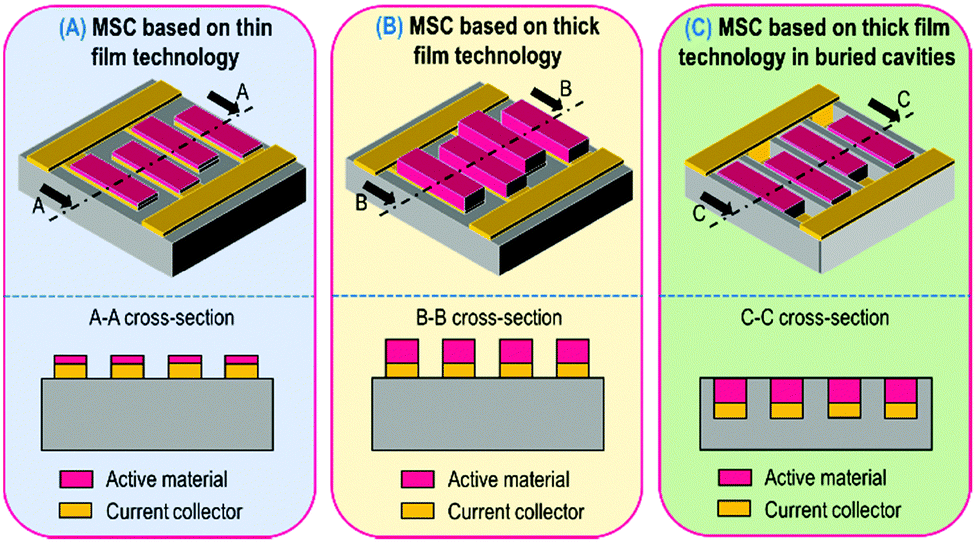 | ||
| Fig. 2 Comparison between thin (A) and thick (B) film technologies for MSC. Only the film thickness is increased to move from the 1st to the 2nd class of technology. (C) Illustration of the thick film technology where the MSC is buried inside a cavity. | ||
Despite the electron and ion transport limitations resulting in the reduction of the power density, thick technology will be described in this review not only to present the high areal capacitance value obtained with this technology but also to highlight a misunderstanding between thick film based MSC buried in cavities and 3D MSC.
As a matter of fact, numerous papers have been published in the last 5 years where the authors have claimed the fabrication of 3D micro-supercapacitors where deep cavities have been etched in a substrate (Fig. 2C) and filled with a large amount of electrode material to produce a high mass loading electrode. In that case, the topology is similar to the thick film technology: the only difference relies upon the burying of the electrode material in substrate cavities. In no way is the energy density of such MSC improved by a 3D effect but rather by thicker layer electrodes buried into cavities.
Intuitively, thin film based MSC (Fig. 2A) will provide lower capacitive performance than thick film technology (Fig. 2B). Nevertheless, the thin film technology (Table 1) is very attractive due to the ease of material synthesis/deposition, the fabrication methods (lithography and patterning) and the full device integration widely developed in the semiconductor industry allowing rapid upscaling of the technological process. The sputtering technique is a deposition process largely developed for thin films in microelectronics (metals, alloys) as well as in the field of micro-batteries for the deposition of electrodes, electrolyte and packaging layers.59–64 The thickness of the layers typically varies from several nanometres up to 5 μm. The sputtering technique was used in pioneering work on MSC in 2001 by Y. S. Yoon et al. to prepare MSC based on stacked layers56,57,65 inspired by what was widely developed for micro-battery applications at the beginning of the 2000s. In that case, a solid electrolyte (LIPON) is sandwiched between two RuO2 (or tungsten-RuO2, i.e. W-RuO2) electrodes in contact with two Pt current collectors (Fig. 3A). While the capacitive properties are really interesting for MSC applications (an areal capacitance value close to 100 mF cm−2), the low ionic conductivity of the LIPON66,67 limits the rate capability of miniaturized EES devices due to the high ohmic drop. The electrolyte issue – already pointed out in 2001 – is the main technological barrier restraining the technological transfer of the micro-supercapacitor technology from lab scale to pilot production line.
 | ||
| Fig. 3 Overview of thin film based MSC. (A) Pt/W-RuO2/LIPON/W-RuO2/Pt stacked layers deposited by sputtering on a silicon wafer56,57 (W-RuO2 = tungsten RuO2): scanning electron microscope cross section imaging, capacitance retention and the galvanostatic cycling charge/discharge profile. (B) TiC–CDC electrode13 produced by a two-step process (inset: cyclic voltammogram of the electrode in 1 M H2SO4 at 1 and 20 mV s−1). (C) Cross-section analysis (TEM imaging) of sputtered nanoporous vanadium nitride thin films.58 Such imaging at the nanoscale clearly shows the inter and intra-columnar porosities within the VN sputtered thin film. The cyclic voltammograms are depicted in 1 M KOH aqueous electrolyte as a function of the deposition pressure to clearly highlight the tuning of the porosity regarding the process parameters. | ||
In 2013, TiC–CDC electrodes (1.6 μm-thick) issued from the chlorination process24 of sputtered titanium carbide thin films were used for the first time as an electrode of interdigitated MSC but the reported capacitance value is too low (6 mF cm−2) to fulfil the energy requirements of IoT applications. Due to a fine optimization between the sputtering and the chlorination processes of metal carbide layers, TiC–CDC electrodes (5 μm-thick) exhibiting an areal capacitance close to 200 mF cm−2 were reported6,68 in aqueous electrolyte. In that case, the fabrication of nanoporous electrodes is achieved using a two-step process. Until recently, the production of nanoporous electrodes for MSC by sputtering was not investigated despite the publication of porous columnar electrodes69 for solid oxide fuel cells using the pulsed laser deposition technique which is a similar physical deposition tool to sputtering. It is well known that the film morphology of the sputtered layer could be tuned regarding the deposition parameters,70,71 following the Thornton structure zone model. Recently, inspired by previous work,41,42 we have investigated the fine tuning of the porosity of sputtered vanadium nitride (VN) acting as an efficient current collector and pseudocapacitive electrode for micro-supercapacitor applications58 (Fig. 3B). Inter- and intra-columnar porosities are finely tuned to reach the best trade-off between high electrical conductivity and a high surface capacitance value. High performance symmetric VN/VN interdigitated micro-supercapacitors with different mass loadings are fabricated using an easily scalable fabrication technique and successfully tested in aqueous electrolyte. An areal capacitance close to 220 mF cm−2 (3.4 μm-thick) is reported for the sputtered VN electrode (optimized porosity), which is in 2018 the best reported value for MSC based on thin film technology (Table 1). The sputtering technique could also be used to deposit a thicker layer (20 μm) at the expense of high deposition time (growth rate ∼ 1 μm h−1): in that case, the reached performance is out of the scope of this part and will be discussed later when thick film technology will be described.
A variety of methods such as layer by layer72,73 (LbL) for deposition of carbon nanotubes (CNT) or Mn3O4, and electrodeposition or spray coating of Mxene11 (Ti3C2) or multiwall74 CNT are investigated to produce efficient micro-supercapacitors but the surface capacitance reached by the MSC based on these fabrication methods stays lower than 30 mF cm−2 (see Table 1). The combination of two deposition techniques to synthesize the electrodes is described in recent papers. Sputtering and electrodeposition techniques are combined to produce MnO2/gold composite thin film electrodes (1.6 μm-thick) integrated in a symmetric MSC75 while an asymmetric activated carbon/MnO2 MSC32 is proposed based on inkjet printing and electrodeposition techniques (Fig. 4).
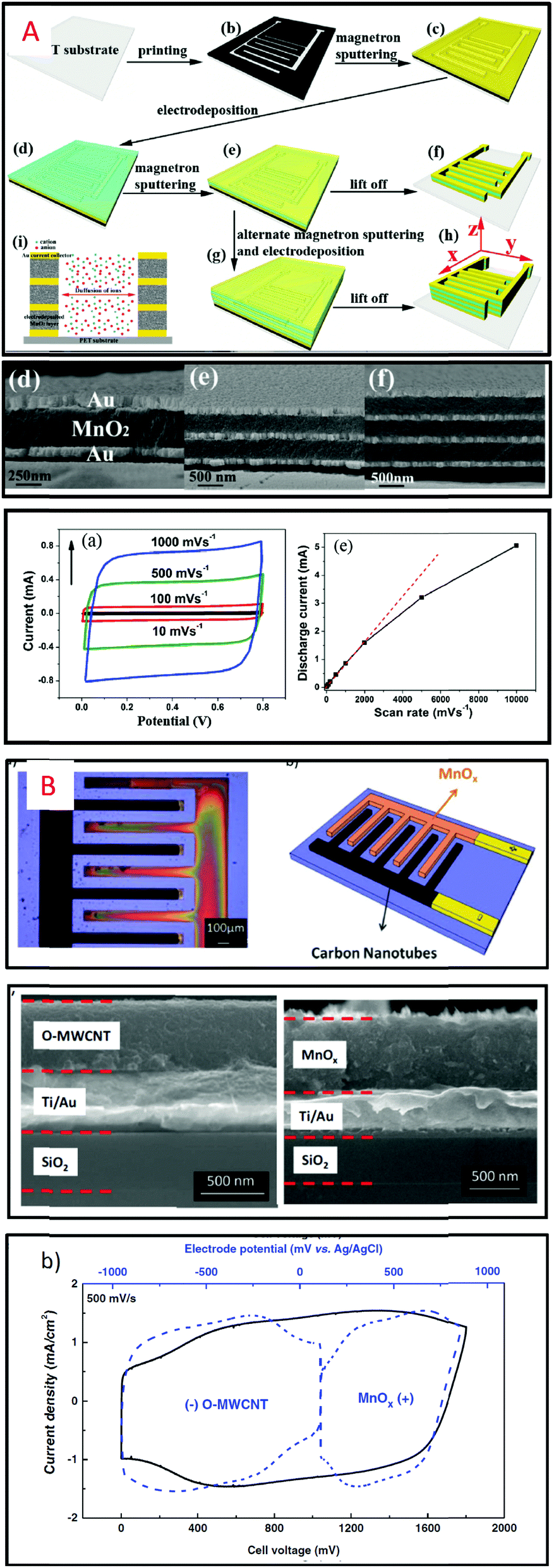 | ||
| Fig. 4 (A) MSC based on thin film technology combining electrodeposition and sputtering to fabricate multilayer composite electrodes and symmetric MSC.75 (B) Electrodeposited MnO2 and inkjet printed activated carbon are deposited on interdigitated Ti/Au current collectors to produce asymmetric MSC.32 | ||
To significantly enhance the surface energy density of MSC, one strategy consists of producing thicker electrodes (Table 2). In that case, deposition techniques used to fabricate miniaturized devices are derived from powder based technology. The main difficulty resides in preventing a short circuit between the two electrodes during the deposition process mainly due to the small interspacing distance of the interdigitated configuration (>5 μm) and the low resolution of the powder based fabrication methods. The solution deposition method76–79 is widely developed in the field of MSC. Generally, carbon based powder is dispersed in a solvent to form a viscous paste or a diluted suspension depending on the formulation (use of binder, conductive agent…). The suspension or the paste is used to fill deep cavities80 of the miniaturized interdigitated topology (Fig. 5A): in that case, despite the presence of deep cavities, no 3D effect is highlighted from this topology based only on thick electrodes. To reach this goal, screen printing is a suitable deposition method.80 With this remark, this review aims at pointing out a misunderstanding in the field of MSC. Electrophoretic deposition from a colloidal suspension31 is another attractive solution to deposit thick layers (5 up to 7 μm-thick) of carbon particles such as activated carbon (AC) or onion like carbon (OLC). Recently, a high energy density asymmetric MSC (74 μW h cm−2) based on 3D inkjet printing was reported:81 as a matter of fact, the printing method is used not only to deposit vanadium based electrodes (400 μm-thick) but also the PVA/LiCl electrolyte (Fig. 5B).
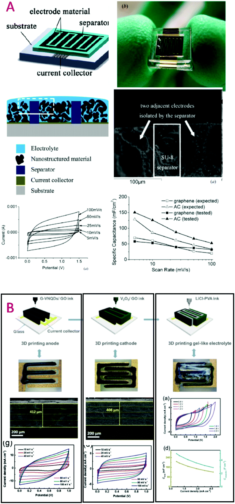 | ||
| Fig. 5 MSC based on thick film technology. (A) Carbon electrodes deposited by the solution injection technique within the SU8 cavity. (B) Graphene/vanadium nitride quantum dots and V2O5/graphene oxide electrodes deposited on interdigitated current collectors by inkjet printing. The gel electrolyte (PVA/LiCl) of the asymmetric MSC is also deposited by this printing method. | ||
The mass loading of the printed electrodes is evaluated close to 3 mg cm−2, i.e. at the same order of magnitude of bulky electrodes. Such mass loading limits the power performance of the asymmetric MSC (<4 mW cm−2).
Despite the attractive energy density reached by the thick film based MSC configuration, the main limitation deals with the rate capabilities of the thick electrode if material showing low electronic conductivity is used as the active layer without the help of electronically conducting agents. The interspacing resolution is another important issue which limits the technological transfer of the technology from lab prototyping to large scale deployment.
An attractive way to significantly improve the energy densities of MSCs when the footprint area is limited as in miniaturized devices is to improve the surface to volume ratio.
Thin film deposition on 3D scaffolds3,82–85 leads to the fabrication of high specific area electrodes with enhanced capacitance properties while keeping high the rate capability of the electrode due to the restricted thickness of the thin film electrodes. When the active layer is step-conformally deposited on a 3D scaffold exhibiting a high area enhancement factor (AEF), the areal capacitance of the 3D MSC is significantly improved at least by one order of magnitude compared to the planar geometry. To fabricate very efficient 3D scaffolds, top down and/or bottom up techniques compatible with semiconductor-based processing have to be used. For each approach, the area enhancement factor (i.e. the projected area per footprint area) could be as high as 100, meaning that a 1 mm2 footprint leads to a 100 mm2 projected area. By combining top down and bottom up techniques to fabricate high performance 3D scaffolds, an AEF higher than 1000 could be obtained. To demonstrate the potentialities of the 3D technology, some assumptions are considered. A symmetric planar interdigitated MnO2/MnO2 MSC (400 nm-thick, 40 mF cm−2 per electrode, cell voltage = 0.9 V) exhibits an energy density close to 1 μW h cm−2. If the same thickness of MnO2 is deposited on a 3D interdigitated scaffold exhibiting an AEF close to 1000, the energy density is improved by three orders of magnitude to reach 1 mW h cm−2. Such a value is similar to the energy density reached by commercially available micro-batteries.86 Comparatively, the best areal energy densities8,9,12,13 reached by 3D MSC are in the range 0.03 to 0.1 mW h cm−2.
4.2. Micro-supercapacitors with 3D architectures
As previously mentioned, the main bottleneck of MSCs deals with the limited energy density stored in the miniaturized EES devices to power sensors for IoT applications. The 3D concept of electrochemical energy storage systems has been studied for more than 15 years for micro-batteries4,5,82,87–90 where the main challenge consists of the fabrication of 3D Li-ion all solid state micro-batteries. Despite many research efforts, the challenge is quite high due (i) to the difficulty to fabricate efficient 3D architectures with high area enhancement factors and (ii) to the conformal deposition of active material on the 3D template. Planar and 3D micro-batteries are built from a stacked configuration where each layer of the micro-device is deposited on the top of each other, from the current collector to the first electrode (positive or negative one), the solid electrolyte, the second electrode, its current collector and the packing layer.Due to the electrolyte issue for MSC (solid electrolyte with high ionic conductivity), the stacked configuration is not a suitable solution not only for planar MSC (as explained in the first part of this review) but also for a 3D point of view. 3D MSC exhibiting a parallel plate topology12 are an alternative solution despite the poor integration from a microelectronic point of view where parallel or series connection of several MSC (elementary cell) using a collective fabrication technique is not possible. In the same way as for thin and thick film configurations, only interdigitated topologies with 3D functionality exhibit the advantages of system integration (miniaturization), and the ease of parallel and series connection, although the energy density is half the one reached by the parallel plate configuration. The development of specific area with 3D templates is widely studied: depending on the dimensions of the 3D scaffold, nano or micro-structured architectures (Fig. 6) are investigated for MSC applications, each of them with their advantages and drawbacks. From a process point of view, nano-architectured or micro-structured interdigitated current collectors (Fig. 6A and C) are firstly fabricated based on bottom up synthesis (nanoscale template) or top down approaches (micrometer scale scaffold). Once the 3D interdigitated template is fabricated, the active material is deposited on the scaffold to achieve symmetric or asymmetric 3D MSCs (Fig. 6B and D). Nevertheless, while the fabrication of 3D MSC is interesting from an energy density point of view, it should be noted that the use of a 3D scaffold may increase the electrical resistance of the 3D MSC. Indeed, taking into account interdigitated electrodes, the ionic pathway between two interpenetrating fingers is higher for planar electrodes than the one for 3D electrodes. Consequently, the areal electrical resistance of the 3D MSC should be increased compared to the 2D electrode design.
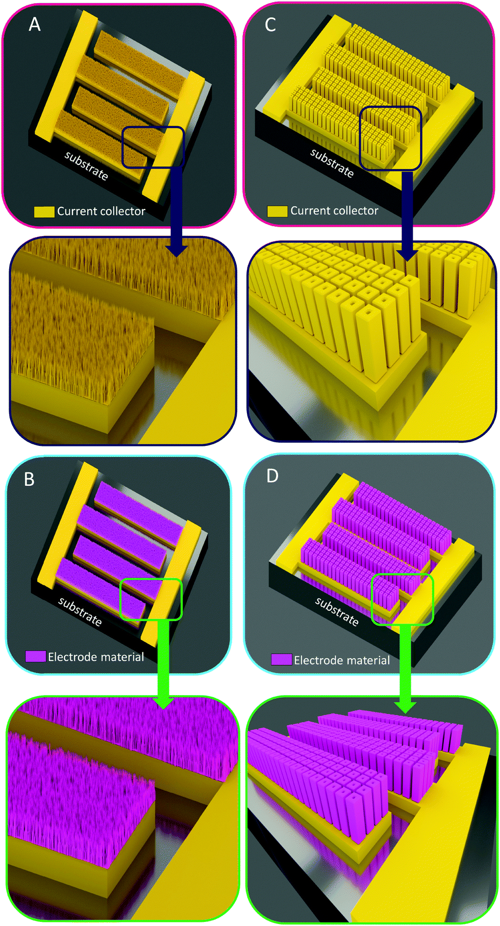 | ||
| Fig. 6 Overview of the 3D architectures used to enhance the energy density of MSC: from nano to micro-structured scaffolds. (A) The nano-architectured current collector of MSCs based on interdigitated topologies is coated with the active material (pink layers, B). In that case, the amount of active material is thickness limited due to the low spacing between two nanostructures (typically less than 50 nm) whereas the specific area of this nanoscale technology is high. (C) Micro-structured current collector in an interdigitated 3D MSC configuration based on micro-tube technology.8 (D) Active material deposited on the 3D micro-tube current collector. In this configuration, the thickness of the electrode material is higher than nanoscale technology (larger spacing between two microstructures) and the fabricated 3D electrodes are robust from a technological point of view. | ||
A large variety of nanostructured templates such as nanowires, nanorods, nano/meso porous templates, and nanosheets/nanowalls are investigated for MSC applications. Since a significant increase of the energy performance is expected, this AEF should reach a higher value (typically, more than 50, meaning that a 1 mm2 footprint area MSC develops an effective surface close to 50 mm2). Such an AEF makes nanostructured 3D templating really interesting, but suffers from either a lack of space between two nanostructures (nanowires) to achieve the conformal deposition of a significant amount of active material, or from a lack of robustness. This last point is a main drawback that severely hinders the technological transfer toward the pilot production line. The lack of space previously pointed out is also meaningful for porous ordered templates when the quantity of deposited material is limited by the pore size diameter.
Subsequently, a micro-structured vertically aligned 3D scaffold is an attractive solution from a robustness point of view. Moreover, the geometrical parameters could be finely tuned to allow the deposition of electrode materials exhibiting a significant thickness (0.5 to 1 μm per electrode) while keeping high the AEF at the same level of magnitude as the 3D nano-architectured scaffold. The design of 3D MSC is a finely tuned trade-off between specific area, material thickness, robustness and the targeted technological readiness level.
To optimize the performance of the 3D based EES miniaturized devices, it is crucial to predict the AEF of the 3D scaffold. The diameters of the 3D structures and the spacing between two structures should be tuned to fulfill these requirements. Taking into account a straight 3D template and, from a mathematical point of view, the AEF of a tubular topology is given by eqn (4):
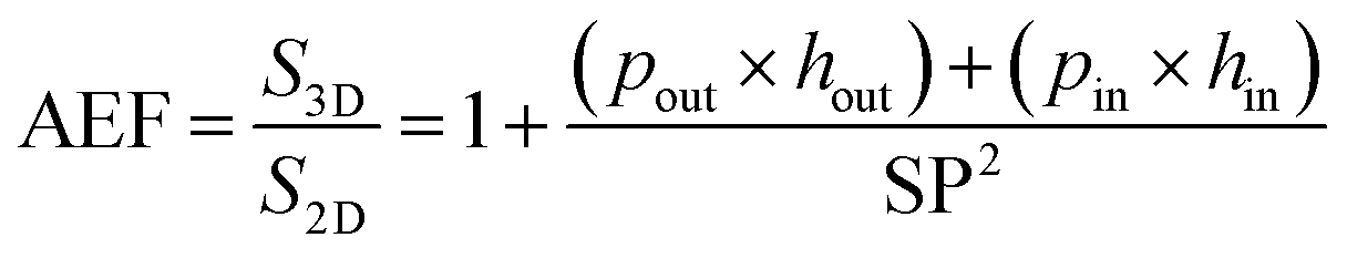 | (4) |
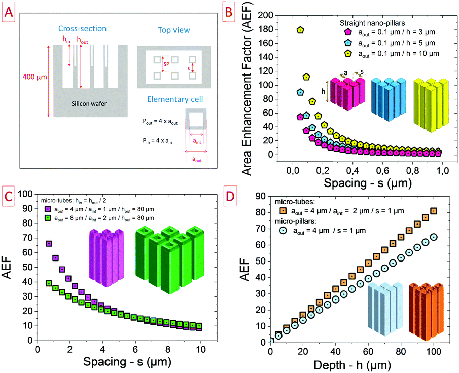 | ||
| Fig. 7 Numerical modelling of the area enhancement factor (AEF) as a function of the geometrical parameters of the 3D scaffold. (A) Overview of the 3D scaffold parameters and shape (top view and cross-section). (B) Evolution of the AEF vs. the spacing parameter for the nanometre-scale template exhibiting 3 different depths (1, 5 and 10 μm). Not surprisingly, the deeper the scaffold, the higher the AEF. (C) AEF vs. the spacing parameter for 2 micro-tube scaffolds exhibiting double dimensions. (D) Area gain as a function of the depth of the scaffold for micro-pillar and micro-tube topologies. | ||
The geometrical parameters of a micro-tube topology (square shape) are reported in Fig. 7A. During the fabrication process of the silicon microtubes, the etched rate of the outer surface is twice faster than the inner surface justifying the shape of the cross-section presented in Fig. 7A. As it is reported in Fig. 7B, the spacing between two structures as well as the depth of the structure are key parameters to maximize the AEF.
Regarding nanopillars (nanowires or nanorods − diameter = 100 nm), the deeper the template, the higher the AEF. Moreover, reducing the spacing between two nanopillars improves the density of the template, i.e. the number of pillars per square centimetre. Consequently, the AEF is maximized close to 180 for a compact and deep 3D nanosized scaffold. At the nanoscale, flexibility is a technological barrier limiting the depth/height of the template. Nevertheless, a compromise has to be found between maximizing the AEF and keeping enough spacing between two nanostructures to allow the deposition of the electrode material. This rationale could be easily translated to micro-sized scaffolds as shown in Fig. 7C where the plots exhibit a similar shape regarding the spacing parameter. When the dimension of the elementary microstructure is double, the AEF performance is significantly reduced at low spacing (below 4 μm – green plot).
Fig. 7D clearly shows the superior performance of the microtube topology as compared to micropillars when regarding similar dimensions. The deeper the microstructures, the better is the AEF. The areal capacitance and so the surface energy density of MSC are exacerbated owing to the AEF of the 3D scaffold.
However, in order to really observe a 3D enhancement of the surface capacitance, the deposited electrode material should not completely fill the specific surface of the template due to a non-suitable deposition technique. Once the 3D scaffold is finely designed, a key issue deals with the conformal deposition of the electrode material layer on this template. To reach this goal, a few deposition methods can be selected (Table 3). Chemical vapor deposition of a carbon layer (2 nm-thick) has been achieved on silicon nanowires26 (120 μm-depth). The surface capacitance is close to 325 mF cm−2 owing to the deep nanostructured template whereas the layer thickness is very low due to the reduced spacing between the flexible nanowires. Among the variety of deposition techniques, electrodeposition is one of the best methods to achieve the conformal deposition of electrode material layers onto a 3D scaffold. This deposition method is used not only for pseudocapacitive metal oxide materials8,9,12,43,84,91–93 such as MnO2 and RuO2 but also for the deposition of conductive polymers43,94–96 such as polyaniline (PANI) and polypyrrole (PPy). 3D interdigitated MSC8,84 based on silicon microtubes or micropillar scaffolds are successfully fabricated at the wafer level using a collective fabrication process with an areal energy density close to 15 μW h cm−2 while keeping high the power performance (>10 mW cm−2). Based on this technology, the reported electrode capacitance varies between 0.5 and 0.7 F cm−2, depending on the geometrical parameters of the scaffold and the thickness of the electrodeposited MnO2 layer (less than 500 nm-thick). Laser scribed graphene (LSG) is a suitable conductive scaffold for 3D MSC. Based on the published results33,97,98 on symmetrical planar LSG/LSG or LSG/RuO2 interdigitated MSCs, R. Kaner and co-workers have focused9 on the design of asymmetric LSG/MnO2 MSC. Based on a 15 μm-depth LSG scaffold coated with 1 μm-thick MnO2 thin film, the as-fabricated asymmetric MSC delivers an areal energy density close to 40 μW h cm−2 while the power performance is restricted due to the low electronic conductivity of the 1 μm-thick MnO2 layer.
In 2015, a high energy density 3D MSC in the parallel plate configuration was published12 by A. Ferris et al. showing for the RuO2 electrode a capacitance of 3.4 F cm−2, thanks to the combination of a macroporous gold scaffold (80 μm-depth) and deposition of thick RuO2 layers by the electrodeposition method. This original approach leads to a high areal capacitance electrode but the rate capability of the electrode is affected by the thickness of the RuO2 layers, limiting the sweep rate (up to 20 mV s−1) and the time duration (15 minutes) of the charge/discharge cycle (Fig. 8A).
 | ||
| Fig. 8 Overview of lab scale prototypes of 3D MSC. (A) RuO2 electrodeposited on a macroporous gold template in the parallel plate configuration. (B) Laser scribed graphene (LSG)–MnO2 based asymmetric MSC. (C) 3D MSC based on the silicon micro-tube technology and step-conformal electrodeposited MnO2 on the 3D scaffold. | ||
Another deposition method suitable to achieve the conformal deposition of thin film on complex 3D micro or nanoarchitectured scaffolds is the atomic layer deposition technique (ALD). ALD is a powerful technology to deposit thin, pinhole-free and conformal layers on complex substrates.99 Moreover, nowadays, ALD is available from an industrial point of view to deposit thin films on large surfaces (especially in the photovoltaic industry where solar panels with a surface close to 2 m2 are produced100), demonstrating a potential technology transfer compatible with CMOS microelectronic facilities. ALD is a gas phase deposition process based on self-limiting reactions between a volatile precursor and active sites on the surface, enabling control of the thickness at the atomic level. ALD is widely investigated as a suitable technique for micro-battery applications or the surface modification of powder electrodes for large scale battery application.3,5,101–103 Since several layers can be successively deposited by this technique, ALD is investigated to develop electrode materials for supercapacitors:104–108 TiN, VOx and RuO2 are the most developed electrode materials deposited by ALD for MSC. An attractive solution to reach outstanding areal energy density while keeping the rate capability of a MSC high deals with the fabrication of hierarchical electrodes combining several advantages: (i) the robustness and the AEF of the 3D micro-structured template acting as the trunk of the micro-tree, (ii) the AEF of the nano-structured scaffold serving as the branch, taking into account a limited length of the nanostructures, and (iii) the deposition of a thin film electrode (typically, less than 100 nm) to produce an efficient template for the development of high energy and high power MSC.
4.3. Prospects in the design of high performance MSC: towards the fabrication of hierarchical electrodes
The hierarchical electrode for MSC concept is reported in Fig. 9. This concept is inspired by the work performed109 by R. Ghodssi on hierarchical electrodes for micro-battery applications. The conductive hierarchical and interdigitated scaffold consists of several interpenetrating fingers decorated with an array of micro-trees combining both the area gain of a 3D micro-structured scaffold and nano-architectured scaffolds (Fig. 9A–C).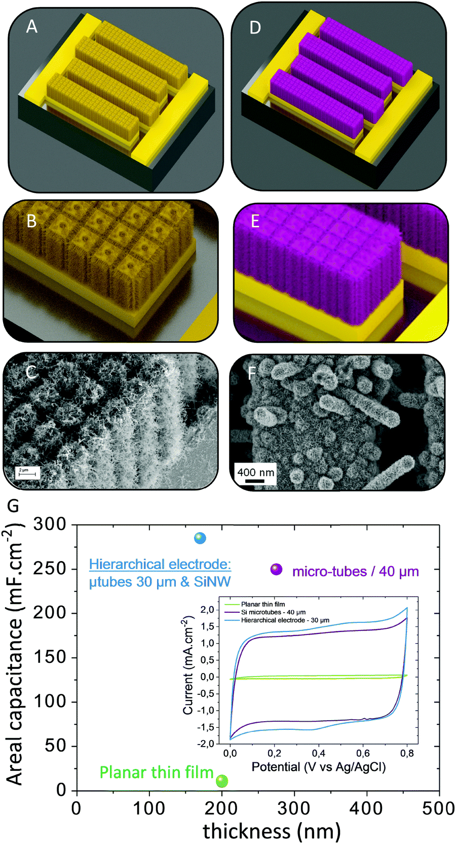 | ||
| Fig. 9 3D MSC based on hierarchical electrodes combining a top down micro-structured scaffold decorated with bottom up nanoscale structures. (A and B) 3D interdigitated current collector. (C) Hierarchical scaffold based on Si micro-tubes and silicon nanowires. (D and E) MSC based on the hierarchical topology and interdigitated configuration. (F) Hierarchical MnO2 electrode. (G) Electrochemical analysis in 0.5 M Na2SO4 at 20 mV s−1. | ||
The electrode material layer is then deposited on this hierarchical template (Fig. 9D–F). Following this concept, 3D silicon micro-tube arrays fabricated using a top down approach have been decorated with silicon nanowires synthesized by a bottom up vapor liquid solid process (Fig. 9E). A 30 nm-thick Pt layer is deposited by ALD on the silicon hierarchical scaffold to provide electronic conductivity to the 3D template. MnO2 thin film (175 nm-thick) is then electrodeposited by a pulsed potentiostatic technique on the hierarchical micro-tree template. Electrochemical characterization is reported in Fig. 9G in 0.5 M Na2SO4 at 20 mV s−1: a comparison is achieved between planar, straight 3D silicon micro-tubes and hierarchical electrodes as a function of the film thickness. The material mass loading is significantly increased by the 3D structures. This is the first conclusion of this work when the 3 CVs are compared. Consequently, the areal capacitance of the 300 nm-thick MnO2 layer on 40 μm depth Si micro-tubes reaches 250 mF cm−2 at 20 mV s−1. Further improvement of the areal capacitance is observed when the 30 μm-depth micro-tube array is decorated with silicon nanowires coated with a 175 nm-thick MnO2 layer. In this case, the measured capacitance is close to 300 mF cm−2, i.e. 20% higher than the one measured on straight deeper micro-tubes, thus demonstrating the pertinence of this strategy for MSC.
5. Electrolyte for micro-supercapacitors
Several features determine good electrolytes: for the sake of high energy storage, at first should come ionic conductivity and the electrochemical window. Water based electrolytes will be limited to ∼1.2 V (depending on the nature of the electrodes), while organic based electrolytes could allow ∼2.8 V and ionic liquid (IL) based electrolytes may reach ∼4 V. The operating temperature range needed will also be a key parameter for selecting an electrolyte since temperature will have effect on ionic conductivity and viscosity, and may induce degradation and vaporization. Moreover, a decrease of the temperature may induce liquid-to-solid state or glass phases transitions. This last parameter refers mostly to the physical state of the electrolyte: it is highly desirable to have solid electrolytes in order to limit the packaging and, most often, safety issues.5.1. Aqueous & organic solvents, and salts
Aqueous electrolytes have been extensively studied since they are cheap and easy to use, but are rather limited due to rather small electrochemical windows, and also due to their possible vaporization and solidification.16,110,111 Often, aqueous acidic H2SO4 or alkali KOH electrolytes are studied and provide at 25 °C ionic conductivities of about ∼1 or 0.6 S cm−1 for 1 M H2SO4 and 6 M KOH respectively. Such 1 M H2SO4 electrolytes were shown to provide the highest capacities for EDLC with carbon electrodes112 (up to 300 F g−1). Moreover, they are also efficient for pseudocapacitive materials, either functionalized carbons or oxides such as MnO2 or RuO2, showing capacitances113 up to 1000 F g−1. Nevertheless, some neutral aqueous solutions, with lithium, sodium, potassium sulphate or cholinium chloride salts, showed slightly enhanced potential windows,114,115 up to ∼2.2 V.Organic electrolytes, e.g. based on acetonitrile (ACN) or propylene carbonate (PC) with 1 M tetraethylammonium tetrafluoroborate (Et4N BF4), are now commonly used in commercialized symmetric carbon based electrochemical capacitors thanks to their electrochemical window at ∼2.8 V.36,116 Nevertheless, ACN or PC with 1 M Et4N BF4 present ionic conductivities at room temperature (RT) around 0.06 or 0.01 S cm−1 respectively, which is lower than that of water based electrolytes. Other nitrile based solvents such as mononitrile butyronitrile (BTN), or dinitrile solvents glutaronitrile (GTN) and adiponitrile (AND) are studied since they provide wider electrochemical windows. Often, these last solvents show conductivities lower than that of ACN based, although the BTN-based solvent presents a conductivity117 at RT around 0.02 S cm−1. The salts chosen for the ionic conduction in these organic solvents are also prone to influence the properties of electrolytes. The cation of Et4N BF4 salt in PC was shown to be intercalated into graphite, thus limiting the operating cell voltage.118 Replacement with Pyr14 BF4 salt allowed a cell voltage around 3.2 V to be reached, as well as better capacitance retention thanks to lower ion intercalation in electrodes. This last salt is also a good example of a variable (here, a high amount) amount of dissolved salt in a given solvent, inducing a variable effect on the viscosity (here, a low effect) and ionic conductivity, either for PC or with ACN.119,120 The choice of the salt is primordial, besides their electrochemical stability, along with their size as referred of electrode pore.116,121 The temperature behaviour may also vary very differently between different solvents; for instance, it was shown, for a given salt (1 M Et4N BF4), that an electrolyte based on PC shows more important decreasing resistance and capacitance with decreasing temperature than that with ACN.118 Moreover, the salt concentration will have effects on the viscosity and conductivity122 as well as also on the maximum energy, with a threshold effect.123
One of the main issues regarding organic electrolytes lies in safety due to their flammability and vapour tension. They thus require packaging adequate towards managing these hazards. However, it is still desirable to increase the electrochemical window above 2.8 V.
5.2. Ionic liquids
Some features of ionic liquids (ILs) answer these last issues: when chosen adequately, they show very poor flammability and negligible vapour tension.124 They have attracted much attention since they allow one to reach higher voltages, and thus higher energy densities, than water and organic solvents. Electrochemical windows up to 3.6 or 4.0 V have been reported,125,126 while increasing the operating voltage from 2.7 V (organic solvents) up to 3.7 V would lead to a 50% energy storage increase.127 One drawback of ILs is their rather high viscosity and low conductivity, e.g. 0.014 S cm−1 for EMIM BF4 at RT. Nevertheless, at higher temperatures, where organic solvents and water show non negligible vapour tension, ILs will present lower viscosities and higher conductivities, without safety hazards. They thus present opportunities for devices operating at higher temperatures. Due to the trade-off between viscosity, ionic conductivity and the electrochemical stability window, the most often used ILs for supercapacitors are those based, regarding anions, on bis(trifluorosulfonyl)imide (TFSI) or BF4 and, regarding cations, pyrrolidinium and imidazolium.128 Seeing that ILs can often be tailored from a given interesting molecule, redox active electrolytes are being studied and show very good enhancement of the energy.129,1305.3. Gels vs. ionogels
Solid electrolytes are the most desirable for many applications, for the sake of features such as safety, flexibility, and miniaturization. Solid electrolytes are commonly found in the literature as polymer electrolytes or ceramic electrolytes. Ceramic electrolytes for electrochemical capacitors could be either phosphorus–sulphur based131 or alumina based;132 owing to their quite low conductivities (∼1 mS cm−1 at RT), long response time and lack of flexibility,133 they are not often considered. Although polyelectrolytes are thoroughly studied since they could provide single ion conduction, their application to supercapacitors remains limited due to their relatively low conductivities134,135 (∼10−5 S cm−1). Gel polymer electrolytes appear to be the best candidates for all-solid supercapacitors. Gels based on aqueous H2SO4 show conductivities as high as that of non-confined aqueous H2SO4 electrolyte,133i.e. ∼0.7 S cm−1 at RT. Moreover they can present a rather low operating temperature,136 down to −10 °C, which could even be improved by the use of 5 mol kg−1 cholinium chloride aqueous solution.115 Nevertheless, their operating voltage remains limited. Replacement of aqueous acids, e.g. phosphoric acid, by the phosphoric acid ester or cholinium salt leads to an increase of the operating voltage up to 1.3 V or 1.5 V but provides mS cm−1 like conductivities at RT.115,137Obtaining gels with ILs thus allows one to have wider operating voltages as well as good conductivities. For this purpose, the principal approaches are: (i) to mix pre-formed inorganic particles with ILs to obtain a physical gel; (ii) to swell polymers or inorganic monoliths with ILs; and (iii) to polycondense or polymerize the confining network within these ILs directly, thus obtaining chemical gels.138 Whereas physical gels are crushable and present lower amounts of ILs, chemical gels, which provide compliant ionogels, confine larger amounts of ILs in order to better preserve and even enhance the dynamics of the liquid state of ILs.139–142 Such ionogels can be obtained as thin films (10 μm) and flexible membranes, thanks to tuning of the host network features, which can based on silsesquioxane precursors, a mixture of polymer and siloxane, or a polymer143,144 (Fig. 10). Conductivities in the range 1–10 mS cm−1 have been obtained at RT, with operating voltages up to 3.5 V, demonstrated either on 100000 cycles for MSC143 or 1200 cycles for lithium micro-batteries. It is here worth to point out that even with these solid-like electrolytes, MSC time constants almost as short as those of non-confined ILs were obtained, i.e. ∼2 and 8 ms for silicon wires and graphene electrodes, respectively. Such interesting behavior, which could be surprising for viscous liquids such as the studied ILs, appears related to their confinement, and more precisely to the breaking down of interactions between ions in aggregates, present in ILs.140,145
 | ||
| Fig. 10 Ionogel technologies for supercapacitors and MSC. (A) 10 μm ionogel films.144 (B) Flexible ionogel membranes.143 (C) Ionic conductivities of carbonate LP30 electrolyte (open squares), LIPON ceramic (open triangles), and PYR13 TFSI with Li salt (orange circles) and ionogels obtained by confinement of this electrolyte within different host networks, i.e. mesoporous silica (red circles), hybrid PVDF–silica (blue squares), and cellulose–silica (orange circles). | ||
5.4. Solving the packaging issue to produce solid state micro-supercapacitors
Several routes for shaping ionogels for micro-devices have been presented. When a sol–gel route is used, simple drop casting can be carried out, as shown for micro-supercapacitors97,146,147 as well as for micro-batteries138 (Fig. 11). Further transferable technology can be developed by means of spin coating and ink-jet printing.148,149 Shaping of polymer based ionogels can also be reached by solution casting or electrospinning after polymer solubilization, with or without a simultaneous sol–gel process.138,150 Starting from monomers, a fast UV-curing process was also shown to be very efficient.151 All together this shaping allows easy packaging of the device, which does not suffer from vapor pressure, and which can moreover sustain a few seconds of reflow soldering.143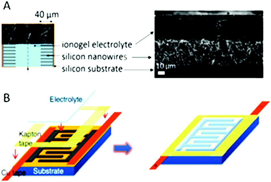 | ||
| Fig. 11 Integration of ionogel in micro-supercapacitors based on parallel plate or interdigitated topologies. (A) Ionogel obtained after drop casting onto a 40 μm long silicon nanowire carpet, assembled face-to-face; the ionogel is formed down to the bottom of the wires and forms simultaneously the solid electrolyte separator.143 (B) Ionogel cast onto interdigitated electrodes.97 | ||
6. Conclusions and outlook
Miniaturized sensor nodes are widely investigated to be implemented within a Wireless Sensor Network (WSN) for the internet of things. As mentioned in the present paper, powering these nodes is still challenging due to the miniaturization of such devices154,155 as well as the surface-limited energy and power densities of available micro-power sources. In practice, the most commonly used power sources to get autonomous such nodes are primary batteries but they are not an attractive solution to propose maintenance free WSN. To address this last issue, the electrochemical energy storage system should be combined with an energy harvesting system. Commercial off the shelf (COTS) node platforms such as IMote 2 from Crossbow156 or other WSN platforms157 integrate a primary or a secondary battery, depending on the combination with an energy harvesting system. In that case, the wireless sensor node exhibits a size close to 4.8 × 3.6 cm2 and more than 10 mW power consumption: long range application (30 m) is achieved within the Industrial Scientific and Medical (ISM) frequency band using the Zigbee protocol, i.e. at 2.4 GHz, and transmits the data at 250 kbps. Regarding the size of the devices and the reported power consumption, powering the Imote 2 node with miniaturized electrochemical energy storage such as COTS micro-batteries or MSC prototypes is still difficult despite the integration of ultra-low power electronic devices in the sensor. Recently, significant improvements were made in the fabrication of cubic-millimeter energy-autonomous wireless sensor nodes152 for health monitoring applications such as intraocular pressure monitoring in the case of glaucoma disease. The Michigan Micro-Mote M3 microsystem exhibits a 3 mm2 footprint area and integrates the pressure sensor, the analog to digital conversion and processing unit, a radiofrequency transceiver and an energy unit composed of a thin film micro-battery and a miniaturized solar cell as depicted in the schematic shown in Fig. 12A. A picture of the M3 micro-mote and the M3 HT evolution153 towards other applications in severe corrosive and high temperature environments is shown in Fig. 12B. The M3 HT system is an enhancement of the previously reported Michigan Micro Mote (M3). In that case, such miniaturized and smart sensors fit perfectly with internet of things applications. While the integration of 3D MSC and COTS micro-batteries is questionable for powering the Imote 2 sensor exhibiting a large footprint area higher than 17 cm2, it makes sense to power the M3 micro-mote (3 mm2) with such electrochemical energy storage micro-devices. Regarding the evolution of the power consumption as a function of the operating time reported in Fig. 12C, three different phases are identified: the measurement phase, the sleep mode and the transmission phase. The pressure measurements are achieved during 19.2 s every 15 minutes (sleep mode): these two time constants are compatible with the one of micro-batteries. The transmission of the accumulated data is performed daily within the ISM band at 433 or 900 MHz: such wireless data transmission requires a peak power close to 48 mW during 0.13 ms which could not be directly provided by a micro-battery. In ref. 152, a 1.6 nF capacitance acts as a local power supply. Nevertheless, the time duration of the data transmission is similar to the time constant of micro-supercapacitors.10,19,33 While the high areal power density of the MSC technology seems initially attractive, the energy density remains the most critical parameter for IoT nodes thereby limiting the implementation of MSC for many IoT applications. If the areal energy density of the MSC is significantly improved based on the 3D technologies described in this review paper, 3D MSC could be used not only during the transmission but also during the measurement phase. In that case, the 3D MSC acts as a buffer miniaturized power source for the micro-battery which extends its cycle life and the lifetime of the small sensor before needing to be recharged with the harvested solar energy. Moreover, as shown for the M3 HT micro mote, microdevices operating in harsh conditions (temperature, pressure) are needed.153 It is thus a challenge to provide miniaturized power sources for designing autonomous smart sensors. However, COTS micro-batteries are not designed to support such harsh conditions. To fulfill the energy requirements in harsh environments, MSC based on ionogel solid electrolytes are an attractive alternative solution to the Cymbet micro-batteries.153 Along with the design of electrodes with lower footprint, solid electrolytes such as ionogels should answer this demand since thermally stable host networks are available, and since confined ionic liquids have already been operated at high temperatures, e.g. up to 120 °C for fuel cells158 or up to 130 °C for waste heat harvesting.127 Moreover, MSC based on ionogel technologies143 have demonstrated the ability to support the reflow soldering process at 250 °C, one of the main important microelectronics processes to attach surface mount devices to printed circuit boards.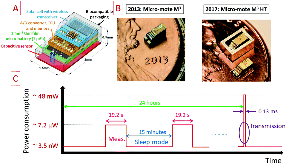 | ||
| Fig. 12 Overview of the miniaturized sensor nodes for IoT applications. (A) Schematic of the Michigan Micro Mote152 (M3) exhibiting a 3 mm2 footprint area. (B) Images of the M3 and M3 HT micro motes.152,153 (C) Evolution of the power consumption of the M3 node during 24 hours. | ||
Emerging IoT applications for health, environmental or industrial monitoring, drug delivery, transportation or wearable personal electronics require integrated and miniaturized electrochemical energy storage systems. To fulfill the energy requirement, micro-supercapacitor technology is widely investigated but up to now there are no MSCs commercially available. While micro-supercapacitors exhibit high power density and large cycle life, the energy density is limited when the footprint area is restricted to several millimeters square. In order to improve the areal energy density of MSCs while keeping constant the footprint area, the current trend is to fabricate 3D micro-supercapacitors with remarkable energy density, i.e. where the areal capacitance of the electrodes is comparable to the one reached by bulky electrodes. Nevertheless, the enhancement of the technological readiness level of such MSC must take into account the collective fabrication of MSC at the wafer level and subsequently process compatibility with MEMS technology instead of lab prototyping. The main technological breakthrough slowing the technological transfer toward the pilot production line relies upon the fabrication of solid state MSC. As no standardization is available for reporting the performance of MSC, several key parameters have to be mentioned to compare the submitted results with state of the art values:
– MSC topology: parallel plate or interdigitated.
– Class of MSC: based on thin film, thick film or 3D technology.
– Thickness of each layer (μm): substrate, current collectors and electrode. The thickness of the electrolyte could be mentioned if solid state devices are proposed.
– Surface (areal) capacitance (mF cm−2) of the electrode and the MSC at different sweep rates or current densities. This value could be normalized regarding the thickness of the electrode (mF cm−2 μm−1) to have a better understanding of the intrinsic properties of an electrode and to compare the reached performance of different electrode materials.
– Areal energy and power densities with true performance metrics (μW h cm−2 and mW cm−2). These densities could be normalized regarding the thickness of the electrode to quantify the amount of active material (μW h cm−2 μm−1 and mW cm−2 μm−1).
– Capacitance retention of the MSC as a function of the number of cycles (cycle life). The sweep rate or the current densities used to measure the MSC performance have to be mentioned and should be on the same order of magnitude as the ones classically used for power devices.
This paper aims at defining the main guidelines and technological roadmap to produce high energy density MSC without sacrificing the power capabilities and taking into account the collective fabrication of the devices at the wafer level. The 3D MSC technology is an attractive solution to power IoT devices in the future.
Conflicts of interest
There are no conflicts to declare.Acknowledgements
This research is financially supported by the ANR within the DENSSCAPIO project (ANR-17-CE05-0015-02). The authors also want to thank the Ministère de l’Enseignement Supérieur et de la Recherche, Région Hauts de France, FEDER and the French network on electrochemical energy storage (RS2E) for the financial support. The French RENATECH network is greatly acknowledged for the use of microfabrication facilities. The authors want to thank Anne Callewaert for the sketch of the 3D micro-supercapacitors and Djamila Hourlier for the growth of silicon nanowires on 3D micro-structures.Notes and references
- A. Whitmore, A. Agarwal and L. Da Xu, Inf. Syst. Front., 2015, 261–274 CrossRef.
- L. Atzori, A. Iera and G. Morabito, Comput. Networks, 2010, 54, 2787–2805 CrossRef.
- M. Létiche, E. Eustache, J. Freixas, A. Demortière, V. De Andrade, L. Morgenroth, P. Tilmant, F. Vaurette, D. Troadec, P. Roussel, T. Brousse and C. Lethien, Adv. Energy Mater., 2017, 7, 1–12 Search PubMed.
- L. Baggetto, R. A. H. Niessen, F. Roozehoom and P. H. L. Notten, Adv. Funct. Mater., 2008, 18, 1057–1066 CrossRef CAS.
- C. Liu, E. I. Gillette, X. Chen, A. J. Pearse, A. C. Kozen, M. A. Schroeder, K. E. Gregorczyk, S. B. Lee and G. W. Rubloff, Nat. Nanotechnol., 2014, 9, 1031–1039 CrossRef CAS PubMed.
- P. Huang, C. Lethien, S. Pinaud, K. Brousse, R. Laloo, V. Turq, M. Respaud, A. Demortière, B. Daffos, P. L. Taberna, B. Chaudret, Y. Gogotsi and P. Simon, Science, 2016, 351, 691–695 CrossRef CAS PubMed.
- M. Létiche, K. Brousse, A. Demortière, P. Huang, B. Daffos, S. Pinaud, M. Respaud, B. Chaudret, P. Roussel, L. Buchaillot, P. L. Taberna, P. Simon and C. Lethien, Adv. Funct. Mater., 2017, 27, 1606813 CrossRef.
- E. Eustache, C. Douard, A. Demortière, V. De Andrade, M. Brachet, J. Le Bideau, T. Brousse and C. Lethien, Adv. Mater. Technol., 2017, 1700126 CrossRef.
- M. F. El-Kady, M. Ihns, M. Li, J. Y. Hwang, M. F. Mousavi, L. Chaney, A. T. Lech and R. B. Kaner, Proc. Natl. Acad. Sci. U. S. A., 2015, 112, 4233–4238 CrossRef CAS PubMed.
- D. Pech, M. Brunet, H. Durou, P. Huang, V. Mochalin, Y. Gogotsi, P.-L. Taberna and P. Simon, Nat. Nanotechnol., 2010, 5, 651–654 CrossRef CAS PubMed.
- Y.-Y. Peng, B. Akuzum, N. Kurra, M.-Q. Zhao, M. Alhabeb, B. Anasori, E. C. Kumbur, H. N. Alshareef, M.-D. Ger and Y. Gogotsi, Energy Environ. Sci., 2016, 9, 2847–2854 RSC.
- A. Ferris, S. Garbarino, D. Guay and D. Pech, Adv. Mater., 2015, 27, 6625–6629 CrossRef CAS PubMed.
- P. Huang, C. Lethien, S. Pinaud, K. Brousse, R. Laloo, V. Turq, M. Respaud, A. Demortiere, B. Daffos, P. L. Taberna, B. Chaudret, Y. Gogotsi and P. Simon, Science, 2016, 351, 691–695 CrossRef CAS PubMed.
- M. F. El-Kady and R. B. Kaner, Nat. Commun., 2013, 4, 1475 CrossRef PubMed.
- E. Eustache, R. Frappier, R. L. Porto, S. Bouhtiyya, J. F. Pierson and T. Brousse, Electrochem. Commun., 2013, 28, 104–106 CrossRef CAS.
- P. Simon and Y. Gogotsi, Nat. Mater., 2008, 7, 845–854 CrossRef CAS PubMed.
- T. Brousse, D. Belanger and J. W. Long, J. Electrochem. Soc., 2015, 162, A5185–A5189 CrossRef CAS.
- Y. Gogotsi and P. Simon, Science, 2011, 334, 917–918 CrossRef CAS PubMed.
- M. Beidaghi and Y. Gogotsi, Energy Environ. Sci., 2014, 7, 867 RSC.
- A. Balducci, D. Belanger, T. Brousse, J. W. Long and W. Sugimoto, J. Electrochem. Soc., 2017, 164, A1487–A1488 CrossRef CAS.
- X. Tian, M. Shi, X. Xu, M. Yan, L. Xu, A. Minhas-Khan, C. Han, L. He and L. Mai, Adv. Mater., 2015, 27, 7476–7482 CrossRef CAS PubMed.
- T. Liu, W. G. Pell and B. E. Conway, Electrochim. Acta, 1997, 42, 3541–3552 CrossRef CAS.
- J. Kowal, E. Avaroglu, F. Chamekh, A. Šenfelds, T. Thien, D. Wijaya and D. U. Sauer, J. Power Sources, 2011, 196, 573–579 CrossRef CAS.
- J. Chmiola, C. Largeot, P. L. Taberna, P. Simon and Y. Gogotsi, Science, 2010, 328, 480–483 CrossRef CAS PubMed.
- M. Heon, S. Lofland, J. Applegate, R. Nolte, E. Cortes, J. D. Hettinger, P.-L. Taberna, P. Simon, P. Huang, M. Brunet and Y. Gogotsi, Energy Environ. Sci., 2011, 4, 135–138 RSC.
- J. P. Alper, S. Wang, F. Rossi, G. Salviati, N. Yiu, C. Carraro and R. Maboudian, Nano Lett., 2014, 14, 1843–1847 CrossRef CAS PubMed.
- Z. S. Wu, X. Feng and H. M. Cheng, Natl. Sci. Rev., 2014, 1, 277–292 CrossRef CAS.
- G. Xiong, C. Meng, R. G. Reifenberger, P. P. Irazoqui and T. S. Fisher, Electroanalysis, 2014, 26, 30–51 CrossRef CAS.
- W. Gu and G. Yushin, Wiley Interdiscip. Rev.: Energy Environ., 2014, 3, 424–473 CAS.
- C. Xu, B. Xu, Y. Gu, Z. Xiong, J. Sun and X. S. Zhao, Energy Environ. Sci., 2013, 6, 1388 RSC.
- D. Pech, M. Brunet, H. Durou, P. Huang, V. Mochalin, Y. Gogotsi, P.-L. Taberna and P. Simon, Nat. Nanotechnol., 2010, 5, 651–654 CrossRef CAS PubMed.
- T. M. Dinh, F. Mesnilgrente, V. Conédéra, N. A. Kyeremateng and D. Pech, J. Electrochem. Soc., 2015, 162, 2016–2020 CrossRef.
- M. F. El-Kady, V. Strong, S. Dubin and R. B. Kaner, Science, 2012, 335, 1326–1330 CrossRef CAS PubMed.
- D. Yu, K. Goh, H. Wang, L. Wei, W. Jiang, Q. Zhang, L. Dai and Y. Chen, Nat. Nanotechnol., 2014, 9, 555–562 CrossRef CAS PubMed.
- W. Gao, N. Singh, L. Song, Z. Liu, A. L. M. Reddy, L. Ci, R. Vajtai, Q. Zhang, B. Wei and P. M. Ajayan, Nat. Nanotechnol., 2011, 6, 496–500 CrossRef CAS PubMed.
- C. Largeot, C. Portet, J. Chmiola, P. L. Taberna, Y. Gogotsi and P. Simon, J. Am. Chem. Soc., 2008, 130, 2730–2731 CrossRef CAS PubMed.
- J. Chmiola, G. Yushin, Y. Gogotsi, C. Portet, P. Simon and P. L. Taberna, Science, 2006, 313, 1760–1763 CrossRef CAS PubMed.
- Z. Wu, K. Parvez, X. Feng and K. Müllen, Nat. Commun., 2013, 4, 2487 CrossRef PubMed.
- B. E. Conway, Electrochemical Supercapacitors Scientific Fundamentals and Technological Applications, 1999, pp. 221–257 Search PubMed.
- M. Toupin, T. Brousse and D. Bélanger, Chem. Mater., 2004, 16, 3184–3190 CrossRef CAS.
- R. Lucio-Porto, S. Bouhtiyya, J. F. Pierson, A. Morel, F. Capon, P. Boulet and T. Brousse, Electrochim. Acta, 2014, 141, 203–211 CrossRef CAS.
- D. Choi, G. E. Blomgren and P. N. Kumta, Adv. Mater., 2006, 18, 1178–1182 CrossRef CAS.
- D. P. Dubal, D. Aradilla, G. Bidan, P. Gentile, T. J. S. Schubert, J. Wimberg, S. Sadki and P. Gomez-Romero, Sci. Rep., 2015, 5, 9771 CrossRef CAS PubMed.
- T.-C. Liu, W. G. Pell, S. L. Roberson and B. E. Conway, J. Electrochem. Soc., 1998, 145, 1882 CrossRef CAS.
- G. Lodi, E. Sivieri, A. De Batisti and S. Trasatti, J. Appl. Electrochem., 1978, 8, 135–143 CrossRef CAS.
- S. Had
![[z with combining macron]](https://www.rsc.org/images/entities/char_007a_0304.gif) i-Jordanov, H. Angerstein-Kozlowska, M. Vukovic and B. E. Conway, J. Electrochem. Soc., 1978, 125, 1471 CrossRef.
i-Jordanov, H. Angerstein-Kozlowska, M. Vukovic and B. E. Conway, J. Electrochem. Soc., 1978, 125, 1471 CrossRef. - H. Y. Lee and J. B. Goodenough, J. Solid State Chem., 1999, 144, 220–223 CrossRef CAS.
- M. Toupin, T. Brousse and D. Belanger, Chem. Mater., 2002, 14, 3946–3952 CrossRef CAS.
- A. Achour, R. L. Porto, M.-A. Soussou, M. Islam, M. Boujtita, K. A. Aissa, L. Le Brizoual, A. Djouadi and T. Brousse, J. Power Sources, 2015, 300, 525–532 CrossRef CAS.
- S. Bouhtiyya, R. Lucio Porto, B. Laïk, P. Boulet, F. Capon, J. P. Pereira-Ramos, T. Brousse and J. F. Pierson, Scr. Mater., 2013, 68, 659–662 CrossRef CAS.
- O. Kartachova, A. M. Glushenkov, Y. Chen, H. Zhang and Y. Chen, J. Mater. Chem. A, 2013, 1, 7889 RSC.
- H. Cui, G. Zhu, X. Liu, F. Liu, Y. Xie, C. Yang, T. Lin, H. Gu and F. Huang, Adv. Sci., 2015, 2, 1–12 Search PubMed.
- G. A. Snook, P. Kao and A. S. Best, J. Power Sources, 2011, 196, 1–12 CrossRef CAS.
- T. Brousse, M. Toupin and D. Bélanger, J. Electrochem. Soc., 2004, 151, A614 CrossRef CAS.
- V. Khomenko, E. Raymundo-Piñero and F. Béguin, J. Power Sources, 2006, 153, 183–190 CrossRef CAS.
- Y. S. Yoon, W. I. Cho, J. H. Lim and D. J. Choi, J. Power Sources, 2001, 101, 126–129 CrossRef CAS.
- H.-K. Kim, S.-H. Cho, Y.-W. Ok, T.-Y. Seong and Y. S. Yoon, J. Vac. Sci. Technol., B: Microelectron. Nanometer Struct.–Process., Meas., Phenom., 2003, 21, 949 CrossRef CAS.
- K. Robert, C. Douard, A. Demortière, F. Blanchard, P. Roussel, T. Brousse and C. Lethien, Adv. Mater. Technol., 2018, 1800036 CrossRef.
- D. W. Murphy, P. A. Christian, F. J. DiSalvo, C. Tsang, A. Dananjay, J. Kim, A. Manthiram, H. I. Schlesinger, H. C. Brown, A. E. Finholt, J. R. Gilbreath, H. R. Hoekstra, E. K. Hyde, J. Amer, X. Yu, J. B. Bates, G. E. Jellison and F. X. Hart, J. Electrochem. Soc. Sci., 1997, 144965 Search PubMed; J. Carides and J. V. Waszczak, Inorg. Chem. Chem. Soc., 1997, 144965 Search PubMed.
- N. Balke, S. Jesse, A. N. Morozovska, E. Eliseev, D. W. Chung, Y. Kim, L. Adamczyk, R. E. García, N. Dudney and S. V. Kalinin, Nat. Nanotechnol., 2010, 5, 749–754 CrossRef CAS PubMed.
- J. Li, C. Ma, M. Chi, C. Liang and N. J. Dudney, Adv. Energy Mater., 2015, 5, 1–6 Search PubMed.
- V. P. Phan, B. Pecquenard and F. Le Cras, Adv. Funct. Mater., 2012, 22, 2580–2584 CrossRef CAS.
- M. Létiche, M. Hallot, M. Huvé, T. Brousse, P. Roussel and C. Lethien, Chem. Mater., 2017, 29, 6044–6057 CrossRef.
- T. Pichonat, C. Lethien, N. Tiercelin, S. Godey, E. Pichonat, P. Roussel, M. Colmont and P. A. Rolland, Mater. Chem. Phys., 2010, 123, 231–235 CrossRef CAS.
- J. H. Lim, D. J. Choi, H.-K. Kim, W. Il Cho and Y. S. Yoon, J. Electrochem. Soc., 2001, 148, A275 CrossRef CAS.
- J. B. Bates, N. J. Dudney, B. Neudecker, A. Ueda and C. D. Evans, Solid State Ionics, 2000, 135, 33–45 CrossRef CAS.
- T. Pichonat, C. Lethien, N. Tiercelin, S. Godey, E. Pichonat, P. Roussel, M. Colmont and P. A. Rolland, Mater. Chem. Phys., 2010, 123, 231–235 CrossRef CAS.
- M. Létiche, K. Brousse, A. Demortière, P. Huang, B. Daffos, S. Pinaud, M. Respaud, B. Chaudret, P. Roussel, L. Buchaillot, P. L. Taberna, P. Simon and C. Lethien, Adv. Funct. Mater., 2017, 27, 1–10 CrossRef.
- W. Jung, J. O. Dereux, W. C. Chueh, Y. Hao and S. M. Haile, Energy Environ. Sci., 2012, 5, 8682 RSC.
- J. A. Thornton, J. Vac. Sci. Technol., A, 1986, 4, 3059–3065 CrossRef CAS.
- J. A. Thornton, Annu. Rev. Mater. Sci., 1977, 7, 239–260 CrossRef CAS.
- S. Y. Hong, J. Yoon, S. W. Jin, Y. Lim, S. Lee and G. Zi, ACS Nano, 2014, 8844–8855 CrossRef CAS PubMed.
- Y. Lim, J. Yoon, J. Yun, D. Kim, S. Y. Hong, S. J. Lee, G. Zi and J. S. Ha, ACS Nano, 2014, 8, 11639–11650 CrossRef CAS PubMed.
- D. Kim, G. Lee, D. Kim and J. S. Ha, ACS Appl. Mater. Interfaces, 2015, 7, 4608–4615 CrossRef CAS PubMed.
- H. B. Hu, Z. B. Pei, H. J. Fan and C. H. Ye, Small, 2016, 12, 3059–3069 CrossRef CAS PubMed.
- C. Shen, X. Wang, W. Zhang and F. Kang, J. Power Sources, 2011, 196, 10465–10471 CrossRef CAS.
- J. Pu, X. Wang, T. Zhang, S. Li and J. Liu, Nanotechnology, 2016, 27, 45701 CrossRef PubMed.
- X. Wang, H. Xing, C. Shen and S. Li, Micro Nano Lett., 2012, 7, 1166–1169 CrossRef.
- S. Li, X. Wang, H. Xing and C. Shen, J. Micromech. Microeng., 2013, 23, 114013 CrossRef.
- H. Durou, D. Pech, D. Colin, P. Simon, P.-L. Taberna and M. Brunet, Microsyst. Technol., 2012, 18, 467–473 CrossRef CAS.
- K. Shen, J. Ding and S. Yang, Adv. Energy Mater., 2018, 1800408 CrossRef.
- J. W. Long, B. Dunn, D. R. Rolison and H. S. White, Chem. Rev., 2004, 104, 4463–4492 CrossRef CAS PubMed.
- H. S. Min, B. Y. Park, L. Taherabadi, C. Wang, Y. Yeh, R. Zaouk, M. J. Madou and B. Dunn, J. Power Sources, 2008, 178, 795–800 CrossRef CAS.
- E. Eustache, C. Douard, R. Retoux, C. Lethien and T. Brousse, Adv. Energy Mater., 2015, 5, 3–7 Search PubMed.
- M. Beidaghi and C. Wang, Adv. Funct. Mater., 2012, 22, 4501–4510 CrossRef CAS.
- Cymbet Corporation, Data Sheet, 2010, 1–5 Search PubMed.
- E. Eustache, P. Tilmant, L. Morgenroth, P. Roussel, G. Patriarche, D. Troadec, N. Rolland, T. Brousse and C. Lethien, Adv. Energy Mater., 2014, 4, 1–11 Search PubMed.
- M. Létiche, E. Eustache, J. Freixas, A. Demortière, V. De Andrade, L. Morgenroth, P. Tilmant, F. Vaurette, D. Troadec, P. Roussel, T. Brousse and C. Lethien, Adv. Energy Mater., 2017, 7, 1601402 CrossRef.
- M. Roberts, P. Johns, J. Owen, D. Brandell, K. Edstrom, G. El Enany, C. Guery, D. Golodnitsky, M. Lacey, C. Lecoeur, H. Mazor, E. Peled, E. Perre, M. M. Shaijumon, P. Simon and P.-L. Taberna, J. Mater. Chem., 2011, 21, 9876 RSC.
- C. Lethien, M. Zegaoui, P. Roussel, P. Tilmant, N. Rolland and P. A. Rolland, Microelectron. Eng., 2011, 88, 3172–3177 CrossRef CAS.
- Y. Q. Li, X. M. Shi, X. Y. Lang, Z. Wen, J. C. Li and Q. Jiang, Adv. Funct. Mater., 2016, 26, 1830–1839 CrossRef CAS.
- Z. Su, C. Yang, B. Xie, Z. Lin, Z. Zhang, J. Liu, B. Li, F. Kang and C. P. Wong, Energy Environ. Sci., 2014, 7, 2652–2659 RSC.
- A. Ponrouch, S. Garbarino, E. Bertin and D. Guay, J. Power Sources, 2013, 221, 228–231 CrossRef CAS.
- X. Lang, L. Zhang, T. Fujita, Y. Ding and M. Chen, J. Power Sources, 2012, 197, 325–329 CrossRef CAS.
- M. Beidaghi and C. Wang, Electrochim. Acta, 2011, 56, 9508–9514 CrossRef CAS.
- J. Maeng, Y. J. Kim, C. Meng and P. P. Irazoqui, ACS Appl. Mater. Interfaces, 2016, 8, 13458–13465 CrossRef CAS PubMed.
- M. F. El-Kady and R. B. Kaner, Nat. Commun., 2013, 4, 1475 CrossRef PubMed.
- J. Y. Hwang, M. F. El-Kady, Y. Wang, L. Wang, Y. Shao, K. Marsh, J. M. Ko and R. B. Kaner, Nano Energy, 2015, 18, 57–70 CrossRef CAS.
- S. M. George, Chem. Rev., 2010, 110, 111–131 CrossRef CAS PubMed.
- J. A. van Delft, D. Garcia-Alonso and W. M. M. Kessels, Semicond. Sci. Technol., 2012, 27, 074002 CrossRef.
- J. Liu and X. Sun, Nanotechnology, 2015, 26, 024001 CrossRef CAS PubMed.
- H.-M. Cho, M. V. Chen, A. C. MacRae and Y. S. Meng, ACS Appl. Mater. Interfaces, 2015, 7, 16231–16239 CrossRef CAS PubMed.
- S. Ouendi, C. Arico, F. Blanchard, J. Codron, X. Wallart, P. Louis, P. Roussel, L. Clavier, P. Simon and C. Lethien, Energy Storage Mater., 2018, 1–8 Search PubMed.
- E. Kao, C. Yang, R. Warren, A. Kozinda and L. Lin, Sens. Actuators, A, 2016, 240, 160–166 CrossRef CAS.
- R. Warren, F. Sammoura, F. Tounsi, M. Sanghadasa and L. Lin, J. Mater. Chem. A, 2015, 3, 15568–15575 RSC.
- K. Grigoras, J. Keskinen, L. Grönberg, E. Yli-Rantala, S. Laakso, H. Völimöki, P. Kauranen, J. Ahopelto and M. Prunnila, Nano Energy, 2016, 26, 340–345 CrossRef CAS.
- P. Lu, P. Ohlckers, L. Müller, S. Leopold, M. Hoffmann, K. Grigoras, J. Ahopelto, M. Prunnila and X. Chen, Electrochem. Commun., 2016, 70, 51–55 CrossRef CAS.
- S. Boukhalfa, K. Evanoff and G. Yushin, Energy Environ. Sci., 2012, 5, 6872–6879 RSC.
- K. Gerasopoulos, E. Pomerantseva, M. McCarthy, A. Brown, C. Wang, J. Culver and R. Ghodssi, ACS Nano, 2012, 6, 6422–6432 CrossRef CAS PubMed.
- X. Zang, R. Zhang, Z. Zhen, W. Lai, C. Yang, F. Kang and H. Zhu, Nano Energy, 2017, 40, 224–232 CrossRef CAS.
- R. S. Borges, A. L. M. Reddy, M. T. F. Rodrigues, H. Gullapalli, K. Balakrishnan, G. G. Silva and P. M. Ajayan, Sci. Rep., 2013, 3, 1–6 Search PubMed.
- D. Jiménez-Cordero, F. Heras, M. A. Gilarranz and E. Raymundo-Piñero, Carbon, 2014, 71, 127–138 CrossRef.
- X. Liu and P. G. Pickup, J. Solid State Electrochem., 2010, 14, 231–240 CrossRef CAS.
- K. Fic, G. Lota, M. Meller and E. Frackowiak, Energy Environ. Sci., 2012, 5, 5842–5850 RSC.
- Q. Abbas and F. Béguin, ChemSusChem, 2018, 11, 975–984 CrossRef CAS PubMed.
- J. Chmiola, G. Yushin, Y. Gogotsi, C. Portet and P. L. Taberna, Science, 2006, 7, 1760–1764 CrossRef PubMed.
- A. R. Neale, C. Schütter, P. Wilde, P. Goodrich, C. Hardacre, S. Passerini, A. Balducci and J. Jacquemin, J. Chem. Eng. Data, 2017, 62, 376–390 CrossRef CAS.
- L. J. Hardwick, M. Hahn, P. Ruch, M. Holzapfel, W. Scheifele, H. Buqa, F. Krumeich, P. Novak and R. Kotz, Electrochim. Acta, 2006, 52, 675–680 CrossRef CAS.
- S. Pohlmann and A. Balducci, Electrochim. Acta, 2013, 110, 221–227 CrossRef CAS.
- J. Krummacher and S. Passerini, ChemElectroChem, 2017, 4, 353–361 CrossRef CAS.
- S. Pohlmann, C. R. Castro and A. Balducci, J. Electrochem. Soc., 2015, 162, A5020–A5030 CrossRef CAS.
- M. Ue, Electrochemistry, 2007, 8, 565–572 CrossRef.
- J. Zheng and T. Jow, J. Electrochem. Soc., 1997, 144, 2417–2420 CrossRef CAS.
- M. Armand, F. Endres, D. R. MacFarlane, H. Ohno and B. Scrosati, Nat. Mater., 2009, 8, 621–629 CrossRef CAS PubMed.
- A. Balducci, W. A. Henderson, M. Mastragostino, S. Passerini, P. Simon and F. Soavi, Electrochim. Acta, 2005, 50, 2233–2237 CrossRef.
- C. Arbizzani, M. Biso, D. Cericola, M. Lazzari, F. Soavi and M. Mastragostino, J. Power Sources, 2008, 185, 1575–1579 CrossRef CAS.
- D. R. MacFarlane, N. Tachikawa, M. Forsyth, J. M. Pringle, P. C. Howlett, G. D. Elliott, J. H. Davis, M. Watanabe, P. Simon and C. A. Angell, Energy Environ. Sci., 2014, 7, 232–250 RSC.
- A. Brandt, S. Pohlmann, A. Varzi, A. Balducci and S. Passerini, MRS Bull., 2013, 38, 554–559 CrossRef CAS.
- E. Mourad, L. Coustan, P. Lannelongue, D. Zigah, A. Mehdi, A. Vioux, S. A. Freunberger, F. Favier and O. Fontaine, Nat. Mater., 2016, 16, 446–453 CrossRef PubMed.
- B. Gorska, E. Frąckowiak and F. Béguin, Curr. Opin. Electrochem., 2018, 9, 95–105 CrossRef CAS.
- B. E. Francisco, C. M. Jones, S.-H. Lee and C. R. Stoldt, Appl. Phys. Lett., 2012, 100, 103902 CrossRef.
- A. S. Ulihin, Y. G. Mateyshina and N. F. Uvarov, Solid State Ionics, 2013, 251, 62–65 CrossRef CAS.
- I. Stepniak and A. Ciszewski, Electrochim. Acta, 2011, 56, 2477–2482 CrossRef CAS.
- F. N. Ajjan, M. Ambrogi, A. Tiruye, D. Cordella, A. M. Fernandes, K. Grygiel, M. Isik, N. Patil, L. Porcarelli, G. Rocasalbas, E. Zeglio, M. Antonietti, C. Detrembleur, O. Inganäs, C. Jérôme, R. Marcilla, D. Mecerreyes, M. Moreno, D. Taton and J. Yuan, Polym. Int., 2017, 66, 1119–1128 CrossRef CAS.
- G. Rydzek, Q. Ji, M. Li, P. Schaaf, J. P. Hill, F. Boulmedais and K. Ariga, Nano Today, 2015, 1–30 Search PubMed.
- S. Yamazaki, A. Takegawa, Y. Kaneko, J. Kadokawa and M. Yamagata, J. Power Sources, 2010, 195, 6245–6249 CrossRef CAS.
- A. Ł. Anna, I. A. Rutkowska, P. Taberna, P. Simon and P. J. Kulesza, J. Power Sources, 2015, 274, 1147–1154 CrossRef.
- J. Le Bideau, J. Ducros, P. Soudan and D. Guyomard, Adv. Funct. Mater., 2011, 21, 4073–4078 CrossRef CAS.
- N. Butchtova, A. Guyomard-Lack and J. Le Bideau, Green Chem., 2014, 16, 1149–1152 RSC.
- A. Guyomard-Lack, P.-E. Delannoy, N. Dupré, C. V. Cerclier, B. Humbert and J. Le Bideau, Phys. Chem. Chem. Phys., 2014, 16, 23639–23645 RSC.
- C. Iacob, J. R. Sangoro, W. K. Kipnusu, R. Valiullin, J. Karger and F. Kremer, Soft Matter, 2012, 8, 289–293 RSC.
- A. Guyomard-Lack, B. Said, N. Dupré, A. Galarneau and J. Le Bideau, New J. Chem., 2016, 40, 4269–4276 RSC.
- M. Brachet, D. Gaboriau, P. Gentile, S. Fantini, G. Bidan, S. Sadki, T. Brousse and J. Le Bideau, J. Mater. Chem. A, 2016, 4, 11835–11843 RSC.
- A. Guyomard-lack, J. Abusleme, P. Soudan, B. Lestriez, D. Guyomard and J. Le Bideau, Adv. Energy Mater., 2014, 4, 1301570 CrossRef.
- R. Futamura, T. Iiyama, Y. Takasaki, Y. Gogotsi, M. J. Biggs, M. Salanne, J. Ségalini, P. Simon and K. Kaneko, Nat. Mater., 2017, 16, 1225–1234 CrossRef CAS PubMed.
- L. Negre, B. Daffos, P. L. Taberna and P. Simon, J. Electrochem. Soc., 2015, 162, A5037–A5040 CrossRef CAS.
- M. Brachet, T. Brousse and J. Le Bideau, ECS Electrochem. Lett., 2014, 3, A112–A115 CrossRef CAS.
- D. S. Ashby, R. H. Deblock, C. Lai, C. S. Choi and B. S. Dunn, Joule, 2017, 1–15 Search PubMed.
- P. E. Delannoy, B. Riou, B. Lestriez, D. Guyomard, T. Brousse and J. Le Bideau, J. Power Sources, 2015, 274, 1085–1090 CrossRef CAS.
- A. Taubert, Eur. J. Inorg. Chem., 2015, 1148–1159 CrossRef CAS.
- C. Gerbaldi, J. R. Nair, G. Meligrana, R. Bongiovanni, S. Bodoardo and N. Penazzi, Electrochim. Acta, 2010, 55, 1460–1467 CrossRef CAS.
- G. Chen, H. Ghaed and R. Haque, IEEE Int. Solid-State Circuits Conf., 2011, 138–139 Search PubMed.
- M. Choi, Y. Sui, I. H. Lee, R. Meredith, Y. Ma, G. Kim, D. Blaauw, Y. B. Gianchandani and T. Li, Sensors, 2017, 17, 2190 CrossRef PubMed.
- D. Steingart, S. Roundy, P. K. Wright and J. W. Evans, MRS Bull., 2008, 33, 408–409 CrossRef CAS.
- A. Raj and D. Steingart, J. Electrochem. Soc., 2018, 165, 3130–3136 CrossRef.
- Crossbow, 6020-0117-02 Rev A, 2–4.
- G. A. Al-suhail, J. Mehdi and G. Nikolakopoulos, J. Commun. Technol. Electron. Comput. Sci., 2017, 23–30 Search PubMed.
- T. Yasuda and M. Watanabe, MRS Bull., 2013, 38, 560–566 CrossRef CAS.
- J. H. Sung, S. J. Kim and K. H. Lee, J. Power Sources, 2004, 133, 312–319 CrossRef CAS.
- W. Si, C. Yan, Y. Chen, S. Oswald, L. Han and O. G. Schmidt, Energy Environ. Sci., 2013, 6, 3218 RSC.
- Y. S. Yoon, W. I. Cho, J. H. Lim and D. J. Choi, J. Power Sources, 2001, 101, 126–129 CrossRef CAS.
- J. Xu and G. Shen, Nano Energy, 2015, 13, 131–139 CrossRef CAS.
- P. Huang, M. Heon, D. Pech, M. Brunet, P. L. Taberna, Y. Gogotsi, S. Lofland, J. D. Hettinger and P. Simon, J. Power Sources, 2013, 225, 240–244 CrossRef CAS.
- D. Pech, M. Brunet, P. L. Taberna, P. Simon, N. Fabre, F. Mesnilgrente, V. Conédéra and H. Durou, J. Power Sources, 2010, 195, 1266–1269 CrossRef CAS.
- B. Hsia, J. Marschewski, S. Wang, J. Bin In, C. Carraro, D. Poulikakos, C. P. Grigoropoulos and R. Maboudian, Nanotechnology, 2014, 25, 055401 CrossRef PubMed.
- P. Huang, D. Pech, R. Lin, J. K. McDonough, M. Brunet, P. L. Taberna, Y. Gogotsi and P. Simon, Electrochem. Commun., 2013, 36, 53–56 CrossRef CAS.
- J. Lin, C. Zhang, Z. Yan, Y. Zhu, Z. Peng, R. H. Hauge, D. Natelson and J. M. Tour, Nano Lett., 2013, 13, 72–78 CrossRef CAS PubMed.
- R.-Z. Li, R. Peng, K. D. Kihm, S. Bai, D. Bridges, U. Tumuluri, Z. Wu, T. Zhang, G. Compagnini, Z. Feng and A. Hu, Energy Environ. Sci., 2016, 9, 1458–1467 RSC.
- K. Brousse, P. Huang, S. Pinaud, M. Respaud, B. Daffos, B. Chaudret, C. Lethien, P. L. Taberna and P. Simon, J. Power Sources, 2016, 328, 520–526 CrossRef CAS.
- L. Li, J. Zhang, Z. Peng, Y. Li, C. Gao, Y. Ji, R. Ye, N. D. Kim, Q. Zhong, Y. Yang, H. Fei, G. Ruan and J. M. Tour, Adv. Mater., 2016, 28, 838–845 CrossRef CAS PubMed.
- S. M. Mirvakili and I. W. Hunter, Adv. Mater., 2017, 29, 1–6 Search PubMed.
- C. Shen, X. Wang, S. Li, J. Wang, W. Zhang and F. Kang, J. Power Sources, 2013, 234, 302–309 CrossRef CAS.
- C. Meng, J. Maeng, S. W. M. John and P. P. Irazoqui, Adv. Energy Mater., 2014, 4, 1–7 Search PubMed.
- Z. S. Wu, K. Parvez, S. Li, S. Yang, Z. Liu, S. Liu, X. Feng and K. Mullen, Adv. Mater., 2015, 27, 4054–4061 CrossRef CAS PubMed.
- C. Shen, X. Wang, W. Zhang and F. Kang, J. Power Sources, 2011, 196, 10465–10471 CrossRef CAS.
- D. Aradilla, D. Gaboriau, G. Bidan, P. Gentile, M. Boniface, D. Dubal, P. Gómez-Romero, J. Wimberg, T. J. S. Schubert and S. Sadki, J. Mater. Chem. A, 2015, 3, 13978–13985 RSC.
- T. M. Dinh, A. Achour, S. Vizireanu, G. Dinescu, L. Nistor, K. Armstrong, D. Guay and D. Pech, Nano Energy, 2014, 10, 288–294 CrossRef CAS.
| This journal is © The Royal Society of Chemistry 2019 |