
 Open Access Article
 This Open Access Article is licensed under a
 Creative Commons Attribution 3.0 Unported Licence
Quantum chemical models for the absorption of endohedral clusters on Si(111)-(7 × 7): a subtle balance between W–Si and Si–Si bonding†
Xiao
Jin
,
Vaida
Arcisauskaite
 and
John E.
McGrady
*
and
John E.
McGrady
*
Department of Chemistry, University of Oxford, OX1 3QZ, UK. E-mail: john.mcgrady@chem.ox.ac.uk
First published on 7th June 2019
Abstract
The link between the intrinsic electronic properties of an endohedral metallo-silicon cluster, W@Si12, its ability to bind to a Si(111)-(7 × 7) surface and the impact on transmission properties is explored using periodic density functional theory. The W 5dz2 orbital, the LUMO of the isolated cluster, plays a critical role in all aspects, forming a covalent bond between the metal and the silicon surface, and then providing an effective transmission channel that allows current to flow from the surface to STM tip. The STM images therefore provide a very direct probe of the W–Si surface bond.
Introduction
Many of the recent advances in the field of molecular electronics have been driven by studies of molecules with appropriate linker groups (thiolate, for example) absorbed on metallic surfaces.1 In such circumstances, the boundary between molecule and surface is clearly defined and the effects of surface binding can be viewed as a small perturbation to the electronic structure of the molecule. This assumption is somehow intrinsic to the concept of ‘molecular electronics’ because only in that limit can we hope to interpret current/voltage characteristics based on the properties of the isolated molecule. The integrated chip industry is, however, based on silicon, and there is clearly merit in studying molecules that are compatible with existing CMOS architectures. Molecules that themselves contain silicon are obvious candidates in this regard, and there is a growing body of data on the gas-phase chemistry of endohedral silicon clusters, M@Sin, containing a wide range of transition elements. The fact that some of these clusters are particularly stable in the gas phase for certain ‘magic’ values of n is well established in the literature, courtesy of Beck's original mass spectrometric investigations2,3 and a range of subsequent spectroscopic probes.4 The structures and magnetic properties of these clusters depend critically on the identity of the transition metal, potentially offering a means of tuning the properties of a surface upon which they might be absorbed. Beck's experiments used laser vaporization of a silicon wafer to generate clusters in a molecular beam which is then quenched in the presence of metal carbonyl species to generate cationic clusters with formula [M@Sin]+. The dominant peaks in the mass spectra typically have values of n in the range 14–17, with [WSi15]+ and [WSi16]+ particularly prominent in the experiments performed with W(CO)6. Of more direct relevance to this paper are the complementary experiments carried out by Kanayama, Hiura and co-workers using SiH4, rather than a silicon wafer, as a source of silicon. These experiments generate clusters with general formula [MSinHx]+, which typically contain smaller numbers of Si atoms (n) than observed in Beck's experiments. For example, n varies from 14 for early transition metals such as Hf to 9 in later metals such as Ir. In the case of W, the dominant peak with n = 12 is completely devoid of hydrogens (x = 0), an observation that was interpreted to indicate that the metal atom is endohedrally encapsulated, such that it saturates the valence requirements of all twelve silicon atoms5 (the @ is used from hereon in to indicate an endohedral species). Computational studies on cationic WSin clusters (n = 6–16) suggest that the species such as the [W@Si15]+ ion observed in Beck's experiments are truly ‘magic’ in the sense that they represent a thermodynamic sink.6a The smaller [W@Si12]+ clusters, in contrast, owe their stability to kinetic factors, because further growth would require direct contact between the transition metal and additional molecules of SiH4, and this is prevented by the adoption of the endohedral geometry. Lu and Nagase's study of neutral clusters has also emphasised the relative thermodynamic stability of W@Si16 over W@Si12.6b Nevertheless, the structure and spectroscopy of the M@Si12 family of clusters has been the subject of numerous experimental and computational studies which have established the stability of a hexagonal prismatic geometry for W@Si12 and its isoelectronic analogues Cr@Si12 and [Mn@Si12]+.4c,7 Our own analysis of the electronic structure of this family suggests that residual Si–Si π bonding within the Si12 cage is an important stabilising component,8 and this unsaturation may play an important role in binding to a surface.The motivation for this work was provided by another set of experiments reported by Kanayama and co-workers, where they generated different members of the [TaSinHx]+ series from the reaction of Ta+ ions with SiH4.9 The beam of ions produced contains a mixture of clusters with n = 10–13 and x = 0–6, with the [TaSi10Hx]+ and [TaSi11Hx]+ species the most abundant. The inherent reactivity of these clusters means that crystalline samples remain elusive, but scanning tunneling microscopy (STM) images of the [TaSi10–13Hx]+ clusters deposited on a Si(111)-(7 × 7) surface suggest that at least some of the clusters retain their integrity after surface binding.9 In principle, at least, this represents a top-down approach to the integration of metal atoms into a silicon surface via soft landing of pre-formed gas-phase molecular clusters. Kanayama's STM measurements reveal bright dots on the surface with a narrow range of heights, which were assigned to intact surface-absorbed clusters. The precise geometries of these surface features are not clear, but the authors noted that [Ta@Si12]− is isoelectronic with W@Si12, and suggested on that basis that electron transfer from the surface to the cluster might therefore stabilise a hexagonal prismatic structure. However, given the very similar chemical composition of the surface (Si) and the substrate ([TaSi10–13Hx]+), it seems at least possible that the absorption process will also involve the formation of at least some new covalent bonds between the surface and the substrate, in which case the relationship between the gas-phase cluster and the absorbed species is at best ambiguous. In the limit that the newly formed Si–Si bonds are stronger than the Ta–Si bonds in the cluster, we might anticipate a completely destructive absorption event (a “hard landing”) leading to metal silicide-type structures, the properties of which bear little or no resemblance to those of the initial cluster. The formation of metal silicide islands by evaporation of metals onto a clean silicon surface is well established,10a and leads to ‘magic’ clusters, including the so-called  and
and  ring clusters of first-row transition metal ions (Fe, Co and Ni) shown in Fig. 1a and b.10b–d The precise atomic arrangement in these
  and
and  structures remains a matter of debate, but it is clear that they contain one and three metal atoms, respectively, and that these atoms occupy substitutional sites in the surface layer. Additional silicon atoms complete a 3-dimensional coordination environment about the metal whilst also forming additional Si–Si bonds to each other and to the silicon surface. In a very recent report, Lilley and co-workers have deposited nickel onto a 7 × 7 reconstructed surface, and observed both types of cluster, the larger
  variant dominating at higher surface coverages.11 The band gap, as measured by resonant peaks above and below the Fermi level in the dI/dV trace, is smaller in the
  cluster, as might be expected for a larger quantum dot. The idealised image of a hexagonal prismatic M@Si12 cluster placed on a silicon surface shown in Fig. 1c emphasises the point that such an arrangement is not so dramatically different from the
  metal silicide structure: only relatively minor rearrangement of atoms is required to convert one into the other.
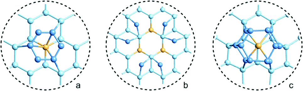 | ||
Fig. 1 Schematic representations of (a) a  ring cluster (b) a ring cluster (b) a  ring cluster and (c) a surface-absorbed M@Si12 molecule. Metal atoms, surface silicon atoms and additional silicon atoms are shown as yellow, light blue and blue balls, respectively. ring cluster and (c) a surface-absorbed M@Si12 molecule. Metal atoms, surface silicon atoms and additional silicon atoms are shown as yellow, light blue and blue balls, respectively. | ||
Datta and co-workers have set out the inherent challenges of computing electron transport properties on silicon,12 the most obvious being that it is a band-gap semi-conductor and not a metal. The effects of charge depletion due to absorption of a molecule can also extend several layers into the surface of crystal, necessitating the use of a relatively deep surface unit cell. Moreover, the perfect silicon(111) surface (the most readily accessed surface from bulk cleavage) is highly reactive due to the presence of ‘dangling bonds’ on the unsaturated silicon atoms, and rapid reconstruction occurs under ambient conditions to form an Si(111)-(2 × 1) reconstructed surface where the dangling bonds arrange into π-bonded chains.13,14 Above 400 °C, a further more complex reconstruction occurs to generate the Si(111)-(7 × 7) surface featuring ad-atoms, dimeric units and deep ‘corner holes’.15–17 The dangling bonds on the Si(111) surface introduce a finite density of states in the band gap, the precise structure of which is highly dependent on the subtleties of the surface reconstruction (vide infra). The energy associated with absorption of small molecules can also be competitive with the intrinsic driving forces for reconstruction and, as a result, the process of absorption can change the nature of the reconstruction or even quench it entirely.18 A combination of all these challenges means that there have been relatively few studies of electron transport properties of molecules on silicon surfaces, although silicon clusters sandwiched between Au and Si electrodes have been reported by Seminario and Yan.19 The aim of this paper is to use theory to establish the degree to which the intrinsic electronic fingerprint of the cluster survives the process of surface absorption, and therefore the extent to which it is valid to interpret the measured STM properties in terms of the isolated molecule. To do so, we first explore the structural and energetic aspects of the absorption of M@Si12 clusters on the silicon surface, and then consider how the perturbation of the molecule by the surface and vice versa impacts on the transmission properties of the junction.
Computational methods
The properties of the isolated gas-phase molecule W@Si12 were calculated using the ADF software package (ADF2013.01)20 with the PBE functional.21 Polarised all-electron Slater-type basis sets of triple-ζ and double-ζ quality (TZP/DZP) were used for tungsten and silicon, respectively.22 Scalar relativistic effects were included according to the zeroth-order regular approximation (ZORA) to the Dirac equation in all calculations.23 The absorption of the molecule on a surface was probed using a plane-wave basis (280 eV cutoff) in VASP, version 5.3.2,24 with the PW91 functional and projector-augmented wave pseudopotentials.25 The Si(111)-(7 × 7) surface was modelled using two bilayers of the unreconstructed (111) surface, the unsaturated valences on the lower layer being passivated with hydrogens. This equates to a Si200H49 unit cell. In the ab plane, the hexagonal lattice parameters are a = b = 26.88 Å and a vacuum separation of 10 Å was left between the periodic repetitions along c. The Si atoms in the passivated layer were kept fixed at their bulk positions to avoid unphysical perturbations to the surface. A 2 × 2 × 1 Monkhorst–Pack k-point grid was used to sample the Brillouin zone for all cases based on the 7 × 7 reconstructed surface.26 For calculations based on the Haneman and Pandey reconstructions we used a 3-bilayer deep 4 × 4 expansion of the unit cell of the unreconstructed surface in the a and b directions. The unsaturated valences on the lower surfaces were again passivated with hydrogens, giving a Si96H16 unit cell. A 4 × 4 × 1 Monkhorst–Pack grid was used for calculations based on a 2 × 2 × 1 unit cell. The electron transport properties of the absorbed cluster were calculated using the Atomistix Tool Kit (ATK), version 2016.4,27 using the PBE functional and polarised numerical LCAO basis sets of double-ζ polarized on all atoms.28 The Brillouin zone is sampled on a 5 × 5 × 100 Monkhorst–Pack grid. The eigenstates of the molecular projected self-consistent Hamiltonian (MPSH) are computed to provide a direct connection to the eigenvalues of the Kohn–Sham Hamiltonian of the isolated molecule. The MPSH eigenstates were projected onto the cluster, the four gold tip atoms, the seven surface silicon atoms that are connected directly with the cluster and three further surrounding silicon atoms.Results and discussion
Electronic structure of the W@Si12 cluster
The electronic structure of D6h-symmetric hexagonal prismatic clusters such as Cr@Si12, Mo@Si12 and W@Si12 has been studied extensively by us8b and several other authors,7 so we offer only a brief summary of the most relevant features of the electronic structure here. The W–Si bonding is dominated by the eight electrons in degenerate orbitals with W dxz/yz and dx2−y2/xy character (2e1g and 2e2g, respectively, in Fig. 2). A feature of some relevance to the subsequent discussion of surface binding is the cluster LUMO, with dominant metal dz2 character, directed along the 6-fold axis of the cluster (5a1g in Fig. 2). The presence of the vacant but almost entirely non-bonding metal dz2 orbital renders this 16-electron cluster highly electron deficient, to the extent that the ground state of valence isoelectronic [Mn@Si12]+ is in fact a biradical where this orbital is singly occupied.29 In the context of surface binding, the vacant dz2 orbital provides a facile pathway for the formation of covalent bonds to the silicon surface. One final point of relevance to the discussion is the unsaturation of the Si–Si bonds that make up the Si12 framework. A completely saturated Si12 cluster would have 5n = 60 valence electrons, so the total electron count of only 54 in W@Si12 implies a degree of unsaturation. The vacant 3b2u and 3e2u orbitals shown in Fig. 2 have distinct Si–Si π* character: these orbitals will prove to play an important role in binding the cluster to the surface.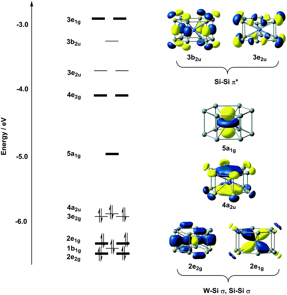 | ||
| Fig. 2 Kohn–Sham orbital array of the isolated W@Si12 cluster. | ||
Models of the reconstructed silicon surface
Low-index silicon surfaces are well known to undergo complex reconstructions, the study of which has relied heavily on the interpretation of low-energy-electron diffraction (LEED) data. The idealised surface, shown in Fig. 3b, has local 3-fold symmetry, but even at temperatures as low as 9 K a rapid reconstruction is observed.30 The earliest atomic-scale model for the Si(111) surface was due to Haneman (Fig. 3c), where alternate atoms in the surface layer are raised.31,32 Based on polarisation-dependent angle-resolved photoemission spectroscopy (ARUPS) experiments,33,34 Pandey proposed an alternative 2 × 1 model where the adatoms form zigzag π-bonded chains (Fig. 3d).14 Northrup and Cohen's calculations show that Pandey's model is the more stable of the two and, moreover, that it can be accessed easily from the perfect (111) surface via a barrier of only 0.03 eV per surface atom.35 STM images of the 2 × 1 reconstructed (111) surface confirm the presence of the parallel rows of atoms in Pandey's model.36,37 When the 2 × 1 reconstructed (111) surfaces are annealed at elevated temperatures, a further, irreversible, rearrangement occurs to a more complex 7 × 7 reconstruction described by Takayanagi's “dimer-adatom-stacking fault” (DAS) model, shown in Fig. 3a.17,38 The Si(111)-(7 × 7) unit cell is divided into “faulted” and “unfaulted” halves, each of which has six surface adatoms along with deep holes at the corners that penetrate to the base layer. There are 19 unsaturated valences (i.e. 3-coordinate Si atoms) in the 7 × 7 unit cell: twelve on adatoms (dark blue in Fig. 3a), six on atoms in the ‘rest’ layer (green) and, finally, one per unit cell at the base of the deep corner hole (red). Moreover, in each half of the unit cell the six adatoms separate into two symmetry-distinct types: three at the corners, in the vicinity of the deep surface holes (identified in Fig. 3(a) by the red circles at A and A′), and three in the centre of the unit cell (B and B′). The reduction in the number of dangling valences from 49 in an unreconstructed 7 × 7 expansion of the (111) surface unit cell to 19 in the DAS model provides the driving force for the reconstruction, and early DFT calculations by Brommer et al.39 confirmed its stability relative to Pandey's 2 × 1 reconstruction.14 This thermodynamic stability has made Si(111)-(7 × 7) the surface of choice for many studies of surface absorption, including the work by Kanayama and co-workers that is the motivation for our work.9 We begin our study of cluster absorption by considering the large 7 × 7 reconstructed DAS model but, ultimately, a unit cell of these dimensions is impractical for the subsequent study of transmission, where a large number of sub-surface layers are required. We therefore also consider the smaller reconstructions of Haneman and Pandey which are more amenable to transport calculations, with the aim of establishing the extent to which the important features of surface absorption identified on the Si(111)-(7 × 7) surface can be reproduced satisfactorily using smaller models.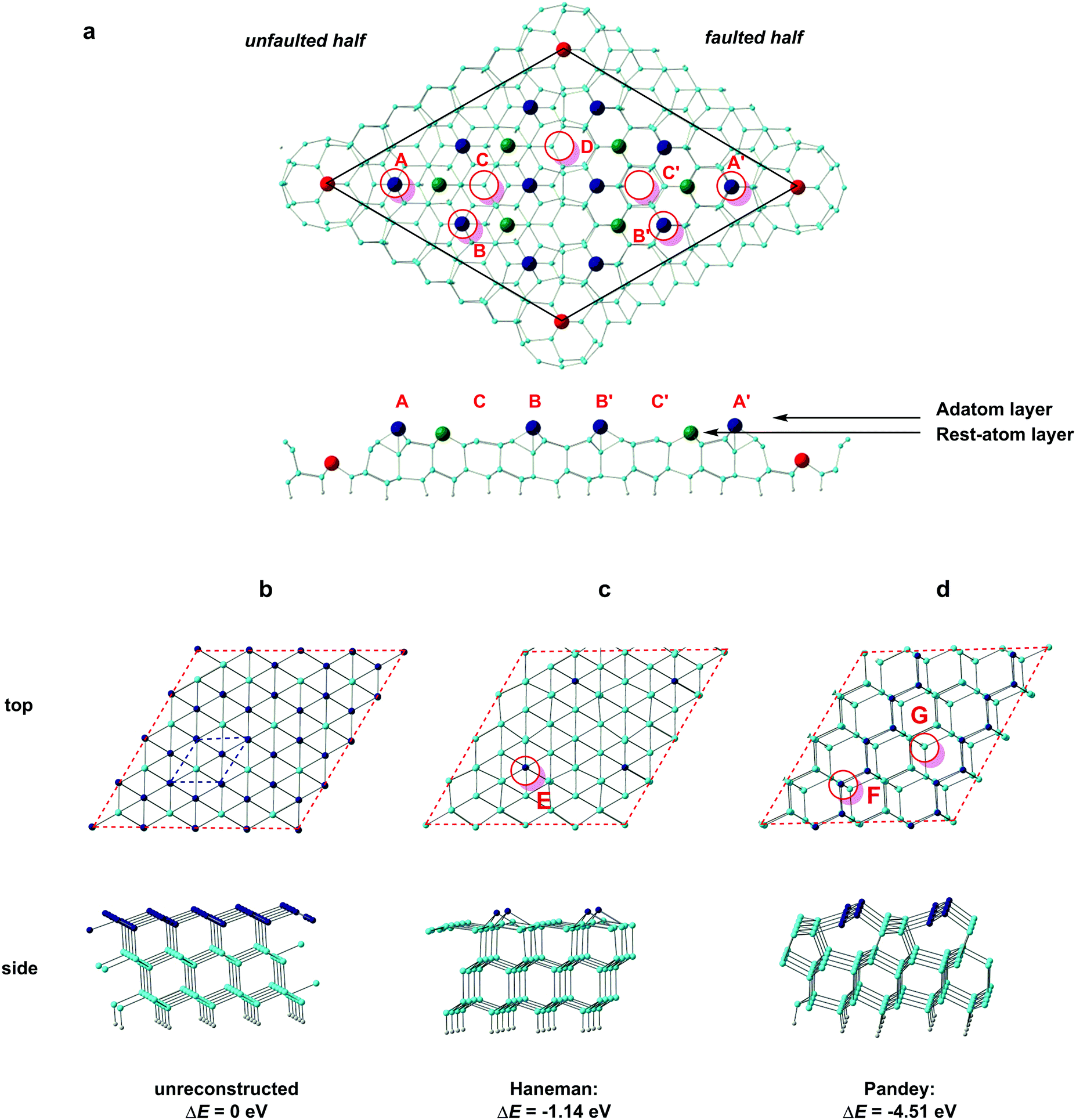 | ||
| Fig. 3 Models of silicon surfaces (red circles mark possible sites for absorption of a W@Si12 cluster): (a) the “DAS” model of the 7 × 7 reconstructed surface, (b) an unreconstructed Si(111) surface, (c) Haneman's 2 × 2 reconstruction and (d) Pandey's 2 × 1 zigzag chain model. The blue dashed line in (b) indicates the intrinsic 1 × 1 unit cell of the (111) surface while red dashed lines indicate the unit cells used in the calculations (7 × 7 expansion and 4 × 4 expansions in a and b, c, d, respectively). | ||
Absorption of the W@Si12 cluster on Si(111)-(7 × 7)
A number of previous authors have considered the site preferences for absorption of atoms or small molecules on Si(111)-(7 × 7). Early work by Brommer and co-workers used the concept of local softness to predict the preference for corner holes, adatoms and rest atoms as a function of the properties of the adsorbate (electron donor or acceptor).40 More recently, STM studies on hydrogen absorption have indicated a clear preference for absorption on top of either ‘rest’ atoms or surface adatoms41 while the group 11 metals Cu, Ag, Au, in contrast, bind preferentially to higher-coordinate sites on the surface.42 The different behaviour of the metals most likely reflects their larger size, which allows them to saturate the valence of three dangling bonds rather than only one. Even with monoatomic species, then, the landscape for absorption on the Si(111)-7 × 7 surface is a complex one. Rather fewer studies have been devoted to the absorption of molecular species, although Klamroth, Palmer and co-workers have reported a recent study of chemi- and physisorption of chlorobenzene on the 7 × 7 surface,43 where previous STM studies by Chen et al. had indicated a preference for absorption at the centre adatom of the faulted half.44 The authors constructed cluster models by slicing out fragments of the unit cell, and identified favourable chemisorption sites in the vicinity of the centre adatoms. We also note in this context the previous work of Robles and Khanna, who explored the absorption of Cr@Si12 on a perfect Si(111) surface. Although this model does not address the subtleties of the different absorption sites on the Si(111)-(7 × 7) surface, it highlights the potential importance of bond formation between the surface and both Cr and Si atoms of the cluster.45 Our calculations on the Si(111)-(7 × 7) surface employ a slab model with two layers of the unreconstructed lattice. The optimised structure of the clean surface (Fig. 3a) is very similar to that proposed by Takayanagi and computed by Brommer et al.,17,39 with prominent adatoms on both the faulted and unfaulted halves. The W@Si12 cluster was then docked onto several positions in the unit cell and the structure then relaxed to a local minimum. Specifically, we have considered docking onto each of the four symmetry-distinct adatoms shown in Fig. 3 (A, A′, B and B′) and also at C and C′ which have local 3-fold symmetry and are surrounded by three centre adatoms and three rest atoms, all with dangling valences. Finally, we have aligned the W@Si12 unit along the interface between the faulted and unfaulted halves of the unit cell via a hexagonal or a rectangular face (D and Dr, respectively). The structures and relative energies of the four most stable optimised structures (A, A′, C and C′) are summarised in Fig. 4 – the remaining four (A, A′, D and Dr) are shown in ESI,† Fig. S1. The most favourable absorption sites prove to be above the central adatoms (B or B′ on the unfaulted and faulted halves of the unit cell, respectively), and the relaxed geometry is locally very similar in both cases. The most conspicuous feature of the absorbed cluster is the formation of a direct bond between the W atom and the surface adatom (shown in dark blue in Fig. 4), at a distance of ∼2.6 Å in each case. The bonds between this adatom and two of the silicons in the rest-atom layer to which it was originally bonded are broken as a result, and these two silicons form covalent bonds to two atoms in the base hexagon of the cluster. Finally, two new Si–Si bonds are formed between the cluster and two of the unsaturated atoms in the rest layer (green). The bottom hexagon is split into two Si3 units, with a distinct hinging pushing three of the atoms in the upper hexagon upwards relative to the other three. The uppermost Si atoms of the cluster lie between 4.1 Å and 4.6 Å above the surface layer, a value that is consistent with Kanayama's upper limit of 4.4 Å for the surface features observed in the STM images.9 The energies of the B and B′ adducts are very close (ΔE = 0.06 eV) but the marginal preference for binding on the faulted half of the unit cell is at least consistent with the STM observations, where the ratio of clusters in the faulted and unfaulted halves was approximately 2![[thin space (1/6-em)]](https://www.rsc.org/images/entities/char_2009.gif) :1.9
:1.9
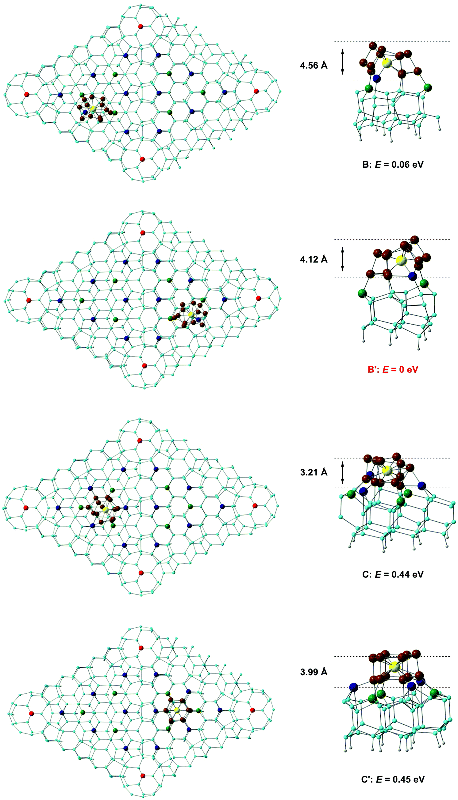 | ||
| Fig. 4 Structures and relative energies of W@Si12 clusters absorbed on the Si(111)-(7 × 7) surface. Positions B, B′, C and C′ are marked by red circles in Fig. 3. | ||
The structures of the A and A′ isomers, where the cluster binds to a corner adatom rather than a central one, are qualitatively very similar to B and B′, but are ∼0.8 eV higher in energy (ESI,† Fig. S1). A short surface Si–W bond is again present in both cases, as is the distinct puckering of the upper Si6 hexagonal layer: this feature therefore appears to be characteristic of bonding to a surface adatom. Several explanations for the general preference for adsorption at the centre rather than corner adatoms have been put forward in the literature, including the possibility that it relates to the presence of two strained dimer units in the proximity of the corner adatom but only one for the centre.46 In the case of the rather large W@Si12 substrate, however, there is a rather simpler explanation. When the surface Si–W bond is formed at a corner adatom (A, A′), there is only a single unsaturated rest-layer atom (green in Fig. 3a) available to form a bond to the base hexagon of the cluster whereas there were two for the centre adatoms (B and B′).
When the cluster docks at C or C′, we find that six new Si–Si bonds are formed to the basal hexagon of the cluster, three from the surrounding centre adatoms (blue) and three from the unsaturated atoms in the rest layer. We recall that in the Kohn–Sham orbital diagram of W@Si12 (Fig. 2) there are precisely three vacant Si–Si π* orbitals (3b2u and 3e2u) so the formation of six new Si–Si bonds saturates the cage. The W atom, however, remains 12-coordinate, with no evidence for formation of a new surface Si–W bond. The cluster unit also retains approximate 3-fold symmetry to a far greater extent than in any of A, A′, B or B′, and its hexagonal prismatic parentage is more obvious, particularly in C′. Both C and C′ are, however, ∼0.5 eV less stable than either B or B′. The cluster also remains recognisably hexagonal prismatic in both D and Dr, where the cluster binds to the junction between the faulted and unfaulted halves, but the energies are 1.61 and 3.84 eV higher than B′, respectively, suggesting that the faulted/unfaulted junction is unlikely to densely populated with clusters. In summary, our survey of the potential energy surface for binding to the Si(111)-(7 × 7) surface has revealed two quite distinct modes of binding. In the first (A, A′, B, B′) a surface adatom forms a direct covalent bond to the W atom, while three (A, A′) or four (B, B′) atoms from the rest-atom layer bond to the lower hexagon of the cluster. In C and C′, in contrast, there is no surface Si–W bond but six dangling valences on the surface form six new Si–Si bonds between the surface and the cluster. The calculations suggests that the W–Si surface bond confers greater stability in this case, but in general the balance between M–Si and Si–Si bonding is likely to be sensitive to the identity of the metal as well as the choice of computational methodology.
Absorption of the W@Si12 cluster on Si(111)-(2 × 1) surfaces
We have alluded above to the fact that the 7 × 7 unit cell is too large for the calculation of transmission properties, simply because the unit cells also need to be several layers deep in order to buffer any charge accumulation at the surface. We have therefore turned to the smaller reconstructions proposed by Haneman and Pandey, where the reduced surface area allows for greater depth in the unit cells (we have used three Si layers rather than two in the Si(111)-(7 × 7) model). Models for the Haneman and Pandey reconstructions are shown in Fig. 3(c) and (d), and, in the absence of substrate, lie 1.14 eV and 4.51 eV below the unreconstructed Si(111) surface, respectively (relative energies are given per unit cell). The clear preference for Pandey's zigzag chain model is consistent with experiment36 and also with Northrup and Cohen's previous calculations.35 For absorption of the W@Si12 unit on the Haneman and Pandey models, we have initialised calculations at three distinct sites E, F and G in Fig. 3c and d, leading to the corresponding minima shown at the top of Fig. 5. The most stable surface geometry, E, is obtained starting from Haneman's reconstruction: the equilibrium geometry features a surface Si–W bond at ∼2.6 Å similar to that identified in the B and B′ isomers on the 7 × 7 surface (Fig. 4), and the cluster unit is also substantially distorted from its original hexagonal prismatic form. The geometry of E is also very similar to that reported by Robles and Khanna for Cr@Si12 on an unreconstructed Si(111) surface.45 In contrast, the most stable geometry obtained starting from the Pandey surface, structure F in Fig. 5, does retain the zigzag structural signature of the original reconstruction, along with the characteristic W–Si surface bond of ∼2.6 Å. This difference reflects the intrinsically greater driving force for the Pandey reconstruction (4.51 eV vs. 1.14 eV), which will more effectively resist perturbation by the molecule on the surface. The fact that E, where the surface reconstruction is minimal, is 1.26 eV more stable than F (where it remains very prominent) is a clear indication of the very strong chemisorption of W@Si12 in the former. The antagonism between surface binding and surface reconstruction has been emphasised previously by Illas and co-workers in their work on group II metal adatoms on Si(111) and Ge(111) surfaces, where the energetic effect of substrate binding exceed that of reconstruction.18 In this case the tension is probably compounded by the local symmetries of the surface and substrate: the Pandey reconstruction removes the local 3-fold rotation symmetry about each surface adatom, making the surface less compatible with an intrinsically 6-fold symmetric substrate. In Pandey's zigzag π chain model the cluster is forced to bind in a ‘4 + 2’ mode, bridging two parallel chains, and must therefore distort substantially to bridge the gap between the chains. The local 3-fold rotational symmetry about each surface atom in the unreconstructed surface is somehow intrinsically more compatible with the hexagonal prismatic substrate. Neither of the 2 × 1 models presents a surface site precisely analogous to the C/C′ sites of the Si(111)-(7 × 7) model, where the cluster is surrounded by three adatoms and three unsaturated atoms of the rest layer. However, optimisation stating from position G on the Pandey reconstructed surface (Fig. 3e) generates the third structure shown in Fig. 5, where at least there is no surface W–Si bond. This structure is substantially less stable than the other two (+2.80 eV relative to E), but it provides the most direct model of the 7 × 7 sites C and C′ available within the constraints of the smaller unit cell. Finally, we have also considered the possibility that the cluster ‘hard lands’ on the surface, creating a partial monolayer of twelve additional silicon atoms on the surface. All such structures are ∼1 eV higher in energy than E (two examples, I and II, are shown in ESI,† Fig. S2). In summary, it seems that the more computationally tractable 2 × 1 reconstructed surfaces reproduce most, but not all, of the important features observed in the 7 × 7 alternative. We therefore proceed with a detailed analysis of the electronic structure and transmission properties of the model systems E. F and G on the basis that they capture at least the critical features of surface bonding in the Si(111)-(7 × 7) surface used in the experiments. The Density of States (DOS) projected onto the W 5d orbitals is also shown for the three structures of interest, E, F and G, in Fig. 5. The Kohn–Sham orbitals for the isolated W@Si12 cluster shown in Fig. 2 are included again as a point of reference.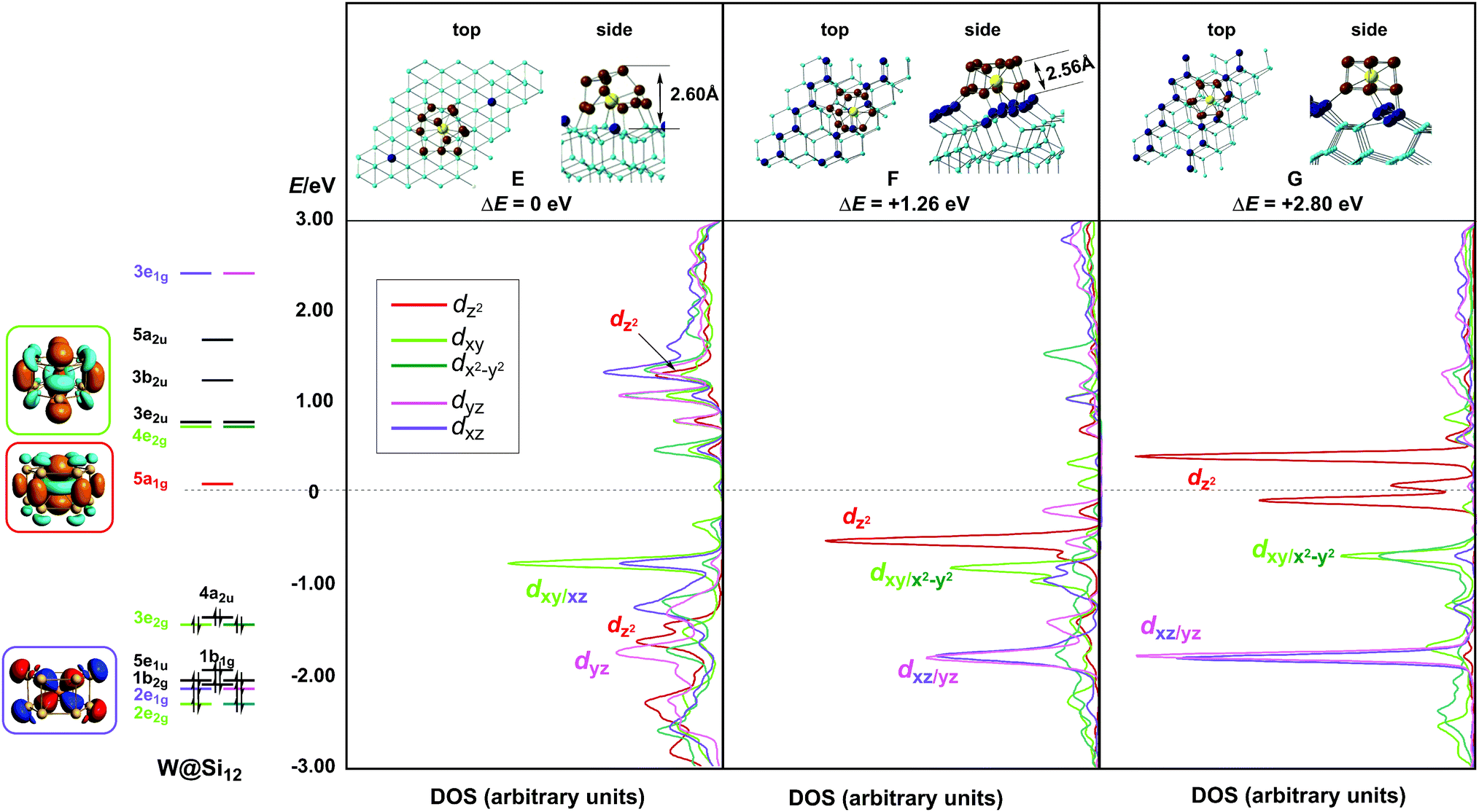 | ||
| Fig. 5 Optimised structures of W@Si12 clusters absorbed at sites E, F and G of Fig. 3, and the associated DOS projected onto the W 5d orbitals. The Kohn–Sham orbitals of W@Si12 are included for reference. | ||
Although not the most stable adduct, structure F affords the most direct comparison with the isolated cluster because the 3-fold rotational symmetry is, to a very good approximation, retained and the principal axis lies approximately normal to surface. Compared to the isolated cluster, the most significant feature of the DOS of F is the prominent W dz2 band ∼0.5 eV below the Fermi level (shown in red), with a smaller more dispersed dz2 component in the virtual manifold. Recall that the orbital with dominant W dz2 character (5a1g) is vacant in the isolated cluster, so the appearance of W dz2 character in the occupied manifold is a clear electronic signature of the formation of the bond between the W centre and the surface silicon atom (W–Si ∼2.6 Å). The surface binding can be viewed as a donor–acceptor interaction, where the LUMO of the isolated cluster acts as an effective acceptor of electron density through the formation of a W–Si bond. This stabilisation of the dz2 band upon binding to the surface may also be responsible for the emergence of a magnetic moment in Robles and Khanna's study of Cr@Si12, where single rather than double occupation of the 3d orbitals will be favoured due to punitive 3d–3d repulsions.45 The dxz/yz and dx2−y2/xy bands remain almost degenerate and at similar energy to the 2e1g and 3e2g orbitals of the parent cluster, respectively, consistent with the near-perfect 3-fold rotational symmetry of the absorbed cluster. The DOS of F is therefore immediately recognisable as that of a W@Si12 molecule, despite the formation of strong covalent W–Si and Si–Si bonds between the molecule and the surface. Similar observations can be made about the DOS of structure G, where the cluster also retains its hexagonal prismatic shape. The important difference here is that there is no W–Si surface bond, and as a result the W dz2 band (red) remains largely above the Fermi level, as it was in the isolated molecule. Otherwise, the positions and degeneracies of the dxz/yz and dx2−y2/xy bands again reflect the relatively unperturbed nature of the cluster unit. Structure E, in contrast, is the most distorted of the three and the axis of quantisation (the surface normal) does not coincide with any surviving rotational axis of the cluster unit. As a result the mapping onto individual angular momentum components is less helpful and the relationship to the orbitals of the isolated cluster less obvious. Nevertheless, it clear that the general features of the DOS are rather similar to those of F: in particular, the DOS at the Fermi level is negligible and a prominent band with W d character (in this case dxy/yz) appears at ∼−0.7 eV.
Electron transport through the cluster/surface junction
Finally, in order to establish the link to the STM images reported by Kanayama,9 we have computed the energy-dependent transmission spectrum, T(E), which in turn is related to the current flow between the surface and the STM tip. We note here that the STM experiments were performed with a negative sample bias (−2.5 V), so it is the region below the Fermi level that is most relevant in terms of the comparison to experiment. Our model of the surface/tip interface, shown in Fig. 6, includes two electrodes, one made of bulk silicon and the other bulk gold. The W@Si12 cluster is bound to the silicon surface in geometries E, F and G, while the STM tip is modelled by a pyramid of four gold atoms protruding from the Au(111) surface (Fig. 6a). In our device model we choose to place the tip 4.15 Å vertically above the highest lying silicon atom on the cluster surface (i.e. more than the sum of the covalent radii). This choice is justified more fully in the ESI,† Fig. S3. The zero-bias transmission spectra for structures E, F and G are shown as the black, red and green traces, respectively, in Fig. 6b, along with isosurfaces of the eigenstates of the molecular projected self-consistent Hamiltonian (MPSH) that dominate the transmission at each peak. The transmission spectrum of F (red trace) shows a prominent peak (peak 1) at ∼−0.6 eV coincident with the W dz2 band in the DOS in Fig. 5, and a second rather less intense feature (peak 2) at −1.8 eV, coincident with the dxz/yz band in the DOS. The MPSH isosurfaces confirm that the transmission peaks have a similar origin: peaks 1 and 2 clearly have dz2 and dxz character, respectively. The corresponding spectrum for the most stable structure, E (black trace), is qualitatively similar with a peak at −0.8 eV, almost coincident with the first major band below the Fermi level in the corresponding DOS plot. The projection onto specific angular momentum components is again less informative because of the low symmetry of the absorbed cluster but the iso-surface shown for peak 1 confirms the qualitative similarity to peak 2 of F. The relative intensities of peaks 1 and 2 in the two structures correlate with the extent to which the relevant orbitals are involved in the W–Si surface bond. In both E and F, the more intense of the two peaks (peak 2 for E, peak 1 for F) corresponds to the orbital aligned along the surface Si–W bond. On this basis, it seems that it is the W–Si surface bond that provides the most important pathway for tunnelling from the bulk silicon into the gold tip. The transmission spectrum of G (green trace), where a W–Si surface bond is conspicuously absent, supports this argument: the spectrum is entirely devoid of intense features between the Fermi level and −1.9 eV, and there is no transmission peak in the energy window coincident with the dz2 band in the DOS. In the absence of a direct covalent bond between the surface and the tungsten atom, the dz2 channel is therefore effectively silent.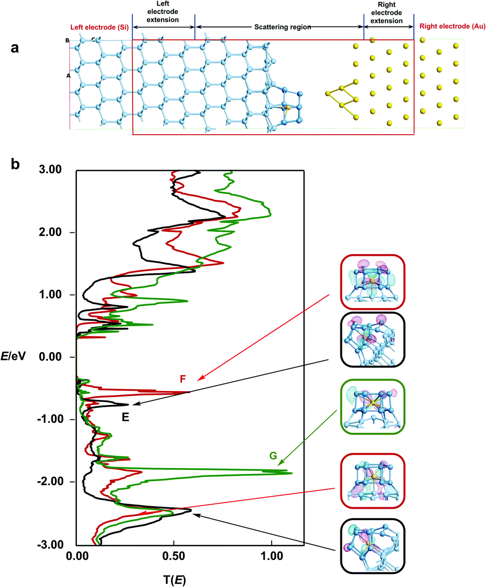 | ||
| Fig. 6 (a) Model scattering region used for the transmission calculations, (b) transmission spectra, T(E), for surface models E (black trace), F (red trace) and G (green trace). | ||
Conclusions
In this paper, we have traced the electronic fingerprint of the endohedral silicon cluster, W@Si12, through the DOS of its surface-bound states, all the way through to the computed transmission spectrum, providing a direct link to the scanning tunnelling microscopy experiment. The picture that emerges is that the W 5dz2 orbital, the LUMO of the isolated cluster, plays a central role in anchoring the cluster to the silicon surface through the formation of a thirteenth W–Si bond. The W–Si σ bonding orbital then provides an efficient transmission channel that allows current to flow from the silicon bulk into the tip of the gold electrode at moderate bias. The propensity of the W@Si12 cluster to form an additional W–Si surface bond is probably connected to the fact that in Beck's experiments, clusters with the M@Si12 stoichiometry react with additional Si atoms to generate larger clusters, M@Si14/15/16. The Si(111)-7 × 7 surface, with its under-coordinated silicon adatoms, can be regarded in this context as a nascent source of Si atoms. In alternative binding geometries where the cluster is bound to the surface exclusively through Si–Si bonds, transmission is much less intense out to almost 2 eV. Based on this analysis, we believe that the STM experiment provides a window not just into the structure of the cluster, but also into the nature of the bonding that stabilises it on the surface.Conflicts of interest
There are no conflicts to declare.Acknowledgements
The authors acknowledge financial support from the Engineering and Physical Sciences Research Council (EPSRC UK), grant number EP/K021435/1.Notes and references
- H. Häkkinen, Nat. Chem., 2012, 4, 443–455 CrossRef.
- S. M. Beck, J. Chem. Phys., 1987, 87, 4233–4234 CrossRef CAS.
- S. M. Beck, J. Chem. Phys., 1989, 90, 6306–6312 CrossRef CAS.
- (a) E. Janssens, P. Gruene, G. Meijer, L. Wöste, P. Lievens and A. Fielicke, Phys. Rev. Lett., 2007, 99, 063401 CrossRef PubMed; (b) P. Claes, E. Janssens, V. T. Ngan, P. Gruene, J. T. Lyon, D. J. Harding, A. Fielicke, M. T. Nguyen and P. Lievens, Phys. Rev. Lett., 2011, 107, 173401 CrossRef CAS PubMed; (c) V. T. Ngan, E. Janssens, P. Claes, J. T. Lyon, A. Fielicke, M. T. Nguyen and P. Lievens, Chem. – Eur. J., 2012, 18, 15788–15793 CrossRef CAS PubMed; (d) W.-J. Zheng, J. M. Nilles, D. Radisic and K. H. Bowen, Jr., J. Chem. Phys., 2005, 122, 071101 CrossRef PubMed; (e) J. T. Lau, K. Hirsch, P. Klar, A. Langenberg, F. Lofink, R. Richter, J. Rittmann, M. Vogel, V. Zamudio-Bayer, T. Möller and B. v. Issendorff, Phys. Rev. A: At., Mol., Opt. Phys., 2009, 79, 053201 CrossRef; (f) J. T. Lau, M. Vogel, A. Langenberg, K. Hirsch, J. Rittmann, V. Zamudio-Bayer, T. Möller and B. von Issendorff, J. Chem. Phys., 2011, 134, 041102 CrossRef CAS.
- H. Hiura, T. Miyazaki and T. Kanayama, Phys. Rev. Lett., 2001, 86, 1733–1736 CrossRef CAS.
- (a) M. B. Abreu, A. C. Reber and S. N. Khanna, J. Chem. Phys., 2015, 143, 074310 CrossRef PubMed; (b) J. Lu and S. Nagase, Phys. Rev. Lett., 2003, 90, 115506 CrossRef.
- (a) J.-G. Han, C.-Y. Xiao and F. Hagelberg, Struct. Chem., 2002, 13, 173–191 CrossRef CAS; (b) S. N. Khanna, B. K. Rao and P. Jena, Phys. Rev. Lett., 2002, 89, 016803 CrossRef CAS; (c) F. Hagelberg, C. Xiao and W. A. Lester, Jr., Phys. Rev. B: Condens. Matter Mater. Phys., 2003, 67, 035426 CrossRef; (d) V. Zamudio-Bayer, L. Leppert, K. Hirsch, A. Langenberg, J. Rittmann, M. Kossick, M. Vogel, R. Richter, A. Terasaki, T. Möller, B. v. Issendorff, S. Kümmel and J. T. Lau, Phys. Rev. B: Condens. Matter Mater. Phys., 2013, 88, 115425 CrossRef; (e) Z.-H. Sun, H. Oyanagi, N. Uchida, T. Miyazaki and T. Kanayama, J. Phys. D: Appl. Phys., 2009, 42, 015412 CrossRef.
- (a) X. Jin, V. Arcisauskaite and J. E. McGrady, Dalton Trans., 2017, 46, 11636–11644 RSC; (b) J. M. Goicoechea and J. E. McGrady, Dalton Trans., 2015, 44, 6755–6766 RSC; (c) X. Jin, V. Arcisauskaite and J. E. McGrady, Adv. Inorg. Chem., 2019, 73, 265–304 CrossRef.
- N. Uchida, L. Bolotov, T. Miyazaki and T. Kanayama, J. Phys. D: Appl. Phys., 2003, 36, L43–L46 CrossRef CAS.
- (a) N. Uchida, H. Yahata, T. Kanayama and L. Bolotov, Appl. Phys. Lett., 2007, 91, 06319 Search PubMed; (b) R. J. Wilson and S. Chiang, Phys. Rev. Lett., 1987, 58, 369–372 CrossRef CAS PubMed; (c) P. A. Bennett, M. Copel, D. Cahill, J. Falta and R. M. Tromp, Phys. Rev. Lett., 1992, 69, 1224–1227 CrossRef CAS PubMed; (d) M.-H. Tsai, J. D. Dow, P. A. Bennett and D. G. Cahill, Phys. Rev. B: Condens. Matter Mater. Phys., 1993, 48, 2486–2492 CrossRef.
- J.-Y. Cheng, B. L. Fisher, N. P. Guisinger and C. M. Lilley, npj Quantum Mater., 2017, 2, 25 CrossRef.
- T. Rakshit, G.-C. Liang, A. W. Ghosh and S. Datta, Nano Lett., 2004, 4, 1803–1807 CrossRef CAS.
- R. E. Schlier and H. E. Farnsworth, J. Chem. Phys., 1959, 30, 917–926 CrossRef CAS.
- K. C. Pandey, Phys. Rev. Lett., 1981, 47, 1913–1917 CrossRef CAS.
- J. J. Lander, G. W. Gobeli and J. Morrison, J. Appl. Phys., 1963, 34, 2298–2306 CrossRef CAS.
- R. M. Feenstra and M. A. Lutz, Surf. Sci., 1991, 243, 151–165 CrossRef CAS.
- K. Takayanagi, Y. Tanishiro, M. Takahashi and S. Takahashi, J. Vac. Sci. Technol., A, 1985, 3, 1502–1506 CrossRef CAS.
- J. M. Ricart, J. Rubio and F. Illas, Phys. Rev. B: Condens. Matter Mater. Phys., 1990, 42, 5212–5220 CrossRef CAS.
- L. Yan and J. M. Seminario, Int. J. Quantum Chem., 2007, 107, 440–450 CrossRef CAS.
- (a) G. te Velde, F. M. Bickelhaupt, E. J. Baerends, C. Fonseca Guerra, S. J. A. van Gisbergen, J. G. Snijders and T. Ziegler, J. Comput. Chem., 2001, 22, 931–967 CrossRef CAS; (b) C. Fonseca Guerra, J. G. Snijders, G. te Velde and E. J. Baerends, Theor. Chem. Acc., 1998, 99, 391–403 Search PubMed; (c) E. J. Baerends, T. Ziegler and A. J. Atkins, ADF 2013, SCM, Theoretical Chemistry, Vrije Universiteit, Amsterdam, The Netherlands, https://www.scm.com Search PubMed.
- J. P. Perdew, K. Burke and M. Ernzerhof, Phys. Rev. Lett., 1996, 77, 3865–3868 CrossRef CAS PubMed.
- E. van Lenthe and E. J. Baerends, J. Comput. Chem., 2002, 24, 1142–1156 CrossRef PubMed.
- (a) E. van Lenthe, E. J. Baerends and J. G. Snijders, J. Chem. Phys., 1993, 99, 4597–4610 CrossRef CAS; (b) E. van Lenthe, E. J. Baerends and J. G. Snijders, J. Chem. Phys., 1994, 101, 9783–9792 CrossRef CAS; (c) E. van Lenthe, R. van Leeuwen, E. J. Baerends and J. G. Snijders, Int. J. Quantum Chem., 1994, 57, 281–293 CrossRef; (d) E. van Lenthe, J. G. Snijders and E. J. Baerends, J. Chem. Phys., 1996, 105, 6505–6516 CrossRef CAS; (e) E. van Lenthe, A. Ehlers and E. J. Baerends, J. Chem. Phys., 1999, 110, 8943–8953 CrossRef CAS.
- (a) G. Kresse and J. Furthmüller, Phys. Rev. B: Condens. Matter Mater. Phys., 1996, 54, 11169–11186 CrossRef CAS; (b) G. Kresse and D. Joubert, Phys. Rev. B: Condens. Matter Mater. Phys., 1999, 59, 1758–1775 CrossRef CAS.
- (a) J. P. Perdew and W. Yue, Phys. Rev. B: Condens. Matter Mater. Phys., 1986, 33, 8800–8802 CrossRef; (b) J. P. Perdew and Y. Wang, Phys. Rev. B: Condens. Matter Mater. Phys., 1992, 45, 13244–13249 CrossRef.
- H. J. Monkhorst and J. D. Pack, Phys. Rev. B: Solid State, 1976, 13, 5188–5192 CrossRef.
- (a) M. Brandbyge, J.-L. Mozos, P. Ordejón, J. Taylor and K. Stokbro, Phys. Rev. B: Condens. Matter Mater. Phys., 2002, 65, 165401 CrossRef; (b) D. Stradi, U. Martinez, A. Blom, M. Brandbyge and K. Stokbro, Phys. Rev. B, 2016, 93, 155302 CrossRef; (c) Atomistix Toolkit version 2016.4, Synopsys QuantumWise A/S, http://www.quantumwise.com.
- S. Smidstrup, D. Stradi, J. Wellendorff, P. A. Khomyakov, U. G. Vej-Hansen, M.-E. Lee, T. Ghosh, E. Jónsson, H. Jónsson and K. Stokbro, Phys. Rev. B, 2017, 96, 195309 CrossRef.
- V. Arcisauskaite, D. Fijan, M. Spivak, C. de Graaf and J. E. McGrady, Phys. Chem. Chem. Phys., 2016, 18, 24006–24014 RSC.
- V. Y. Aristov, I. E. Batov and V. A. Grazhulis, Surf. Sci., 1983, 132, 73–81 CrossRef CAS.
- D. Haneman, Phys. Rev., 1961, 121, 1093–1100 CrossRef CAS.
- D. Haneman, Adv. Phys., 1982, 31, 165–194 CrossRef CAS.
- F. Houzay, G. M. Guichar, R. Pinchaux and Y. Petroff, J. Vac. Sci. Technol., 1981, 18, 860–865 CrossRef CAS.
- R. I. G. Uhrberg, G. V. Hansson, J. M. Nicholls and S. A. Flodström, Phys. Rev. B: Condens. Matter Mater. Phys., 1981, 24, 4684–4691 CrossRef CAS.
- J. E. Northrup and M. L. Cohen, Phys. Rev. Lett., 1982, 49, 1349–1352 CrossRef CAS.
- R. M. Feenstra, W. A. Thompson and A. P. Fein, Phys. Rev. Lett., 1986, 56, 608–611 CrossRef CAS PubMed.
- R. M. Feenstra, J. A. Stroscio and A. P. Fein, Surf. Sci., 1987, 181, 295–306 CrossRef CAS.
- S. D. Solares, S. Dasgupta, P. A. Schultz, Y.-H. Kim, C. B. Musgrave and W. A. Goddard, III, Langmuir, 2005, 21, 12404 CrossRef CAS PubMed.
- K. D. Brommer, M. Needels, B. E. Larson and J. D. Joannapoulos, Phys. Rev. Lett., 1992, 68, 1355–1358 CrossRef CAS PubMed.
- K. D. Brommer, M. Galván, A. Dal Pino, Jr. and J. D. Joannaopoulos, Surf. Sci., 1994, 314, 57–70 CrossRef CAS.
- R.-L. Lo, I.-S. Hwang, M.-S. Ho and T. T. Tsong, Phys. Rev. Lett., 1998, 80, 5584 CrossRef CAS.
- C. Zhang, G. Chen., K. Wang, H. Yang, T. Su, C. T. Chan, M. M. T. Loy and X. Xiao, Phys. Rev. Lett., 2005, 94, 176104 CrossRef PubMed.
- M. Utecht, T. Pan, T. Klamroth and R. E. Palmer, J. Phys. Chem. A, 2014, 118, 6699–6704 CrossRef CAS PubMed.
- X. Chen, Q. Kong, J. C. Polyani, D. Rogers and S. So, Surf. Sci., 1995, 340, 224–230 CrossRef CAS.
- R. Robles and S. N. Khanna, Phys. Rev. B: Condens. Matter Mater. Phys., 2009, 80, 115414 CrossRef.
- P. Avouris, J. Phys. Chem., 1990, 94, 2246–2256 CrossRef CAS.
Footnote |
| † Electronic supplementary information (ESI) available: Cartesian coordinates and total energies of all optimized structures. See DOI: 10.1039/c9cp01841g |
| This journal is © the Owner Societies 2019 |