
Electronic structure of Al, Ga, In and Cu doped ZnO/Cu(111) bilayer films†
Ho Viet
Thang
 * and
Gianfranco
Pacchioni
* and
Gianfranco
Pacchioni
Departimento di Scienza dei Materiali, Università di Milano-Bicocca, via Cozzi 55, 20125 Milano, Italy. E-mail: hvthangbk@gmail.com
First published on 26th November 2018
Abstract
The effect of doping with group-III metals (Al, Ga and In) and Cu free standing and Cu(111) supported ZnO bilayer films has been investigated computationally by using the DFT+U method including dispersion contributions. The changes in the electronic properties of doped ZnO and ZnO/Cu(111) films have been tested by adsorbing CO probe molecules. The replacement of a lattice Zn ion in a free-standing ZnO bilayer by a group-III element generates an extra electron whose distribution depends on the dopant. In particular, while the excess electron is delocalized over the conduction band for Al or Ga doping, it is localized on the dopant in the case of In. The situation is different on the supported ZnO/Cu(111) film, where the extra electron is transferred to the underlying Cu support. While the CO adsorption energy at the doped sites in the ZnO bilayer is the same as in the ZnO/Cu(111) ultrathin films, CO exhibits a larger red-shift in the unsupported ZnO bilayer. The oxidation state of Cu replacing Zn in the unsupported ZnO films is 2+, Cu(3d9) state, while it is 1+, Cu(3d10) state, in the ZnO/Cu(111) supported films where a charge transfer from the supporting Cu metal to the Cu impurity occurs. Cu doping results in a stronger interaction with CO and a large red-shift of the CO stretching frequency. In this respect, Cu doping of ZnO/Cu(111) bilayer films could have interesting consequences in gas adsorption while doping with group-III elements does not lead to major changes of the adsorption properties when the free-standing ZnO films are compared to the supported ZnO/Cu(111) counterparts.
1. Introduction
Zinc oxide is a material that finds applications in various fields: energy storage, catalysis, dyes, transistors, solar cells, electronic devices, gas sensing, etc.1 This largely depends on the typical properties of ZnO, e.g. a direct band gap of 3.37 eV at room temperature, transparency in the visible light range, and a high exciton binding energy of 60 meV.2 Furthermore, ZnO is nontoxic, cheap and abundant.3 However, the pristine material has some limitations in particular applications that need high carrier concentration, especially in conducting materials, or optoelectronic applications. To improve its electronic properties in these applications, there are various methods including controlled strain, applying an external electric field, or doping.1,4,5 Among these procedures, doping is the most commonly used method. Depending on the desired application, different heteroatoms can be used to dope ZnO. The introduction of group (III) elements (B, Al, Ga and In)6–8 in ZnO leads to n-type conductivity, which makes these dopants quite interesting for transparent conductors used in panel displays or solar cells. On the other hand, the replacement of Zn(II) by group-I elements (Li,9 K10 and Na11) or the substitution of lattice oxygen by group-V elements (N, P and As)12 induces p-type conductivity which makes the material suitable for use in photo-detectors, gas sensors, and transistors. However, the use of p-type dopants is limited by the competing formation of interstitial doping.12 Co-doping, such as, Li–N,13 P–N,14etc., is also studied to obtain p-type materials.Cu doped ZnO is widely used and has shown a significant enhancement in photocatalytic activity,15 gas sensor ability,16–18 and electrical, magnetic and optical properties.19–22 This is due to the similar electronic structure and atomic size of Cu and Zn. However, the oxidation state of Cu doping is either 1+ or 2+,23–25 depending on the chemical structure of the host and synthetic conditions used. Identifying the properties of excess electrons and holes created by dopants in ZnO provides useful information for the design of materials with tailored properties.
The properties of doped ZnO have been extensively investigated at the level of bulk, nanoparticles, nanowires, nanobelts, and also ultrathin films.26–28 So far, previous studies have focused on doped, free-standing ZnO films29 and on ZnO films supported on glass substrates18,19,23 or on polycarbonate substrates.8,30 In these systems the support does not play a critical role, and probably does not influence the electronic properties of the doped ZnO film.
Beside free-standing ZnO films,31 graphitic-like ZnO thin films on different metals, Cu,32,33 Ag,34,35 and Au36,37 have been reported in the last decade. ZnO films form spontaneously on a Cu surface during the catalytic process of hydrogenation of CO or CO2 to methanol over Cu/ZnO catalysts.38,39 The electronic and structural properties of these materials have been elucidated both theoretically and experimentally. The ZnO thin film is bound to the metal surface mainly thanks to dispersion forces.40 A nonpolar, flat structure of ZnO films was observed on Ag(111) and Au(111), whereas a very small rumpling was found when the ZnO bilayer is deposited on Cu(111). This is different from bulk ZnO wurtzite which exhibits polar (0001) or (000![[1 with combining macron]](https://www.rsc.org/images/entities/char_0031_0304.gif) ) surfaces.41
) surfaces.41
The molecular adsorption or catalytic properties of metal-supported ZnO thin films are modified by the occurrence of a charge transfer from the underlying metal support to the adsorbed species (e.g. Au atoms, NO2 molecules, etc.).42 A consequence is that Au20 clusters, which are tetrahedral (3D) in the gas-phase, assume a flat, 2D structure when they are deposited on ZnO/Cu(111) films.43 Also the formation energy of oxygen vacancies at interface sites is significantly reduced in supported ZnO films.44
In this paper, we extend the study to the effects of doping supported or unsupported ZnO bilayer films with Al, Ga, In and Cu atoms. To this end, we considered the effect of substitutional doping with both n-type (Al, Ga and In) and p-type (Cu) dopants on the electronic and geometric structure of ZnO/Cu(111) films and the corresponding free-standing ZnO bilayer by using the DFT+U approach. So far, no experimental results have been reported on the doping of supported ZnO films. However, doping of thin oxide films can be achieved via diffusion from the support or during the phase of oxide film deposition,45,46 showing that it is possible to produce these kinds of materials.
2. Computational methods
Spin-polarized periodic density functional calculations were carried out by using the VASP code.47,48 The exchange–correlation term was treated within the generalized gradient approximation in the Perdew–Burke–Ernzerhof (PBE) formulation.49 Core electrons were described according to the projector augmented wave (PAW) method.50,51 The valence electrons explicitly treated are: Zn(4s, 3d), C(2s, 2p), O(2s, 2p), Al(3s, 3p), Ga(4s, 4p), In(5s, 5p) and Cu(4s, 3d). The self-interaction error present in the PBE method was partly corrected by using a DFT+U approach. We set up a Hubbard-U52,53 value of 4.7 eV for the Zn 3d state54 which reproduced the lattice parameters of ZnO wurtzite. In particular, our scheme yields for the lattice parameters a = b = 3.22 Å and c = 5.20 Å, values that are close to the experimental data a = b = 3.25 Å and c = 5.21 Å.55 The dispersion interaction was described by the D2′ scheme in which R0 and C6 parameters from the original Grimme's D2 method56 are modified as proposed in the literature.57 The atoms were relaxed until forces are less than 0.01 eV Å−1. A 2 × 2 × 1 k-point mesh was used for structure optimization while a 6 × 6 × 1 k-point mesh was used for density of states calculations. This is due to the fact that the higher k-point mesh relaxation does not differ from lower k-point mesh relaxation. Particularly, the calculations with the 6 × 6 × 1 k-point mesh show that the CO adsorption energy is only 0.003 eV stronger than that obtained with the 2 × 2 × 1 k-point mesh, while the CO stretching frequency is the same. The dipolar correction was also considered in all calculations.A (3 × 3) supercell for a free standing ZnO bilayer and a (3 × 3) ZnO bilayer deposited on a (4 × 4) supercell of four atomic layer Cu(111) were used in this study. The details are described in a previous study.40 Al, Ga, In and Cu replace a Zn lattice ion in the doped ZnO models. For the ZnO bilayer, only one Zn position was considered, while on ZnO/Cu(111) one can replace Zn on the top or at the interface layers. This corresponds to 5.5% dopant concentration in the ZnO film which is consistent with experimental observations.58–60
CO adsorption was used to probe the effect of doping on the electronic properties of ZnO and ZnO/Cu(111) films. The CO adsorption energy was calculated as the difference between the adsorption complex and the isolated species. The harmonic CO stretching frequencies were obtained by considering the vibrations of CO and its nearest neighboring atoms; no scaling factor was applied and only shifts with respect to free CO will be discussed. The effective charges were calculated by means of the Bader method.61–64
The rumpling of the ZnO bilayer film for a given layer, R(l) is calculated as follows:
3. Results and discussion
3.1 Properties of the M-doped (M = Al, Ga, In and Cu) free-standing ZnO bilayer
We first discuss the electronic properties of a pristine, free-standing, ZnO bilayer optimized starting from a slab of the wurtzite (0001) surface. It has been shown by experiment37 and theory40 that the bilayer film has a graphitic-like structure, where Zn and O ions form a hexagonal structure and are lying in same plane, Fig. 1a. This is different from the wurtzite (0001) surface, where O and Zn atoms reside on different planes with a separation distance of 0.86 Å. In the optimized graphitic-like ZnO bilayer, the average Zn–O bond length in the plane is 1.895 Å, and the O–Zn–O angle is 120°. The calculated band gap of the pristine ZnO bilayer is 2.07 eV, close to previous estimates based on the GGA+U method, 2.18 eV.65 The film exhibits no magnetization, Table 1. The band gap of the ZnO bilayer is larger than that of bulk wurtzite computed at the same level, 1.42 eV. Both values are considerably smaller than the bulk experimental gap of 3.37 eV, due to an underestimate of this quantity at the DFT+U level.66 When ZnII is replaced by group-III elements (Al, Ga and In), an extra electron is introduced in the doped ZnO film. The localization of this extra charge strongly depends on the nature of dopant, Table 1. The Bader charge analysis shows that, going from Al, to Ga, to In, the effective charge decreases from 2.43|e| to 1.61|e| to 0.85|e|, respectively. The charge redistribution due to group-III doping also results in different electronic structures. Since the ZnO films are perfect and defect-free, for Al- and Ga-doping the excess electron occupies the empty states, the Fermi level moves into the conduction band, and the system is described as a metal, see the density of states (DOS) in Fig. 1b and c. In reality, the excess electrons provided by Al and Ga dopants can be trapped at defect sites, vacancies, and grain boundaries, so that the material still exhibits a band gap.67 | ||
| Fig. 1 Side view (left), top view (middle) and DOS profile (right) of the (a) pristine ZnO bilayer, (b) Al-doped ZnO bilayer, (c) Ga-doped ZnO bilayer, (d) In-doped ZnO bilayer and (e) Cu-doped ZnO bilayer. Zn, O, Al, Ga, In and Cu are blue, red, light-blue, green, purple and orange spheres, respectively. Spin density (transparent yellow) is plotted with an isosurface of 0.005|e| Å−3. | ||
| System | E g (eV) | q(M) (|e|) | Mag. (μB) | R(M–O) (Å) | ∠O–M–O (deg) |
|---|---|---|---|---|---|
| ZnO bilayer | 2.07 | 0.00 | 1.895 | 120 | |
| Al:ZnO bilayer | Metal | 2.43 | 0.00 | 1.783 | 116 |
| Ga:ZnO bilayer | Metal | 1.61 | 0.00 | 1.886 | 117 |
| In:ZnO bilayer | 2.46 | 0.85 | 1.00 | 2.141 | 102 |
| Cu:ZnO bilayer | 2.00 | 0.94 | 1.00 | 1.878 | 116 |
For In-doped ZnO, the excess electron resides on the In ion, a result corroborated by the presence of a mid-gap 5s state, and by the spin density on the In ion, Fig. 1d. Moreover, the more or less delocalized nature determines the final magnetic moment: absent in Al- and Ga-doping, while a magnetic moment of 1 μB (Bohr magneton) is found for In-doped ZnO, Table 1. The magnetic moment of 1.00 μB indicates, together with the spin density plot, the localization of an unpaired electron on In, which means that the formal oxidation state of In is II+. However, the corresponding Bader charge, +0.85, is smaller, see Table 1.
Doping also has different effects on the structural parameters of the ZnO film. Al and Ga ions are located mostly in the same plane of the hexagonal ring of O and Zn atoms. The Al–O and Ga–O bond lengths are shortened from 1.895 Å in pristine ZnO to 1.783 Å and 1.886 Å, respectively, while In-dopants are lying above the ZnO film due to steric reasons, and the In–O bond, 2.141 Å, expands considerably, Fig. 1d. The O–Al–O and O–Ga–O bond angles, 116° and 117°, respectively, are slightly smaller than the O–Zn–O bond angle of 120° on the pristine ZnO bilayer film; the O–In–O bond angle becomes much smaller, 102°. The large difference in the bond length and bond angle of In-dopants compared to Al and Ga is due to the fact that the ionic radius of In3+ (0.80 Å) is larger than that of Zn2+ (0.74 Å), while Al3+ (0.54 Å) and Ga3+ (0.62 Å) have smaller ionic radii than Zn2+.
The oxidation state of a Cu ion replacing Zn in the unsupported ZnO bilayer is obviously 2+, Cu 3d.9 Indeed, a magnetic moment of 1 μB is found, Table 1, see also the DOS profile, Fig. 1e. The Cu(II) state in doped ZnO films has been observed from the XPS spectra of Cu 2p3/219 and is supported by GGA+U calculations.65 Cu doping leads to a very small decrease of the band gap, from 2.07 eV (ZnO) to 2.0 eV (Cu-doped ZnO), Table 1. This is in line with previous results from the literature.65 Since the ionic radius of Cu2+ (0.77 Å) is similar to that of Zn2+ (0.74 Å), there is only a small reduction of the Cu–O bond length (1.878 Å) and of the O–Cu–O bond angle (116°), Table 1, compared to the undoped ZnO bilayer.
3.2 Properties of M-doped (M = Al, Ga, In, and Cu) ZnO/Cu(111) films
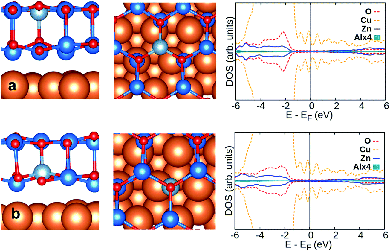
Firstly, we briefly describe the structural properties of pristine ZnO/Cu(111) films. The best fit of the graphitic-like ZnO bilayer film deposited on the Cu(111) surface consists of a (3 × 3) supercell of ZnO on a (4 × 4) supercell of Cu(111).40,68 There is a small expansion (2.3%) of the ZnO film, introducing some tensile strain, and a slight rumpling of 0.09 Å and 0.15 Å, respectively, for top and interface layers,40Table 2 and Fig. 2. This film binds to the metal surface mainly by dispersion forces, with a distance between the ZnO bottom layer and the Cu(111) support of about 2.5 Å. | ||
| Fig. 2 Side view (left) and top view (middle) of pristine ZnO/Cu(111) along with DOS profile (right). Zn, O and Cu are blue, red and orange spheres, respectively. | ||
Doping with group-III and Cu atoms of the supported ZnO/Cu(111) film has been considered by replacing Zn ions in two different positions, the top layer and the ZnO–Cu interface layer. Al and Ga prefer to replace Zn on the top layer, while for In and Cu doping is preferred at the interface between ZnO and Cu(111), Table 2. Compared to the free-standing ZnO bilayer, the effective charges in doped ZnO/Cu(111) are virtually the same for Al (+2.4|e|) and Ga (+1.6|e|). However, while in the ZnO bilayer the excess electron is delocalized over the conduction band, on ZnO/Cu(111) the extra electron is transferred to the Cu support, Fig. 3 and 4. This will become particularly clear when we will discuss CO adsorption, see below.
| System | ΔErel (eV) | ΔΦ (eV) | q(M) |e| | Mag. (μB) | d(ZnO–Cu) | R (Å) |
|---|---|---|---|---|---|---|
| Pristine ZnO/Cu(111) | 0.00 | 0.00 | 2.502/4.826 | 0.148/0.085 | ||
| Al:ZnO/Cu(111) | ||||||
| Surface | 0.00 | 0.11 | 2.42 | 0.00 | 2.589/4.893 | 0.151/0.086 |
| Interface | 0.45 | −0.05 | 2.46 | 0.00 | 2.600/4.893 | 0.120/0.084 |
| Ga:ZnO/Cu(111) | ||||||
| Surface | 0.00 | 0.27 | 1.60 | 0.00 | 2.601/4.947 | 0.274/0.115 |
| Interface | 0.31 | −0.05 | 1.50 | 0.00 | 2.582/4.894 | 0.033/0.086 |
| In:ZnO/Cu(111) | ||||||
| Surface | 0.41 | 0.23 | 1.46 | 0.00 | 2.574/4.962 | 0.172/0.146 |
| Interface | 0.00 | −0.09 | 1.29 | 0.00 | 2.600/4.943 | 0.180/0.103 |
| Cu:ZnO/Cu(111) | ||||||
| Surface | 0.58 | −0.15 | 0.72 | 0.00 | 2.521/4.835 | 0.150/0.070 |
| Interface | 0.00 | 0.02 | 0.66 | 0.00 | 2.543/4.897 | 0.173/0.100 |
 | ||
| Fig. 3 Side view (left) and top view (middle) of Al-doped ZnO/Cu(111) along with DOS profile (right): (a) Al doped on surface site and (b) Al doped in interface site. Zn, O, Cu and Al are blue, red, orange and light-blue spheres, respectively. | ||
 | ||
| Fig. 4 Side view (left) and top view (middle) of Ga-doped ZnO/Cu(111) along with DOS profile (right): (a) Ga doped on surface site and (b) Ga doped in interface site. Zn, O, Cu and Ga are blue, red, orange and green spheres, respectively. | ||
In the case of In, the charge on In is more positive on the supported film, by about +0.4|e| and +0.6|e| for top and interface sites, respectively, than on the free-standing ZnO film. This reflects the fact that the excess electron is transferred to the Cu support. This latter result is confirmed by the complete quenching of magnetic moment, Table 2, and by the absence of mid gap states, see the DOS profile, Fig. 5.
 | ||
| Fig. 5 Side view (left) and top view (middle) of In-doped ZnO/Cu(111) along with DOS profile (right): (a) In doped on surface site and (b) In doped in interface site. Zn, O, Cu and In are blue, red, orange and purple spheres, respectively. | ||
Opposite to In-doped ZnO/Cu(111), Cu-doped ZnO/Cu(111) shows a decrease of the Bader charge on the dopant compared to the free-standing ZnO bilayer, by about 0.22|e| and 0.28|e| for the top and interface layer doping, respectively, Tables 1 and 2. A smaller Bader charge on Cu-doped ZnO/Cu(111) is accompanied by a quenching of the magnetic moment, Table 2 and Fig. 6, due to a charge transfer from the underlying support to the Cu dopant that changes its oxidation state from Cu2+(3d9), magnetic, to Cu+(3d10), non-magnetic. This is opposite to the case of group-III doped ZnO/Cu(111) where the extra electron is transferred to the underlying support.
 | ||
| Fig. 6 Side view (left) and top view (middle) of Cu-doped ZnO/Cu(111) along with DOS profile (right): (a) Cu doped on surface site and (b) Cu doped in interface site. Zn, O, and Cu are blue, red and orange spheres, respectively. | ||
As far as the structural properties are concerned, higher distances between the ZnO bilayer and Cu(111) (about 0.1 Å) and a more pronounced rumpling at the interface are observed in the doped films, Table 2. The amount of rumpling is more pronounced for Al, Ga and In doping on the top layer of ZnO/Cu(111) than for doping at the interface layer. Also, it should be noted that the small changes in the work function with respect to the pristine films are related to the different nature of the dopants, and the associated Bader charges. This is clearly observed for doping on the surface. The lower work function for Al doping compared to Ga and In doping is related to the higher Bader charge of Al than Ga and In, Table 2.
The situation is different for Cu doping, where the rumpling in the top layer is smaller than for the interface layer, Table 2. Also the work function change with respect to the pristine one is different, being slightly negative (−0.15 eV) for top layer doping and slightly positive (+0.05 eV) for interface layer doping.
3.3 CO adsorption on M-doped (M = Al, Ga, In and Cu) ZnO and ZnO/Cu(111) bilayer films
The CO molecule is highly sensitive to the electronic environment, and is commonly used to probe the chemical nature of surface sites. Here we used CO adsorption to probe the effect of doping the ZnO and ZnO/Cu(111) bilayers.First, we summarize the CO adsorption properties of the undoped ZnO and ZnO/Cu(111) systems.40 In both cases, the CO adsorption energy is weak, 0.18 eV,40 but a different frequency shift with respect to gas-phase CO has been computed for the two systems, with a small blue-shift on the unsupported ZnO bilayer (+3 cm−1), and a net red-shift on ZnO/Cu(111) (−23 cm−1), Table 3. The difference is due to a small charge transfer from the Cu support to the ZnO film in ZnO/Cu(111).40
| System | CO site | E ads (eV) | Mag. (μB) | q(M/CO) (|e|) | r(CO) (Å) | r(M–C) (Å) | ω (cm−1) | Δω (cm−1) |
|---|---|---|---|---|---|---|---|---|
| a Ref. 40. | ||||||||
| CO–ZnOa | Zn | −0.18 | 0.00 | 1.142 | 2.280 | 2128 | +3 | |
| CO–ZnO/Cu(111)a | Zn | −0.18 | 0.00 | 1.145 | 2.440 | 2102 | −23 | |
| CO–Al:ZnO | Al | −0.09 | 0.00 | 2.42/−0.14 | 1.150 | 2.312 | 2005 | −120 |
| CO–Al:ZnO/Cu(111) | Al | −0.09 | 0.00 | 2.42/−0.06 | 1.144 | 2.543 | 2108 | −17 |
| CO–Ga:ZnO | Ga | −0.11 | 0.00 | 1.58/−0.01 | 1.145 | 3.152 | 2080 | −37 |
| CO–Ga:ZnO/Cu(111) | Ga | −0.12 | 0.00 | 1.65/0.01 | 1.143 | 2.742 | 2120 | −5 |
| CO–In:ZnO | In | −0.13 | 1.00 | 1.27/−0.15 | 1.160 | 2.615 | 1957 | −168 |
| CO–In:ZnO/Cu(111) | In | −0.28 | 0.00 | 1.55/0.03 | 1.142 | 2.780 | 2137 | +12 |
| CO–Cu:ZnO | Cu | −0.46 | 1.00 | 0.97/−0.04 | 1.151 | 1.830 | 2067 | −58 |
| CO–Cu:ZnO/Cu(111) | Cu | −1.06 | 0.00 | 0.78/−0.16 | 1.160 | 1.786 | 2042 | −83 |
For the doped materials, we adsorb CO directly on the dopant as well as on the first and second Zn neighbors. For the dopants we considered both dopants lying in the top plane, thus directly exposed to CO, or in the bottom plane of the ZnO bilayer. The adsorption properties of CO directly interacting with the doping elements are reported in Table 3, while CO adsorption on neighboring Zn sites is presented in the ESI,† Table S1. In the discussion, we will compare doped unsupported ZnO films with the same systems deposited on Cu(111).
Considering CO on Al:ZnO and Ga:ZnO systems, Fig. 7a and b, the adsorption energy does not change much with respect to the undoped systems. However, the CO stretching frequencies are considerably red-shifted on M:ZnO (M = Al, Ga) compared to M:ZnO/Cu(111): the shifts are −120 cm−1 (Al:ZnO) vs. −17 cm−1 (Al:ZnO/Cu(111)), and −37 cm−1 (Ga:ZnO) vs. −5 cm−1 (Ga:ZnO/Cu(111)). So, the trend with respect to the undoped material is reversed, with the unsupported film exhibiting large negative shifts, Table 3, and the supported films showing CO frequency shifts of the same amount observed for undoped ZnO/Cu(111). This is a direct proof that while in the unsupported ZnO films, Al and Ga doping results in excess electrons in the conduction band, with increased back donation to CO, when the films are supported on Cu(111), the excess electrons are transferred to the support, and CO is barely perturbed.
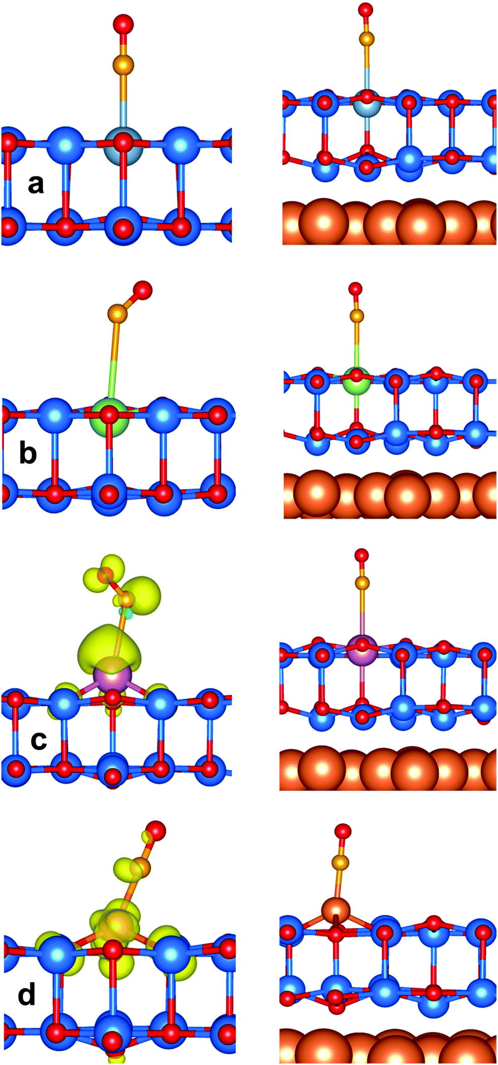 | ||
| Fig. 7 CO adsorption on unsupported ZnO (left) and ZnO/Cu(111) bilayers (right). (a) Al:ZnO; (b) Ga:ZnO; (c) In:ZnO; (d) Cu:ZnO. Zn, O, Cu, Al, Ga, In and C are blue, red, orange, light-blue, green, purple and gold spheres, respectively. Spin density (transparent yellow) is plotted with an isosurface of 0.005|e| Å−3. | ||
Next, we consider CO adsorption on neighboring Zn sites of the surface dopant, Table S1 (ESI†). For the Al- and Ga-doped ZnO bilayer, the adsorption energy is in the range of −0.3 eV to −0.5 eV; large redshifts of the CO molecule in the range of −149/−177 cm−1 are found, consistent with the fact that the excess charge provided by the Al and Ga dopants is delocalized over the conduction band of the materials.
When one considers the CO on neighboring Zn sites of Al-, or Ga-doped ZnO/Cu(111) supported films, the CO adsorption properties (adsorption energy, CO stretching frequency, bond length, and Zn–CO distance) are practically the same as on pristine ZnO/Cu(111), Table S1 (ESI†). This is a further proof that the extra electron has been transferred to the Cu support.
The situation is similar for CO adsorption on In:ZnO and In:ZnO/Cu(111), Fig. 7c. Here the CO adsorption energy is slightly larger on the supported film (−0.28 eV) than on the free-standing one (−0.13 eV). The CO stretching frequency is blue-shifted by +12 cm−1 on In:ZnO/Cu(111) and red-shifted by −160 cm−1 on In:ZnO, Table 3. The difference reflects the localization of charge on In on the unsupported layer, and the occurrence of a charge transfer to Cu on the supported layer.
When one considers CO adsorption on the Zn sites of the unsupported In:ZnO bilayer, we notice a strong dependence of the CO stretching frequency on the distance of the Zn ions where CO is adsorbed from the In dopant. For Zn ions close to the In-dopant, there is a large red-shift of −160 cm−1, while when the Zn adsorption site is far away the shift is negligible. When the supported In:ZnO film is considered, adsorption on Zn sites gives CO frequencies similar to those of the pristine film, since the excess electron has been transferred to the Cu support, Table S1 (ESI†).
The last case is that of CO adsorption on Cu ions of the Cu-doped materials, Fig. 7d. Here a significant increase in the adsorption energy is found for Cu:ZnO/Cu(111), −1.06 eV, which has to be compared with a −0.46 eV binding energy in Cu:ZnO. This is associated with a higher back donation to CO from Cu:ZnO/Cu(111), −0.16|e|, than from Cu:ZnO, −0.04|e|, resulting in a longer CO bond length (1.160 Å vs. 1.151 Å) and a bigger red shift (−83 cm−1vs. −58 cm−1), Table 3.
When CO adsorption on the nearest neighbor Zn sites is considered for Cu doping, we observed the same properties as on the undoped system. In particular, the adsorption energy is about 0.2 eV and the CO frequency is slightly redshifted (the largest redshift is −23 cm−1) in ZnO/Cu(111) and slightly blueshifted (the maximum value is +12 cm−1) in the ZnO bilayer, Table S1 (ESI†). This result confirms (a) that there is a strong localization of electrons on the Cu ion and, (b) that the hole created by Cu doping is compensated by a charge transfer from the underlying Cu support to the Cu:ZnO film.
4. Conclusions
The doping of group-III elements (Al, Ga and In) and Cu in the ZnO bilayer and ZnO/Cu(111) supported films has been studied by means of the DFT+U approach, including dispersion contribution. The charge distribution following the doping has been probed by CO adsorption.Here the following conclusions can be drawn:
• In Al:ZnO and Ga:ZnO bilayers, the excess electrons are delocalized over the conduction band according to the calculations; it should be mentioned that in a real system, the presence of point defects, grain boundaries, etc. will provide sites where the excess charge can be efficiently trapped.
• In In:ZnO, the excess charge is localized in the In dopant.
• When the supported films are considered, Al:ZnO/Cu(111), Ga:Zn/Cu(111) and In:ZnO/Cu(111), we observe that the excess electron is transferred to the Cu support. In this respect, the doped film behaves similarly to the undoped one. This is proven by the properties of the CO probe molecule. In particular, a large redshift of the CO stretching frequency is observed in the doped ZnO bilayer (due to the presence of an excess of charge in the conduction band), while this is small or negligible in the supported doped ZnO films, since the excess charge moves to the Cu support.
• In Cu:ZnO, the oxidation state of Cu is 2+, Cu(3d9) state; in Cu:ZnO/Cu(111), a charge transfer occurs from the Cu support to the Cu dopant with a change in the oxidation state, 1+, Cu(3d10). As a consequence, a stronger CO binding energy and a larger redshift of CO frequency were obtained in Cu:ZnO/Cu(111) compared to Cu:ZnO.
In conclusion, the underlying Cu support plays a different role for n-type and p-type dopants. It is compensating the charge introduced from dopants. In particular, it acts as an electron acceptor when extra electrons are generated by n-type dopants, and as an electron donor when holes are created by p-type dopants.
These general principles can be of some help in the design of new materials based on supported oxide ultrathin films for the design of more efficient sensors or heterogeneous catalysts.
Conflicts of interest
There are no conflicts of interest to declare.Acknowledgements
The work was supported by the Italian MIUR through the PRIN Project 2015K7FZLH SMARTNESS “Solar driven chemistry: new materials for photo- and electro-catalysis”. We acknowledge the CINECA facility for the availability of high-performance computing resources.References
- Ü. Özgür, Ya. I. Alivov, C. Liu, A. Teke, M. A. Reshchikov, S. Doğan, V. Avrutin, S.-J. Cho and H. Morkoç, J. Appl. Phys., 2005, 98, 041301 CrossRef.
- L. Znaidi, Mater. Sci. Eng., B, 2010, 174, 18–30 CrossRef CAS.
- M. Sahal, B. Hartiti, A. Ridah, M. Mollar and B. Marí, Microelectron. J., 2008, 39, 1425–1428 CrossRef CAS.
- M. R. Wagner, G. Callsen, J. S. Reparaz, R. Kirste, A. Hoffmann, A. V. Rodina, A. Schleife, F. Bechstedt and M. R. Phillips, Phys. Rev. B: Condens. Matter Mater. Phys., 2013, 88, 235210 CrossRef.
- C. Hirose, Y. Matsumoto, Y. Yamamoto and H. Koinuma, Appl. Phys. A: Mater. Sci. Process., 2004, 79, 807–809 CrossRef CAS.
- D.-W. Kang, S.-H. Kuk, K.-S. Ji, S.-W. Ahn and M.-K. Han, Jpn. J. Appl. Phys., 2010, 49, 031101 CrossRef.
- H. Sun, S.-U. Jen, H.-P. Chiang, S.-C. Chen, M.-H. Lin, J.-Y. Chen and X. Wang, Thin Solid Films, 2017, 641, 12–18 CrossRef CAS.
- L. Gong, J. Lu and Z. Ye, Sol. Energy Mater. Sol. Cells, 2010, 94, 1282–1285 CrossRef CAS.
- K. M. Sandeep, S. Bhat, F. J. Serrao and S. M. Dharmaprakash, AIP Conf. Proc., 2016, 1731, 080055 CrossRef.
- G. Shanmuganathan, I. B. Shameem Banu, S. Krishnan and B. Ranganathan, J. Alloys Compd., 2013, 562, 187–193 CrossRef CAS.
- D. Akcan, A. Gungor and L. Arda, J. Mol. Struct., 2018, 1161, 299–305 CrossRef CAS.
- C. H. Park, S. B. Zhang and S.-H. Wei, Phys. Rev. B: Condens. Matter Mater. Phys., 2002, 66, 073202 CrossRef.
- B. Y. Zhang, B. Yao, Y. F. Li, Z. Z. Zhang, B. H. Li, C. X. Shan, D. X. Zhao and D. Z. Shen, Appl. Phys. Lett., 2010, 97, 222101 CrossRef.
- R. Amiruddin, S. Devasia, D. K. Mohammedali and M. C. Santhosh Kumar, Semicond. Sci. Technol., 2015, 30, 035009 CrossRef.
- P. Jongnavakit, P. Amornpitoksuk, S. Suwanboonb and N. Ndiege, Appl. Surf. Sci., 2012, 258, 8192–8198 CrossRef CAS.
- A. R. Nimbalkar and M. G. Patil, Mater. Sci. Semicond. Process., 2017, 71, 332–341 CrossRef CAS.
- T. Çorlu, I. Karaduman, S. Galioglu, B. Akata, M. A. Yıldırım, A. Ates and S. Acar, Mater. Lett., 2018, 212, 292–295 CrossRef.
- P. S. Shewale, V. B. Patil, S. W. Shin, J. H. Kim and M. D. Uplane, Sens. Actuators, B, 2013, 186, 226–234 CrossRef CAS.
- N.-E. Sung, I.-J. Lee, A. Thakur, K. H. Chae, H.-J. Shin and H.-K. Lee, Mater. Res. Bull., 2012, 47, 2891–2894 CrossRef CAS.
- M. Caglar and F. Yakuphanoglu, Appl. Surf. Sci., 2012, 258, 3039–3044 CrossRef CAS.
- A. Sreedhar, J. H. Kwon, J. Yi, J. S. Kim and J. S. Gwag, Mater. Sci. Semicond. Process., 2016, 49, 8–14 CrossRef CAS.
- M. Suja, S. B. Bashar, M. M. Morshed and J. Liu, ACS Appl. Mater. Interfaces, 2015, 7, 8894–8899 CrossRef CAS PubMed.
- C. Chen, W. Dai, Y. Lu, H. He, Q. Lu, T. Jin and Z. Ye, Mater. Res. Bull., 2015, 70, 190–194 CrossRef CAS.
- D. Chakraborti and J. Narayan, Appl. Phys. Lett., 2007, 90, 062504 CrossRef.
- X. Wang, J. B. Xu, W. Y. Cheung, J. An and N. Ke, Appl. Phys. Lett., 2007, 90, 212502 CrossRef.
- D. K. Lee, J. H. Park, J. I. Choi, Y. Lee, S. J. Kim, G.-H. Lee, Y.-H. Kim and J. K. Kang, Nanoscale, 2014, 6, 10995–11001 RSC.
- R. Liu, F. Wang, A. Pan, L. Cao and Z. L. Wang, J. Phys. Chem. B, 2006, 110, 12865–12873 CrossRef PubMed.
- M. K. Gupta, J.-H. Lee, K. Y. Lee and S.-W. Kim, ACS Nano, 2013, 7, 8932–8939 CrossRef CAS PubMed.
- X.-Y. Feng, Z. Wang, C.-W. Zhang and P.-J. Wang, J. Nanomater., 2013, 6, 181979 Search PubMed.
- G. B. Lee, G. D. Han, J. H. Shim and B.-H. Choi, J. Vac. Sci. Technol., A, 2015, 33, 01A134 CrossRef.
- Z. Wang, L. Gan, H. He and Z. Ye, ACS Appl. Mater. Interfaces, 2017, 9, 13537–13543 CrossRef CAS PubMed.
- V. Schott, H. Oberhofer, A. Birkner, M. Xu, Y. Wang, M. Muhler, K. Reuter and C. Wöll, Angew. Chem., Int. Ed., 2013, 52, 11925–11929 CrossRef CAS PubMed.
- B.-H. Liu, I. M. N. Groot, Q. Pan, S. Shaikhutdinov and H.-J. Freund, Appl. Catal., A, 2017, 548, 16–23 CrossRef CAS.
- C. Tusche, H. L. Meyerheim and J. Kirschner, Phys. Rev. Lett., 2007, 99, 026102 CrossRef CAS PubMed.
- Q. Pan, B. H. Liu, M. E. McBriarty, Y. Martynova, I. M. N. Groots, S. Wang, M. J. Bedzyk, S. Shaikhutdinov and H.-J. Freund, Catal. Lett., 2014, 144, 648–655 CrossRef CAS.
- F. Tumino, C. S. Casari, M. Passoni, C. E. Bottani and A. L. Bassi, Nanotechnology, 2016, 27, 475703 CrossRef CAS PubMed.
- X. Deng, K. Yao, K. Sun, W.-X. Li, J. Lee and C. Matranga, J. Phys. Chem. C, 2013, 117, 11211–11218 CrossRef CAS.
- J. Schumann, J. Kröhnert, E. Frei, R. Schlögl and A. Trunschke, Top. Catal., 2017, 60, 1735–1743 CrossRef CAS.
- S. Kattel, P. J. Ramirez, J. G. Chen, J. A. Rodriguez and P. Liu, Science, 2017, 355, 1296–1299 CrossRef CAS PubMed.
- S. Tosoni, C. Li, P. Schlexer and G. Pacchioni, J. Phys. Chem. C, 2017, 121, 27453–27461 CrossRef CAS.
- D. Mora-Fonz, T. Lazauskas, M. R. Farrow, C. R. A. Catlow, S. M. Woodley and A. A. Sokol, Chem. Mater., 2017, 29, 5306–5320 CrossRef CAS.
- H. V. Thang, S. Tosoni and G. Pacchioni, ACS Catal., 2018, 8, 4110–4119 CrossRef CAS.
- H. V. Thang and G. Pacchioni, J. Phys. Chem. C, 2018 DOI:10.1021/acs.jpcc.8b03479.
- H. V. Thang and G. Pacchioni, J. Phys. Chem. C, 2018, 122, 20880–20887 CrossRef CAS.
- F. Stavale, X. Shao, N. Nilius, H.-J. Freund, S. Prada, L. Giordano and G. Pacchioni, J. Am. Chem. Soc., 2012, 134, 11380–11383 CrossRef CAS PubMed.
- X. Shao, S. Prada, L. Giordano, G. Pacchioni, N. Nilius and H.-J. Freund, Angew. Chem., Int. Ed., 2011, 50, 11525–11527 CrossRef CAS PubMed.
- G. Kresse and J. Furthmüller, J. Comput. Mater. Sci., 1996, 6, 15–50 CrossRef CAS.
- G. Kresse and J. Furthmüller, Phys. Rev. B: Condens. Matter Mater. Phys., 1996, 54, 11169–11186 CrossRef CAS.
- J. P. Perdew, K. Burke and M. Ernherhof, Phys. Rev. Lett., 1996, 77, 3865–3868 CrossRef CAS PubMed.
- P. E. Blöchl, Phys. Rev. B: Condens. Matter Mater. Phys., 1994, 50, 17953 CrossRef.
- G. Kresse and J. Joubert, Phys. Rev. B: Condens. Matter Mater. Phys., 1999, 59, 1758 CrossRef CAS.
- V. I. Anisimov, J. Zaanen and O. K. Andersen, Phys. Rev. B: Condens. Matter Mater. Phys., 1991, 44, 943–954 CrossRef CAS.
- S. L. Dudarev, G. A. Botton, S. Y. Savrasov, C. J. Humphreys and A. P. Sutton, Phys. Rev. B: Condens. Matter Mater. Phys., 1998, 57, 1505–1509 CrossRef CAS.
- A. Janotti and C. G. Van de Walle, Phys. Rev. B: Condens. Matter Mater. Phys., 2007, 76, 165202 CrossRef.
- R. W. G. Wyckoff, Crystal Sructures, 1963, vol. 1, pp. 85–237 Search PubMed.
- S. Grimme, J. Comput. Chem., 2006, 27, 1787–1799 CrossRef CAS PubMed.
- S. Tosoni and J. Sauer, Phys. Chem. Chem. Phys., 2010, 12, 14330–14340 RSC.
- Y. Liu and J. Lian, Appl. Surf. Sci., 2007, 253, 3727–3730 CrossRef CAS.
- R. Dhahri, M. Hjiri, L. El Mir, A. Bonavita, D. Lannazzo, M. Latino, N. Donato, S. G. Leonardi and G. Neri, J. Phys. D: Appl. Phys., 2016, 49, 135502 CrossRef.
- T. Saidani, M. Zaabat, M. S. Aida and B. Boudine, Superlattices Microstruct., 2015, 88, 315–322 CrossRef CAS.
- W. Tang, E. Sanville and G. Henkelman, J. Phys.: Condens. Matter, 2009, 21, 084204 CrossRef CAS PubMed.
- E. Sanville, S. D. Kenny, R. Smith and G. Henkelman, J. Comput. Chem., 2007, 28, 899–908 CrossRef CAS PubMed.
- G. Henkelman, A. Arnaldsson and H. Jónsson, Comput. Mater. Sci., 2006, 36, 254–360 CrossRef.
- M. Yu and D. R. Trinkle, J. Chem. Phys., 2011, 134, 064111 CrossRef PubMed.
- S. Horzum, E. Torun, T. Serin and F. M. Peeters, Philos. Mag., 2016, 96(17), 1743–1756 CrossRef CAS.
- J. Kaczkowski, Acta Phys. Pol., A, 2012, 121, 1142 CrossRef CAS.
- F. K. Shan and Y. S. Yu, J. Eur. Ceram. Soc., 2004, 24, 1869–1872 CrossRef CAS.
- Z. Xinfei, C. Hao, W. Hao, W. Rui, C. Yi, F. Qiang, Y. Fan and B. Xinhe, Acta Phys. – Chim. Sin., 2018, 34, 0001–0009 Search PubMed.
Footnote |
| † Electronic supplementary information (ESI) available. See DOI: 10.1039/c8cp06717a |
| This journal is © the Owner Societies 2019 |