
Even–odd oscillation of bandgaps in GeP3 nanoribbons and a tunable 1D lateral homogenous heterojunction
Rui
Li
a,
Xiaowei
Huang
a,
Xiaoyu
Ma
a,
Zhili
Zhu
 b,
Chong
Li
b,
Congxin
Xia
c,
Zaiping
Zeng
*a and
Yu
Jia
*ab
b,
Chong
Li
b,
Congxin
Xia
c,
Zaiping
Zeng
*a and
Yu
Jia
*ab
aKey Laboratory for Special Functional Materials of Ministry of Education, Collaborative Innovation Center of Nano Functional Materials and Applications, and School of Materials Science and Engineering, Henan University, Kaifeng, Henan 475001, China. E-mail: zaiping.zeng@henu.edu.cn; jiayu@henu.edu.cn
bInternational Laboratory for Quantum Functional Materials of Henan, and School of Physics and Engineering, Zhengzhou University, Zhengzhou, Henan 450001, China
cCollege of Physics and Materials Science, Henan Normal University, Xinxiang, Henan 453007, China
First published on 20th November 2018
Abstract
GeP3 is a new kind of IV–V two dimensional material that has been predicted very recently. Here, we have theoretically explored the electronic properties of GeP3 nanoribbons (NRs) by employing first-principles calculations within density functional theory. We find that, unlike other monolayer materials, the bandgaps of armchair GeP3 NRs exhibit a strong even–odd oscillation as a function of nanoribbon width and such oscillations can remain intensive even when the width reaches up to 9 nm. The underlying physics of such oscillation originates from both the parity-dependent geometric symmetry and quantum size effects. Furthermore, we also find that suitable chemical decoration at the nanoribbon edge, e.g., by passivating hydrogen atoms, effectively tunes the indirect band gap into a direct one, making these nanoribbons potentially important for photovoltaic applications. Based on the strong bandgap oscillating nature of GeP3 NRs, we have conceptually designed a lateral homogenous heterojunction, constructed by GeP3 nanoribbons with different widths, which has shown a type-II band alignment beneficial for photo-detector applications.
1 Introduction
Since the discovery of graphene, the family of two-dimensional (2D) materials has been considerably enriched, offering nearly all desirable electronic properties that are required for electronics and optoelectronics.1–3 Although graphene and the “post-graphene” materials of group IV, such as silicene and germanene, possess ultrahigh mobility and good air stability, they are semi-metallic and lack an intrinsic band gap, consequently limiting their device applications.4–7 For example, field-effect transistors (FETs) based on graphene usually exhibit very low on/off ratios and photodetectors based on graphene always yield a very high dark current and poor photo-response.8–11 On the other hand, 2D materials of group V, such as black phosphorene (BP), have a tunable band gap ranging from 0.59 eV for the five-layer to 1.51 eV for the monolayer.12 Based on its high hole mobility, BP has shown great promise in the applications of FETs,13 photodetectors,14 and solar cells.15 Although various excellent properties have been delivered, BP still suffers from being unstable,16 therefore limiting its practical applications. It is naturally expected that a possible combination of a group IV element and a group V element would inherit their parental advantages.Monolayer germanium phosphide (GeP), as a typical group IV–V compound, has been theoretically predicted to possess a stable structure and experimentally proved to exhibit extraordinary electronic properties.11,17,18 It has a tunable band gap from 1.68 eV for the monolayer to 0.51 eV for the bulk.11 Thin GeP shows strong anisotropy of phonon vibrations and photodetectors based on GeP flakes show highly anisotropic behaviour with anisotropic factors of 1.52 and 1.83 for conductance and photo-responsivity, respectively.11 Another phase with stoichiometry, namely GeP3, could also be realized experimentally by controlling the reaction conditions.19,20 Bulk GeP3 is known to possess a puckered arsenic-type honeycomb structure with ABC stacking. It has a metallic feature and crystalizes in a layered structure.19,20 Going from bulk to 2D, 2D GeP3 appears to be semiconducting, and it possesses a low indirect band gap of 0.55 eV for the monolayer and 0.43 eV for the bilayer, and high carrier mobilities comparable to those of phosphorene.17 Due to its excellent properties, 2D GeP3 has been characterized as a high capacity electrode material for Li-ion batteries.21–23 Wang et al. studied the transport properties of GeP3 and the transmission coefficient T (E) is sensitive to the connecting formation between the central monolayer GeP3 nanoribbon and trilayer GeP3 nanoribbon at both ends.24 Cutting a monolayer into a nanometer scale width leads to the formation of a new category of quasi-1D materials, namely nanoribbons (NRs). Compared to the monolayer, NRs are found to exhibit many more unique properties due to the existence of the edge states and size effects. Graphene NRs with zigzag edges exhibit special localized edge states, resulting in a very different magnetic order (ferromagnetic (FM) order vs. antiferromagnetic (AFM) order).25 Their armchair counterparts have demonstrated a period oscillation in the band gap, which decays rapidly with increased width.26,27 On the other hand, the geometric width and configuration of atoms along the long edges offer fresh freedom of manipulation in the electronic properties of phosphorene NRs.28 In contrast to the multiple studies on group IV and V 2D materials, the electronic properties of the newly explored group IV–V 2D materials, namely GeP3, are far less understood.
In this contribution, we explore the electronic properties of GeP3 nanoribbons by means of first-principles density-functional theory calculations. We have found that GeP3 NRs with zigzag edges demonstrate a semiconductor feature with an indirect gap. This gap rapidly decreases with increased nanoribbon width. Their armchair counterparts also present a semiconducting feature and the gap exhibits a strong even–odd oscillation as a function of nanoribbon width. In particular, such oscillations remain intensive even when the width reaches up to 9 nm, being much stronger than those of its group IV counterparts. Interestingly, we find that passivating the nanoribbon edges with hydrogen atoms effectively tunes the indirect band gap into a direct one, making these nanoribbons potentially important for photovoltaic applications. Based on the strong oscillating nature of GeP3 NRs, we have further designed a lateral homogenous heterojunction, constructed by GeP3 nanoribbons with different widths, which has shown a type-II band alignment being beneficial for photo-detector applications.
2 Computational details
All calculations are performed by using the first-principles method within the framework of density functional theory (DFT),29,30 as implemented in the Vienna ab initio simulation package (VASP).31,32 For 2D materials, it is known that the vdW interaction and spin orbital coupling (SOC) are essential to get more accurate results.33,34 Here, we have employed the projector augmented wave (PAW) pseupotentials35,36 and the exchange–correlation potential is approximated by the generalized gradient approximation (GGA) using the PBE (Perdew–Burke–Ernzerhof) functional.37 Further, vdW corrections as proposed by Grimme (PBE + D2)38,39 were also employed to describe the weak interactions in GeP3 nanoribbons. As for the spin orbit coupling, we have checked the band structure calculations with and without SOC, and the results show that the SOC has almost no influence on the band structures. So, we present our results without SOC in the following. The plane-wave kinetic energy cut-off is chosen to be 500 eV. The Brillouin zone (BZ) integration was undertaken on top of 1 × 9 × 1 k-meshes for armchair nanoribbons and 9 × 1 × 1 k-meshes for zigzag nanoribbons. Periodic boundary conditions were applied. A vacuum space of ∼20 Å was included in the simulation cell in order to eliminate the interaction between the simulation cell and its images. The energy convergence threshold was set to be 10−4 eV until the residual atomic forces reach below 0.02 eV Å−1. Due to the heavier computational load, only partial calculations were performed using the Heyd–Scuseria–Ernzerhof hybrid functional (HSE06) with 25% Hatree–Fock exchange–correlation energy, which gives a better description of the band gap.40 For the final simulation of the designed lateral homogenous heterojunctions, we adopted a supercell of 45 Å × 48 Å × 20 Å. Considering the supercell size in real space and available computational resources, the k-mesh was chosen as 1 × 2 × 1 and the convergence threshold of forces was set to be 0.05 eV Å−1. To check the stability of the nanoribbons, we tend to evaluate the edge energy, which is defined as| Eedge = (Eribbon − nEunit − mμGe − kμP − hμH)/2L, | (1) |
3 Results and discussion
3.1 Electronic properties of zigzag GeP3 nanoribbons
We start the exploration of the electronic properties of GeP3 nanoribbons with zigzag edges (e.g., cf.Fig. 1(a)). When cutting a nanoribbon from a GeP3 monolayer, three configurations could be reached depending on the atom types at the edges: (i) nanoribbons ending with Ge and P atoms at both edges, (ii) nanoribbons ending with Ge and P atoms at one edge and with P atoms at the other edge, and (iii) nanoribbons ending with P atoms at both edges. To find the energetically most stable configuration, we computed the edge energy according to eqn (1) for each configuration, considering different nanoribbon widths. It turns out that the nanoribbons with configuration (i) have the lowest edge energy, therefore being energetically favorable, irrespective of the nanoribbon width. Consequently, we focus hereafter only on this configuration.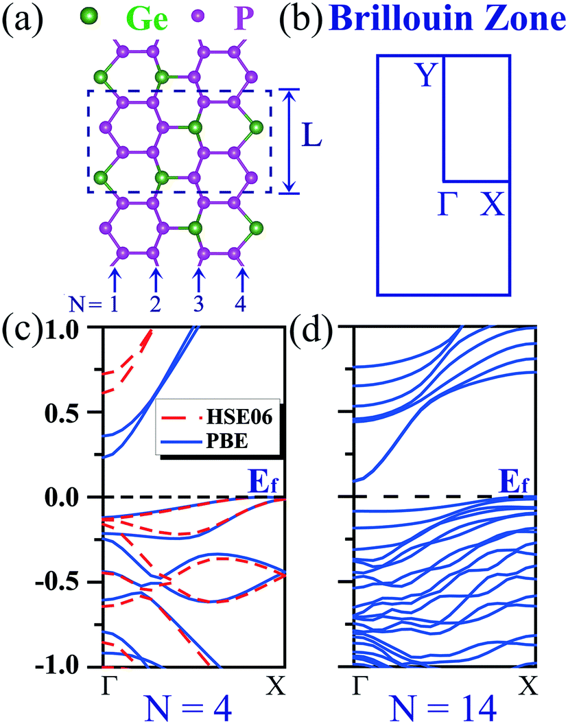 | ||
| Fig. 1 (a) Top view of the optimized geometry of a zigzag-edged GeP3 nanoribbon with width N = 4, where N is indicated below. The dashed rectangular box indicates the unit cell employed in the simulation. (b) Brillouin zone of the nanoribbon. (c and d) Computed band structures of zigzag-edged GeP3 nanoribbon with (c) N = 4 and (d) N = 14, respectively. The band structures in red and blue color were calculated by the HSE06 and PBE methods, respectively. | ||
In the absence of spin-polarization, zigzag nanoribbons made of only group IV elements (e.g., graphene)25,41,42 or only P elements28 are often metallic. Strikingly, we find that their GeP3 counterparts of group IV–V appear to be semiconducting, exhibiting an indirect gap (cf.Fig. 1(c and d)). Due to the strong quantum confinement effects, the narrowest nanoribbon turns out to have the largest gap, which is around 0.23 eV. However, it decreases rapidly with increasing nanoribbon width and the gap drops into the sub-0.1 eV scale (cf.Fig. 1(d)), being nearly metallic. It is well known that the PBE functional tends to significantly underestimate the band gap. Therefore, we have further computed the band structure of the two narrowest zigzag NRs (e.g., N = 4 and 5) by using the hybrid functional HSE06. We find that the gap is significantly enlarged. It becomes 0.61 eV for N = 4 and drops rapidly to 0.14 eV for N = 5. It is well-known that calculations for larger sizes with the HSE06 functional are certainly more computationally demanding. Consequently, we focus only on relatively small systems that are allowed by our computational resources throughout the work.
3.2 Electronic properties of armchair GeP3 nanoribbons
We proceed to study the electronic properties of armchair GeP3 nanoribbons. Armchair nanoribbons also exhibit three different configurations, depending on the atom types at the edges, similar to their zigzag counterparts. It is found that the nanoribbons with edges including Ge atoms are significantly distorted due to the edge reconstructions (e.g., configurations (i) and (ii)), while the edge reconstruction is far less in the ones ending with only P atoms at both edges, which show a very similar structure to their monolayer parentage (cf.Fig. 2(a)). We have therefore further computed the edge energy as a function of the nanoribbon width (cf.Fig. 2(b)). It was found that the edge energy decreases nearly linearly, accompanied by an even–odd oscillating feature, as the size of the nanoribbon increases. This suggests that the edge stability dominantly affects the overall stability, especially for narrower nanoribbons, since the nanoribbons are composed of a significant amount of edge atoms. However, decorating the edges with hydrogen (e.g., H-passivation) atoms effectively saturates the dangling bonds and the nanoribbons become more stable. Besides improving the stability, hydrogen decoration will considerably affect the electronic properties of the nanoribbons, which we shall see later on. | ||
| Fig. 2 (a) Top and side views of the optimized geometry structure of our largest armchair GeP3 nanoribbon with width N = 15, where N represents half the total number of dimers appearing along the zigzag direction. The dashed rectangular box indicates the unit cell employed in the simulation. (b) Computed edge energy as a function of the width for both unpassivated (e.g., bare) and hydrogen-passivated (e.g., H-passivated) nanoribbons. | ||
On top of the stability study, we proceed to explore the band structures of GeP3 nanoribbons and compare them with the available ones of group IV or V. The band gap as a function of nanoribbon width is presented in Fig. 3(a). It is found that the gap decreases with increasing width due to the reduction of quantum confinement effects. Such a decrease is accompanied by a strong even–odd oscillation. This feature has also been found in other nanoribbons of group IV (e.g., graphene).26,27,43 In contrast to the rapid reduction of the oscillating amplitude in group IV, the even–odd oscillation in the gap of GeP3 remains very intensive even when the nanoribbon reaches up to 5 nm in width (cf.Fig. 3(a)). For un-passivated nanoribbons, the valence band maximum (VBM) is found to always be located at the Y-point (cf.Fig. 3(b)). However, the location of the conduction band minimum (CBM) is width-dependent. It is at the Γ-point for width N being odd (e.g., N = 7), while it is at a position along the Γ–Y line for N being even (e.g., N = 8, cf.Fig. 3(b)). Through a careful analysis of the partial density of states, we find that both the valence band maximum (VBM) and conduction band minimum (CBM) are dominantly contributed from the 2p-orbital (mainly pz) of P atoms, which is consistent with their monolayer parentage.17 The even–odd oscillation might be attributed to the nanoribbons' geometric symmetry. Indeed, we find that the symmetry is C2h when the nanoribbon width N is even, while it reduces to Cs when N is odd. Naturally, the gap is expected to reach the limit of its monolayer parentage as the width keeps increasing and approaches infinity. However, for the un-passivated nanoribbons, the gaps appear to be well below the expected 2D limit (∼0.26 eV at the PBE level) even for the nanoribbons in the regime of very strong quantum confinement (e.g., N = 5). After a careful examination of the charge density distribution, it turns out that the CBM state of the un-passivated nanoribbon is localized around the center of the nanoribbon, while its VBM state is found to be a dangling bond state, which in turn causes a gap much smaller than the 2D limit.
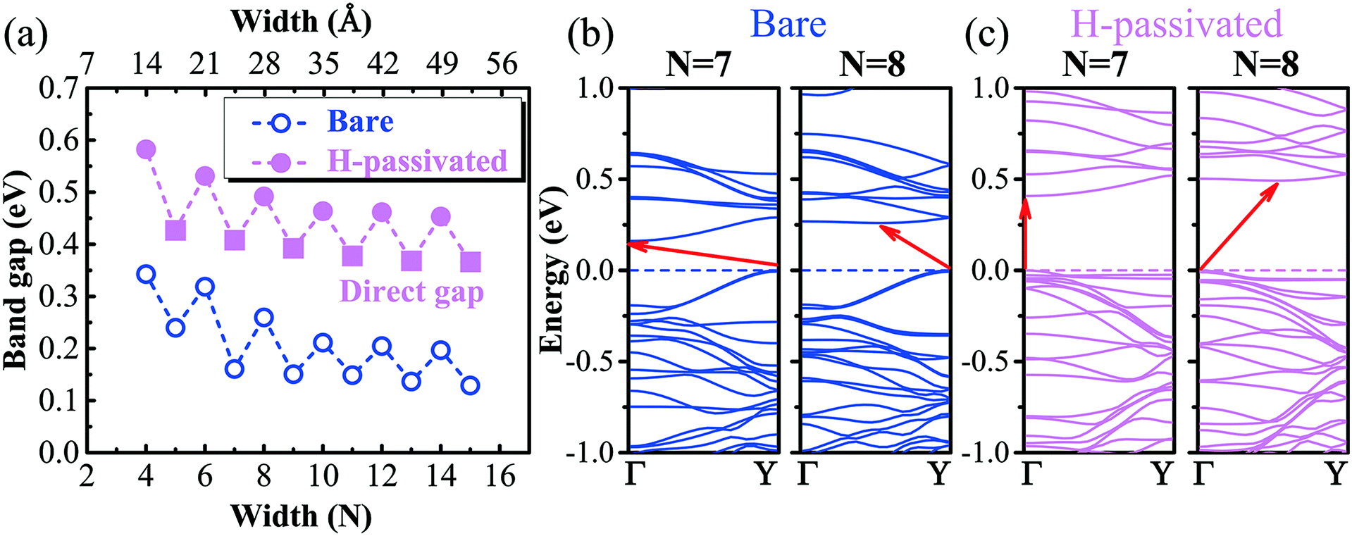 | ||
| Fig. 3 (a) Band gap of armchair GeP3 nanoribbons as a function of the width. The circles represent an indirect gap, while the squares represent a direct gap. (b) and (c) are the band structures for un-passivated and H-passivated nanoribbons with width N = 7 and 8, respectively. The valence band maximum is chosen as the reference energy. Γ and Y are the high-symmetry points of the Brillouin zone presented in Fig. 1(b). | ||
Decorating the nanoribbon edges with hydrogen atoms significantly increases the gap, partially due to the saturation of the aforementioned dangling bonds, which can be confirmed by the disappearance of the VBM and its neighbouring valence band states (cf.Fig. 3(b and c)). However, the even–odd oscillating feature remains. Strikingly, compared to the un-passivated nanoribbons, the decorated ones exhibit a direct gap when width N is odd. Both the valence band maximum (VBM) and conduction band minimum (CBM) are located at the Γ-point of the Brillouin zone (cf.Fig. 1(b)), which might drastically enhance the light absorption. For nanoribbons with width N being even, the indirect gap feature remains, where the VBM is at the Γ-point and the CBM is located at the mid-way of the Γ–Y line. Tuning the indirect gap to a direct one has been previously achieved in a GeP3 monolayer by applying biaxial strain.17 Our results therefore suggest a much simpler way of reaching the direct gap feature in GeP3 2D systems by finely controlling the nanoribbon size, simultaneously with tunable energies, which should be very promising in photovoltaic applications.
The decrease in the gap for both unpassivated and H-terminated nanoribbons appears to be quite slow. To this end, we have further computed the band structure of a nanoribbon with width N = 26 (∼9 nm) and terminated by H-atoms, which is the largest size we could computationally afford. Comparing to our narrowest nanoribbon, the gap only decreases by less than 30%. This suggests a large electron Bohr radius as well as a large electron mean free path for the GeP3 nanoribbons. To obtain a better quantitative result, we have performed further calculations of the band structure properties of nanoribbons with N = 4, 5, 6, and 7, respectively, by using the HSE06 hybrid functional. The gaps are significantly enlarged due to a better description of the exchange–correlation energy, reaching up to 0.92, 0.72, 0.86 and 0.70 eV, respectively. This suggests that the GeP3 nanoribbons might find applications in infrared detection.
3.3 Size tunable one-dimensional lateral homogenous heterojunction
Finally, based on the strong even–odd oscillating nature of the GeP3 nanoribbon, we further designed a lateral homogenous heterojunction using two flakes of nanoribbons, where one nanoribbon's width is even, while the width of the other one is odd. An (m, n)-junction is therefore employed to denote the constructed heterojunction. The nanoribbon with width m has a smaller band gap than the one with width n. Considering the limitation of the computational resources, we only take the (7, 4)-junction as an example to investigate the properties of heterojunctions. The results are shown in Fig. 4. | ||
| Fig. 4 (a) The projected band structure of a (7, 4)-junction constructed by two nanoribbons with width N = 7 and 4. (b) The partial charge density of the band edge states. The isosurface value is 10−3 e Å−3. (c) Schematic representation of the band alignment of the constructed (7, 4)-homojunction. | ||
We find that the charge density of the lowest conduction band state is localized in the wider region (N = 7) and the charge density of the highest valence band state is localized in the narrower region (e.g., N = 4, cf.Fig. 4(b)). The electrostatic potential analysis also demonstrates that the nanoribbon with width N = 7 has a deeper potential and the electrons will easily transfer to this region (cf.Fig. 4(c)). Fig. 4 shows a type-II band alignment for the heterojunction and it could separate the electrons and holes effectively due to the conceptually designed homogenous heterostructure, which is important for photovoltaic application. Upon varying the geometric factor (i.e., width n or m) of the heterostructure, the conduction band offset (CBO) and valence band offset (VBO) can be easily manipulated, therefore reaching a size-tunable one-dimensional lateral homogenous heterojunction. We note that such a heterojunction is built on the basis of the unique strong oscillating nature of GeP3 nanoribbons. It will not be realized in other two-dimensional material systems (e.g., graphene, black phosphorene), where such a strong oscillation in the band gap is not available.
4 Conclusions
To summarize, we have systematically explored the electronic properties of GeP3 nanoribbons of group IV–V by means of first-principles calculations. We have demonstrated that the armchair GeP3 NRs present a semiconducting feature with an indirect band gap. Moreover, the bandgaps exhibit strong even–odd oscillations as a function of nanoribbon width, which remains intensive even when the width reaches up to 9 nm because of both the parity-dependent geometric symmetry of nanoribbons and quantum size effects. We further find that suitable chemical decoration at the nanoribbon edge, e.g., by passivating hydrogen atoms, effectively tunes the indirect band gap into a direct one, making these nanoribbons potentially important for photovoltaic applications. Based on the strong oscillating nature of GeP3 NRs, we designed a lateral homogeneous heterojunction, constructed by GeP3 nanoribbons with different widths, which has shown a type-II band alignment being beneficial for photo-detector applications. The results presented herein are not only useful for the fundamental study of electronic properties, but also important for potential device applications based on the newly discovered group IV–V GeP3 2D systems.Conflicts of interest
There are no conflicts to declare.Acknowledgements
This work is supported by the NSFC (No. 11774078 and 11804077) and by Innovation Scientists and Technicians Troop Construction Projects of Henan Province (Grant No. 10094100510025). Z. Z. acknowledges the “Distinguished Professor” starting grant of Henan University with grant no. 2018001T for financial support.Notes and references
- K. S. Novoselov, A. K. Geim, S. V. Morozov, D. Jiang, Y. Zhang, S. V. Dubonos, I. V. Grigorieva and A. A. Firsov, Science, 2004, 306, 666–669 CrossRef CAS.
- M. J. Allen, V. C. Tung and R. B. Kaner, Chem. Rev., 2010, 110, 132–145 CrossRef CAS PubMed.
- C. Rao, A. Sood, K. Subrahmanyam and A. Govindaraj, Angew. Chem., Int. Ed., 2009, 48, 7752–7777 CrossRef CAS PubMed.
- P. Vogt, P. De Padova, C. Quaresima, J. Avila, E. Frantzeskakis, M. C. Asensio, A. Resta, B. Ealet and G. Le Lay, Phys. Rev. Lett., 2012, 108, 155501 CrossRef PubMed.
- C.-C. Liu, W. Feng and Y. Yao, Phys. Rev. Lett., 2011, 107, 076802 CrossRef PubMed.
- M. E. Davila, L. Xian, S. Cahangirov, A. Rubio and G. L. Lay, New J. Phys., 2014, 16, 095002 CrossRef.
- Z. Ni, Q. Liu, K. Tang, J. Zheng, J. Zhou, R. Qin, Z. Gao, D. Yu and J. Lu, Nano Lett., 2012, 12, 113–118 CrossRef CAS PubMed.
- I. Meric, M. Y. Han, A. F. Young, B. Ozyilmaz, P. Kim and K. L. Shepard, Nat. Nanotechnol., 2008, 3, 654 CrossRef CAS PubMed.
- F. Xia, T. Mueller, Y.-M. Lin, A. Valdes-Garcia and P. Avouris, Nat. Nanotechnol., 2009, 4, 839 CrossRef CAS PubMed.
- B. Y. Zhang, T. Liu, B. Meng, X. Li, G. Liang, X. Hu and Q. J. Wang, Nat. Commun., 2013, 4, 1811 CrossRef PubMed.
- L. Li, W. Wang, P. Gong, X. Zhu, B. Deng, X. Shi, G. Gao, H. Li and T. Zhai, Adv. Mater., 2018, 30, 1706771 CrossRef PubMed.
- J. Qiao, X. Kong, Z. Hu, F. Yang and W. Ji, Nat. Commun., 2014, 5, 4475 CrossRef CAS PubMed.
- Z. Yang, J. Hao, S. Yuan, S. Lin, H. M. Yau, J. Dai and S. P. Lau, Adv. Mater., 2015, 27, 3748–3754 CrossRef CAS PubMed.
- X. Yu, S. Zhang, H. Zeng and Q. J. Wang, Nano Energy, 2016, 25, 34–41 CrossRef CAS.
- W. Hu, L. Lin, C. Yang, J. Dai and J. Yang, Nano Lett., 2016, 16, 1675–1682 CrossRef CAS PubMed.
- J. O. Island, G. A. Steele, H. S. J. van der Zant and A. Castellanos-Gomez, 2D Mater., 2015, 2, 011002 CrossRef.
- Y. Jing, Y. Ma, Y. Li and T. Heine, Nano Lett., 2017, 17, 1833–1838 CrossRef CAS PubMed.
- P. Li, W. Zhang, D. Li, C. Liang and X. C. Zeng, ACS Appl. Mater. Interfaces, 2018, 10, 19897–19905 CrossRef CAS PubMed.
- J. Gullman and O. Olofsson, J. Solid State Chem., 1972, 5, 441–445 CrossRef CAS.
- P. C. Donohue and H. S. Young, J. Solid State Chem., 1970, 1, 143–149 CrossRef CAS.
- C. Zhang, Y. Jiao, T. He, F. Ma, L. Kou, T. Liao, S. Bottle and A. Du, Phys. Chem. Chem. Phys., 2017, 19, 25886–25890 RSC.
- D. Kim, K. Zhang, J.-M. Lim, G.-H. Lee, K. Cho, M. Cho and Y.-M. Kang, Mater. Today Energ., 2018, 9, 126–136 CrossRef.
- W. Qi, H. Zhao, Y. Wu, H. Zeng, T. Tao, C. Chen, C. Kuang, S. Zhou and Y. Huang, Sci. Rep., 2017, 7, 43582 CrossRef PubMed.
- Q. Wang, J.-W. Li, B. Wang and Y.-H. Nie, Front. Phys., 2018, 13, 138501 CrossRef.
- K. Wakabayashi, M. Fujita, H. Ajiki and M. Sigrist, Phys. Rev. B: Condens. Matter Mater. Phys., 1999, 59, 8271–8282 CrossRef CAS.
- V. Barone, O. Hod and G. E. Scuseria, Nano Lett., 2006, 6, 2748–2754 CrossRef CAS PubMed.
- Y.-W. Son, M. L. Cohen and S. G. Louie, Phys. Rev. Lett., 2006, 97, 216803 CrossRef PubMed.
- H. Guo, N. Lu, J. Dai, X. Wu and X. C. Zeng, J. Phys. Chem. C, 2014, 118, 14051–14059 CrossRef CAS.
- W. Kohn and L. J. Sham, Phys. Rev., 1965, 140, A1133–A1138 CrossRef.
- P. Hohenberg and W. Kohn, Phys. Rev., 1964, 136, B864–B871 CrossRef.
- G. Kresse and J. Furthmüller, Phys. Rev. B: Condens. Matter Mater. Phys., 1996, 54, 11169–11186 CrossRef CAS.
- G. Kresse and J. Hafner, Phys. Rev. B: Condens. Matter Mater. Phys., 1993, 47, 558–561 CrossRef CAS.
- S. Barraza-Lopez, T. P. Kaloni, S. P. Poudel and P. Kumar, Phys. Rev. B: Condens. Matter Mater. Phys., 2018, 97, 024110 CrossRef.
- E. Andharia, T. P. Kaloni, G. J. Salamo, S.-Q. Yu, H. O. H. Churchill and S. Barraza-Lopez, Phys. Rev. B: Condens. Matter Mater. Phys., 2018, 98, 035420 CrossRef.
- P. E. Blöchl, Phys. Rev. B: Condens. Matter Mater. Phys., 1994, 50, 17953–17979 CrossRef.
- G. Kresse and D. Joubert, Phys. Rev. B: Condens. Matter Mater. Phys., 1999, 59, 1758–1775 CrossRef CAS.
- J. P. Perdew, K. Burke and M. Ernzerhof, Phys. Rev. Lett., 1996, 77, 3865–3868 CrossRef CAS PubMed.
- S. Grimme, J. Comput. Chem., 2006, 27, 1787–1799 CrossRef CAS PubMed.
- S. Grimme, J. Comput. Chem., 2004, 25, 1463–1473 CrossRef CAS PubMed.
- J. Heyd, J. E. Peralta, G. E. Scuseria and R. L. Martin, J. Chem. Phys., 2005, 123, 174101 CrossRef PubMed.
- Y. Ding and J. Ni, Appl. Phys. Lett., 2009, 95, 083115 CrossRef.
- M. Monshi, S. M. Aghaei and I. Calizo, RSC Adv., 2017, 7, 18900–18908 RSC.
- S. Cahangirov, M. Topsakal and S. Ciraci, Phys. Rev. B: Condens. Matter Mater. Phys., 2010, 81, 195120 CrossRef.
| This journal is © the Owner Societies 2019 |