
Rational design and observation of the tight interface between graphene and ligand protected nanocrystals†
Byung Hyo
Kim
 a,
Hyeonhu
Bae
b,
Hyesung
Park
c,
Hoonkyung
Lee
b,
Peter
Ercius
*d and
Jungwon
Park
*ae
a,
Hyeonhu
Bae
b,
Hyesung
Park
c,
Hoonkyung
Lee
b,
Peter
Ercius
*d and
Jungwon
Park
*ae
aCenter for Nanoparticle Research, Institute for Basic Science (IBS), Seoul 08826, Republic of Korea
bDepartment of Physics, Konkuk University, Seoul 05029, Republic of Korea
cDepartment of Energy Engineering, School of Energy and Chemical Engineering, Low Dimensional Carbon Materials Center, Perovtronic Research Center, Ulsan National Institute Science and Technology (UNIST), Ulsan 44919, Republic of Korea
dNational Center for Electron Microscopy, Molecular Foundry, Lawrence Berkeley National Laboratory, Berkeley, CA 94720, USA. E-mail: percius@lbl.gov
eSchool of Chemical and Biological Engineering, Institute of Chemical Process, Seoul National University, Seoul 08826, Republic of Korea. E-mail: jungwonpark@snu.ac.kr
First published on 22nd November 2018
Abstract
Heterostructures constructed of graphene and colloidal nanocrystals provide a unique way to exploit the coupled physical properties of the two functional building blocks. Studying the interface structure between the two constituent materials is important to understand the formation mechanism and the resulting physical and chemical properties. Along with ab initio calculations, we elucidate that the bending rigidity and the strong van der Waals interaction of graphene to the metal surface guide the formation of a tight and conformal interface. Using theoretical foundations, we construct colloidal nanocrystal–graphene heterostructures with controlled interfacial structures and directly investigate the cross-sectional structures of them at high resolution by using aberration-corrected transmission electron microscopy. The experimental method and observations we present here will link the empirical methods for the formation of nanocrystal–graphene heterostructures to the mechanistic understanding of their properties.
1. Introduction
Graphene is a 2D material that can be used to design heterostructures with varied properties. The coupled physical and chemical properties of such heterostructures are determined by the choice of constituent materials and their interfacial structures driven by surface forces. Since graphene is a one atom-thick film, all constituent atoms participate in interactions with the other materials at the interface. Graphene also has a low out-of-plane stiffness compared to other materials, and as a result, it can closely conform to the surface of other materials.1–5 In addition, control over the number of layers in a multi-layer graphene film by chemical vapor deposition growth provides a way to tune the adhesion energy and stiffness when contacting with the other materials.3,6 An adhesion energy of 0.45 J m−2 for a single layer and 0.31 J m−2 for 2 to 5 layers has been determined from the atomic force microscopy measurements of bulged and delaminated graphene.7 The combination of high adhesion energy and low stiffness of graphene can be used to control the surface conformality. Scanning probe and atomic force microscopy experiments have provided the nanoscale details of the 2-dimensional surface of graphene coated on different substrates.3–6 Theoretical calculations and modelling have further provided estimations of the relevant physical parameters to understand interactions between graphene and nanomaterials depending on the types of surface forces, surface roughness, and the number of graphene layers.8–13However, in many examples of heterostructures used as catalysts and in electronic devices, the surface of the constituent nanomaterial is not bare, protected by stabilizing reagents used in the synthesis. For example, solution-synthesized nanocrystals are covered with stabilizing organic ligands which are expected to affect interfacial interactions between graphene and the nanocrystals.2 In this scenario, the interface structure will be further complicated by the presence of another interlayer with different mechanical and chemical properties from both the substrate and the graphene. The organic ligands on the nanocrystals typically affect the charge transfer dynamics at the interface of heterostructures.14,15 In contrast, formation of a tight interface presumably promotes the electron transfer between graphene and nanocrsytals.16 Therefore, direct observation of the interface structures between graphene and nanocrystals is an important step for the development of the controlled heterostructured devices. In addition, careful theoretical evaluation regarding thermodynamic aspects that play critical roles in the formation of heterostructures can be elaborated and used to design heterostructures with a desired interfacial structure. Important factors to construct a heterostructure include the binding energy of organic ligands to the substrate, the binding energy of graphene to the substrate, and the overall trend of those energies depending on the ligand coverage. Direct observation at the atomic-scale of the interface between graphene and an underlying material can also answer important questions about the local structure and separation at different locations of the interface between the two materials, which result from the interplay of adhesion energy, stiffness, morphology, and surface roughness. Nonetheless, most microscopy techniques are unable to directly observe the structure of graphene interfaces due to a discrepancy which arises from the 2-dimenstional nature of the graphene–substrate interface and the working principles of microscopy tools. They are usually used to acquire a top-down projection of the structure, not a cross-section, and thus the interface is obscured in projection due to overlapping features.
Here, we first build a theoretical foundation via ab initio calculations that show strong interactions between graphene and the metal nanocrystal surface which promote a tight contact between themselves by substituting for the surface ligands of the nanocrystal. Based on the calculations, we prepare heterostructures with an interface of solution-synthesized metal nanocrystals that mimic typical nanoscale topology with various numbers of graphene sheets to study their interfacial properties at high resolution by aberration-corrected TEM. The geometry of the heterostructures is designed to present the graphene–nanocrystal interface parallel to the imaging direction of aberration-corrected TEM, consequently, allowing direct structural investigation at the atomic-scale. We also found that the mechanical elasticity of multi-layer graphene, as controlled by the number of layers, determines the degree of conformality between the two constituent materials.
2. Results and discussion
2.1. Theoretical calculation
We perform density functional theory (DFT)17 calculations for the binding energies of surface ligands and graphene to the surface of a nanoparticle.18–20 The obtained information is used to construct the desired interface structures in graphene–metal nanoparticle heterostructures. As a model, heterostructures of graphene and silver (Ag) nanocrystals are studied because of their potential applicability in high-performance conductors and catalysts.21 We quantitatively compare the binding energy on the Ag surface of graphene and poly vinylpyrollidone (PVP), which is widely used ligands for metal nanocrystals (Fig. 1). In an optimized geometry, the PVP monomers bind to the (111) and (100) surfaces of Ag mainly with a strong interaction by the oxygen atom of the 1-ethyl-2-pyrrolidone group. The calculated binding energy of the PVP monomers with the (111) and (100) surfaces of Ag decreases as the surface coverage by the monomers decreases. We also calculate the binding energy of graphene under the same condition and obtained 11.6 meV Å−2. This value has an overlap with the binding energy of the PVP monomer group when the surface ligand density is 0.012 Å−2, implying that the surface binding energy of graphene can overcome the surface stabilization energy accomplished by PVP ligands. Therefore, forming the interface directly with graphene becomes thermodynamically more favored when the ligand coverage is below this coverage.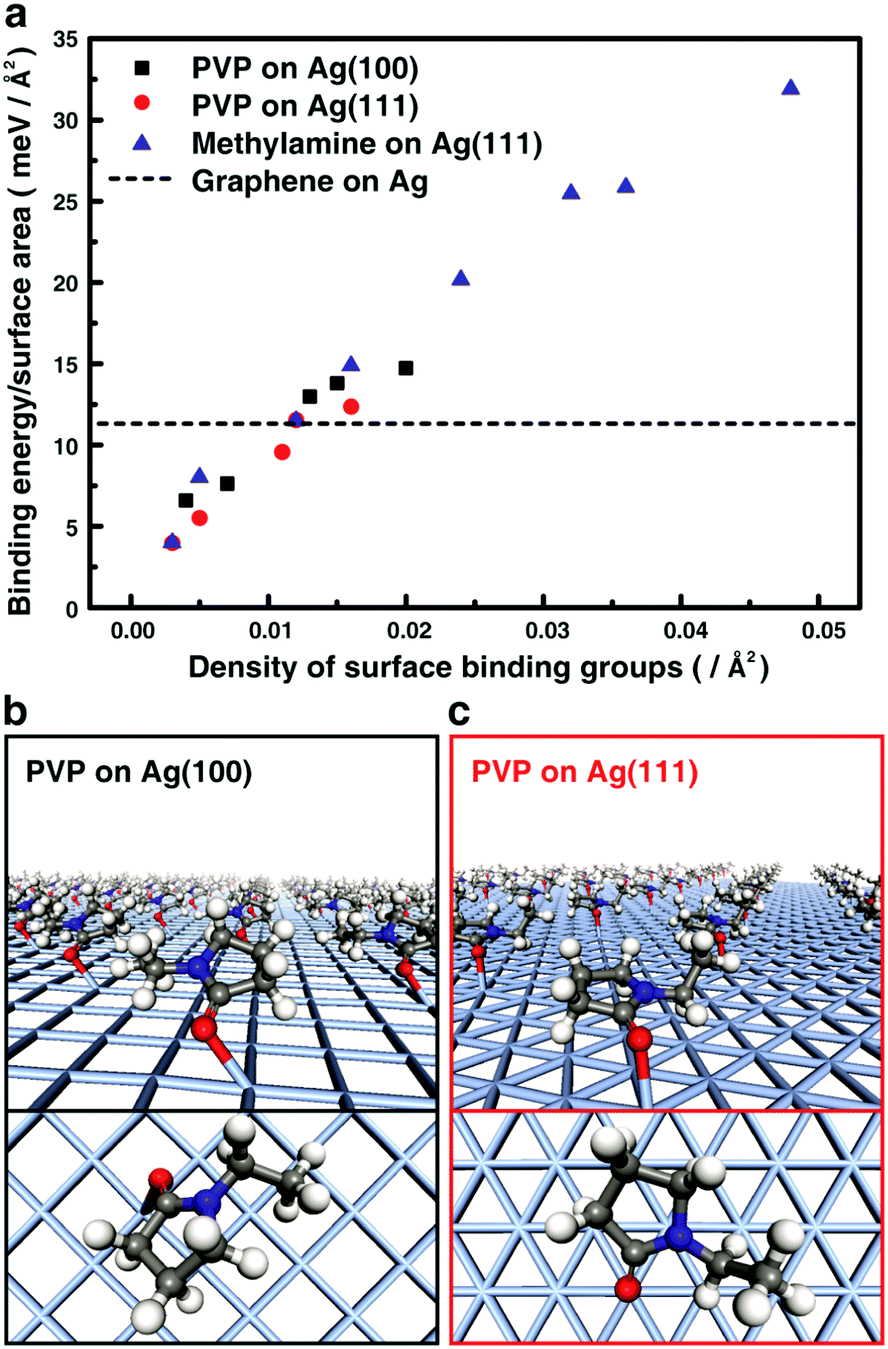 | ||
| Fig. 1 DFT calculation on the binding energy of surface ligand and graphene to the Ag nanocrystal surface. (a) Calculated surface binding energy of the functional groups on the (100) and (111) facets of an Ag nanocrystal as a function of the density of surface binding groups. (b and c) Optimized geometries of 1-ethyl-2-pyrrolidone (a single unit of polyvinylpyrrolidone (PVP) surface ligand) on the (b) (100) and (c) (111) facets of an Ag nanocrystal. Tilted view of multiple binding groups and magnified projection view on the (100) and (111) Ag surfaces are shown on top and bottom images, respectively. | ||
Since van der Waals (vdW) interactions are the dominant force between graphene and nanocrystals, the vdW interactions should be considered to confirm the possibility of forming the graphene–nanocrystal heterostructures. To investigate the effects of the vdW interaction, we also carried out calculations with LDA + D2 which include a dispersion correction for the vdW interaction.22 The vdW correction increases the binding energies between graphene and the Ag surface from 11.6 meV Å−2 to 42.3 meV Å−2 (Fig. S1, ESI†). As a result of the vdW correction, the binding energy between graphene and the Ag surface is greater than that between the PVP monomer group and the Ag surface until the surface ligand density is about 0.02 Å−2. Therefore, the vdW correction corroborates the results from the LDA calculations. A similar energy condition is also obtained in amine-passivated Ag nanocrystals (Text S1 and Fig. S1, S2, ESI†).23–26
2.2. Preparation of graphene–nanocrystal heterostructures
Using the results from DFT calculations that support the strong interaction between Ag surfaces and graphene, we are able to prepare heterostructures with a tight interface of solution-synthesized Ag nanocrystals and graphene. Ag nanocrystals in this experiment are synthesized by a reduction reaction of molecular metal precursors in solution in the presence of surface capping ligands such as PVP. The as-prepared nanocrystals in a solution are deposited on a bare mesh TEM grid, and the solvent is allowed to evaporate. The drying rate is controlled so that the nanocrystals are promoted to stay on the vertical edges of the TEM grid meshes. Graphene layers are prepared on a Cu foil by a chemical-vapor deposition method. Details of the reaction conditions for synthesizing the Ag nanocrystals and the multi-layer graphene can be found in Section 4.1 and previous ref. 27 and 28. The Cu foil used as a substrate is removed by floating it in a copper etching solution leaving a free-floating multi-layer graphene on the solution surface. The graphene is transferred onto deionized water several times to clean the surface. The multi-layer graphene is characterized by high-resolution TEM imaging and electron diffraction, showing the typical graphitic hexagonal structure (Fig. S3, ESI†).In order to prepare graphene–nanocrystal heterostructures, the nanocrystal-deposited TEM grid is lifted from below the free-floating graphene of the water surface (Scheme 1). Then, the graphene covered TEM grid is placed onto filter paper to blot the water which breaks the suspended graphene downward so that the graphene covers the nanocrystals stuck on the side wall of the TEM grid bars. Finally, the graphene covered nanocrystals are dried slowly at ambient pressure and room temperature. We believe that the presence of surface ligands provides an initial buffer layer during drying to prevent the heterostructure from being kinetically trapped but finds the structure with the minimum free energy. We can expect that graphene competes with the existing surface ligands while the evaporation brings graphene close to the surface of Ag particles, and eventually, pushes the PVP ligands away from the interface and tightly coats the particle surface.
 | ||
| Scheme 1 Preparation of a TEM sample that exposes the nanocrystal/graphene interface parallel to the electron beam. | ||
2.3. Cross-sectional observation of the graphene–nanocrystal heterostructures
With the as-prepared heterostructures, high-resolution TEM imaging with chromatic and spherical aberration correction and low accelerating voltage (80 kV) provides high contrast and spatial resolution for in-depth structural characterization of organic surface ligands, nanocrystals, and graphene layers. Fig. 2a shows a TEM image of the PVP ligand-coated Ag nanocrystals deposited on a TEM grid bar without graphene. The highly scattering core of the Ag particles shows a dark contrast, while the organic surface ligands are distinguished as a granular layer with a thickness of 1 to 2 nm on the particle surface. | ||
| Fig. 2 Aberration-corrected high-resolution TEM images of the interface between Ag nanocrystals and graphene. (a) TEM image of an organic surface ligand passivated Ag nanocrystal. (b–d) TEM images of the tight interface between Ag nanocrystals and graphene with (b) 4 to 5 layers, (c) 8 layers, and (d) 18 layers. (inset of c) A simulated cross-sectional TEM image of 8 layered graphene. (e) Intensity profiles along the vertical cross-sections of multi-layer graphene. Each profile corresponds to the colored dashed line in panels (b–d). | ||
The surface structure of the particle covered by graphene is remarkably different. Fig. 2b–d show the cross-sectional structure of the interface between Ag nanocrystals and graphene sheets with various numbers of graphene layers. Repeating bright and dark lines indicate 1 carbon-atom-thick graphene layers and interfaces between layers. In addition, each line frequently shows circular dots aligned along the line, which shows carbon atoms in the same sheet mutually aligned with the direction of the imaging electron beam. A comparison between the measured TEM images and the simulated cross-section image (inset of Fig. 2c) shows similarity between them, indicating that the lines in Fig. 2b–d are graphene sheets. By simply measuring contrast intensity along the cross-section, we are able to count the number of graphene layers covering the particles (Fig. 2e), which are 4–5 layers (Fig. 2b), 8 layers (Fig. 2c), and 18 layers (Fig. 2d). Multi-layer graphene with 4–5 layers (Fig. 2b) shows a curved cross-section, while more layers make the cross-section of each layer a straight line (Fig. 2c and d). The most interesting feature here is, however, that carbon sheets with different numbers of layers share a common structural aspect when they cover Ag nanocrystals: a tight contact on the particle surface is formed which replaces the space on the surface previously occupied by the PVP polymer ligands. The tight interface is confirmed by comparing the ligand-coated Ag nanocrystals – graphene interface with bare SiO2 particle – graphene interface prepared with the same protocol (Fig. S4, ESI†). This indicates that the attractive interaction between the graphene layer and the bare metal surface can overcome the passivation energy of the surface ligands as expected from DFT calculations. This is surprising considering that surface ligands cover the Ag nanocrystals with a thickness of a few nanometers in Fig. 2a. On the other hand, as expected from DFT calculations (Fig. 1a), a tight interface between graphene and nanocrystals is not readily formed when the ligand density is high (Fig. S5, ESI†), where the binding energy of the nanocrystals with the ligands per surface area is greater than that with the graphene.
We also investigate the entire heterostructure of the Ag nanocrystals and graphene attached to the Cu grid bar substrate. When lifting off the free-floating graphene from water with the particle decorated TEM grid, a small amount of water is captured between the particles and the graphene sheets which continuously dries out. This brings the graphene into contact with the particle surface. We dry the water slowly to promote the formation of a thermodynamically stable structure. Fig. 3a and c shows low magnification TEM images of the as-prepared heterostructures with two different thicknesses of graphene layers. When a particle is covered by thin graphene, which is presumably more elastic, the graphene forms a conformal wrap on a large portion of the exposed particle surface (Fig. 3a and b). Likewise, throughout the conformal wrap, the graphene layers and the particle surface form a tight contact (Fig. 3b) while leaving small open spaces near the corners of the graphene wrap between the substrate and graphene. The overall geometry results from the interplay of graphene-to-particle interactions, graphene-to-substrate interactions, and the mechanical properties of the graphene layers. Measuring the dimension of the wrapped structure (Fig. S6, ESI†) can be used to calculate the adhesion energy of the graphene to the Cu substrate.29 At equilibrium, the adhesion energy is given by  , with a geometrical factor λ = 1/16 and an elastic modulus E = 0.5 Tpa. With the average measurement for the thickness of the graphene sheet h (2.8 nm), the height w (44.8 nm), and the diameter of the structure a (116.1 nm) as shown in Fig. S6, ESI,† we obtain an adhesion energy of 1.9 J m−2. This value is greater than the adhesion energy measured from the AFM of graphene structures formed by a pressure difference induced delamination from the substrate (0.3–0.8 J m−2).7,30,31 This discrepancy is probably due to the evacuation of the gas molecules trapped in the open space between graphene and the substrate which promotes contraction of the graphene structure. The graphene stacking mode and the contact interface can also affect the adhesion between the graphene and the Cu substrate.32,33
 | ||
| Fig. 3 TEM images of the graphene tent which covers an Ag nanocrystal standing on the solid substrate. (a and b) TEM images of the curved conformal graphene tent with 4 to 5 layers. (c and d) TEM images of the kinked graphene tent with 18 layers. Panels (b) and (d) are magnified view of curved corner in panel (a) and kinked corner in panel (c), respectively. | ||
Thicker graphitic carbon sheets with 18 layers form a less conformal contact with the exposed particle surface, and rather form a facetted cover composed of flat and tight contacts segmented by kinks with sharp angles. This observation is probably due to the relatively weaker adhesion of multi-layer graphene with the metal surface34 and the reduced elastic modulus of thicker graphitic sheets.35 Previous molecular dynamics simulation studies suggest the mechanism for bending induced delamination of multi-layer graphene stacked by van der Waals interaction.36 While bending the graphitic sheets, the inner layers and outer layers experience strain in the opposite directions. The coexistence of compressing and stretching strain in the graphitic sheets results in delamination of a few layers when the dimension parameter, a function of the number of layers and the bending curvature, exceeds a critical limit. Based on the theoretical study, the critical radius of curvature (Rc) in the given number of layers (N) is Rc ≈ 5.3N3/2, giving 42 nm, 119 nm, and 405 nm for graphitic sheets with 4, 8, and 18 layers, respectively.36 Since particles in our experimental study deviate from the perfect round shape used in the theory, these values only give a rough estimation for our observation. Nonetheless, knowing the Ag particle size is ∼50 nm in Fig. 2 and 3, we expect that graphitic carbon sheets with 18 layers deform by bending strain induced delamination (Fig. 3c and d). Thus, empty spaces near the tight, flat interfaces can be formed at the region near the particle/substrate/graphene interface and where the graphitic carbon sheets fail to conformally wrap due to its own mechanical properties.
We have observed the structure of the open spaces carefully with high-resolution TEM (Fig. 4). Interestingly, the open spaces in a size range of tens of nm show distinct features which indicates the presence of a dense amorphous material. It is probably densely packed PVP polymer chains. It has been reported that the PVP ligands are mobile on an Ag surface.37 As a result, during water evaporation induced interface formation, the mobile surface ligands are displaced by graphene to create a tight contact interface. The surface ligands are eventually concentrated in open spaces nearby. The size of the open spaces (tens of nm) containing the amorphous polymer material aggregates, which is much larger than the initial thickness of the polymer surface ligands (Fig. 2a, 1 to 2 nm), could provide a sufficient space to relocate PVP surface ligands.
 | ||
| Fig. 4 (a and b) Aberration-corrected high-resolution TEM images of the space surrounded by the Ag nanocrystal surface and graphene nearby the tight interface. | ||
3. Conclusions
In summary, we have studied the interface structures formed by graphene and colloidal nanocrystals by using DFT and aberration corrected high-resolution TEM. We present a mechanism for the formation of a tight contact at the interface. Our results can facilitate rational approaches for developing van der Waals heterostructures based on colloidal nanocrystals and graphene sheets which can be of practical interest in electrical devices, catalysis, chemical sensing, and high temperature superconductors.1,38–474. Methods
4.1. Graphene preparation
Single layer graphene is synthesized by chemical vapor deposition (CVD) on a 25 μm thick copper foil (99.8%, Alfa Aesar, Ward Hill, MA).27 The copper foil is inserted into a quartz tube and heated to 1000 °C under a H2 flow of 10 sccm at 300 mTorr followed by annealing for 30 min. Then, a gas mixture of 50 sccm CH4 and 10 sccm H2 at 750 mTorr is introduced for 30 min to synthesize single layer graphene. After the synthesis is completed, fast cooling to room temperature with a CH4 flow of 20 sccm and 10 sccm H2 under a pressure of 750 mTorr is performed.Graphene sheet with 4 to 8 layers is synthesized by atmospheric chemical vapor deposition (APCVD) on a 25 μm thick copper foil. The copper foil is inserted into a quartz tube and heated to 1000 °C under 600 sccm Ar and 400 sccm H2 followed by annealing for 30 min. Then, a gas mixture of 1600 sccm Ar, 400 sccm H2, and 30 sccm CH4 is introduced for 15 min to synthesize the graphene sheet. After the synthesis is completed, fast cooling to room temperature with 300 sccm Ar is performed.
A graphene sheet with 15 to 18 layers is synthesized by the chemical vapor deposition method using copper foil at atmospheric pressure. The chamber is heated to 1000 °C under H2 gas (170 sccm) and annealed for 30 min. After annealing, H2 is reduced to 30 sccm and CH4 (1 sccm) and Ar (1000 sccm) are additionally introduced followed by 30 min of growth. After growth, the chamber is fast cooled (e ch °C min−1) to room temperature.
4.2. Ag nanocrystal preparation
Ag nanocrystals are prepared following the previously reported method28 with minor modifications. Briefly, a vial with 6 mL of ethylene glycol and a stir bar is immersed in an oil bath preset for 150 °C. A cap for the vial is loosely closed under stirring for 1 hour to allow water vapor to escape. Three vials for reactants and the capping surface ligands are prepared separately. For one reaction vial, 0.03 g of PVP (Mw ∼55![[thin space (1/6-em)]](https://www.rsc.org/images/entities/char_2009.gif) 000) is dissolved in 1.5 mL ethylene glycol. Na2S solution is prepared by dissolving 11.2 mg of Na2S·9H2O in 1.55 mL ethylene glycol. For preparing AgNO3 solution, 0.122 g of AgNO3 is mixed with 2.5 mL ethylene glycol in the reaction vial previously wrapped with aluminum to avoid the photo-induced decomposition of AgNO3 before injecting into the reaction mixture. All the three solutions are used within three hours. After the vials containing ethylene glycol have been heated for 1 h, the cap is removed and 70 μL of Na2S solution is injected into ethylene glycol. After waiting for 10 min, the as-prepared PVP solution is pipetted into the reaction mixture. Immediately thereafter, 0.5 mL of AgNO3 is quickly injected into the solution while the cap is loosely placed back on top of the reaction vials. After 10 min, the reaction vial is removed from the heated oil bath and placed in a water bath held at room temperature. Once the reaction vials have cooled, Ag nanocrystals are separated by centrifugation and cleaned with clean water several times. As a control experiment, Ag nanocrystals with high ligand coverage are prepared via the ligand exchange of citrate-coated Ag nanocrystals by mixing the nanocrystals and PVP in a 1 g16 volume ratio and sonicating for 1 h.
000) is dissolved in 1.5 mL ethylene glycol. Na2S solution is prepared by dissolving 11.2 mg of Na2S·9H2O in 1.55 mL ethylene glycol. For preparing AgNO3 solution, 0.122 g of AgNO3 is mixed with 2.5 mL ethylene glycol in the reaction vial previously wrapped with aluminum to avoid the photo-induced decomposition of AgNO3 before injecting into the reaction mixture. All the three solutions are used within three hours. After the vials containing ethylene glycol have been heated for 1 h, the cap is removed and 70 μL of Na2S solution is injected into ethylene glycol. After waiting for 10 min, the as-prepared PVP solution is pipetted into the reaction mixture. Immediately thereafter, 0.5 mL of AgNO3 is quickly injected into the solution while the cap is loosely placed back on top of the reaction vials. After 10 min, the reaction vial is removed from the heated oil bath and placed in a water bath held at room temperature. Once the reaction vials have cooled, Ag nanocrystals are separated by centrifugation and cleaned with clean water several times. As a control experiment, Ag nanocrystals with high ligand coverage are prepared via the ligand exchange of citrate-coated Ag nanocrystals by mixing the nanocrystals and PVP in a 1 g16 volume ratio and sonicating for 1 h.
4.3. Heterostructure formation with the Ag nanocrystals and graphene with various layers
A 300 mesh copper TEM grid is cleaned by O2 plasma before the deposition of Ag nanocrystals. The TEM grid is placed onto filter paper and the solution of PVP-coated Ag nanocrystals is dropped onto it. The Ag nanocrystals are adsorbed on the side walls of the mesh and solvent dries while underlying filter paper quickly absorbs most of the nanocrystal solution. Copper foil with the multi-layer graphene grown on both sides is flatten onto a glass slide and exposed to O2 plasma to remove multi-layer graphene on one side. Then, it is floated on an aqueous solution of 113 mM ammonium persulfate, (NH4)2SO4, with the plasma cleaned side of the copper foil facing down, to etch the underlying copper foil. Then, the free-floating graphene is rinsed several times by floating on deionized water. The Ag nanocrystal decorated TEM grid is immersed into water where the free-standing multi-layer graphene is floated. The graphene is lifted out with the TEM grid and quickly placed onto the filter paper. Fast absorbing water by the filter paper promotes graphene to breaks down within each mesh of the grid and flaps of the broken graphene cover the Ag nanocrystals adsorbed on the mesh wall.4.4. Transmission electron microscopy
Aberration-corrected TEM images are captured using a TEAM 1 microscope at the National Center for Electron Microscopy at Lawrence Berkeley National Laboratory. The microscope is equipped with spherical and chromatic aberration correctors. The images are acquired at 80 kV. Aberration-corrected TEM images are also captured using a JEM-ARM200F microscope at the National Center for Inter-university Research Facilities (NCIRF) at Seoul National University.4.5. Density functional theory (DFT) calculations
The DFT calculations are conducted using the Vienna Ab initio Simulation Package (VASP).18 We apply the projector-augmented wave formalism (PAW) and the local density approximation (LDA)19 for the exchange–correlation energy functional. Structure optimizations are completed using a (4 × 4 × 1) Monkhorst–Pack20k-point grid with a 400 eV plane-wave cut-off. We quantitatively compare the binding energies on the Ag surface of graphene and poly vinylpyrollidone (PVP), which is widely used ligands for metal nanocrystals. To determine the interaction between PVP and an Ag particle surface, we first segment repeating units of PVP, 1-ethyl-2-pyrrolidone, and calculate the binding energy per unit area as varying the surface density of monomers. Densities of surface ligand monomers are simulated by changing the size of the supercell area occupied by a single monomer on which about a 10 Å thick vacuum layer is fixed.Conflicts of interest
There are no conflicts to declare.Acknowledgements
We acknowledge scientific discussion by D. A. Weitz in the School of Engineering and Applied Sciences, Harvard University, and T. Hyeon in the School of Chemical and Biological Engineering, Seoul National University. Aberration-corrected electron microscopy was performed at the Molecular Foundry supported by the US Department of Energy DE-AC02-05CH11231. This research was supported by IBS-R006-D1 and the Basic Science Research Program (2015R1D1A1A0105791) through the National Research Foundation of Korea (NRF) funded by the Ministry of Science and ICT. This work was also funded by the U.S. Department of Energy Basic Energy Research Materials Sciences and Engineering Division under Contract No. KC22ZH. H. Lee acknowledges the support from KISTI under the Supercomputing Applications Support Program (KSC-2015-C3-036). J. Park acknowledges the support from the MOTIE (Ministry of Trade, Industry and Energy) (No. 10080657), KRSC (Korea Semiconductor Research Consortium) support program for the development of future semiconductor devices, and the National Research Foundation of Korea (NRF) grant funded by the Korean Government (MSIT) No. NRF-2017R1C1B2010434 and No. NRF-2017R1A5A1015365.Notes and references
- X. Huang, Z. Yin, S. Wu, X. Qi, Q. He, Q. Zhang, Q. Yan, F. Boey and H. Zhang, Small, 2011, 7, 1876–1902 CrossRef CAS PubMed.
- X. Huang, X. Qi, F. Boey and H. Zhang, Chem. Soc. Rev., 2012, 41, 666–686 RSC.
- E. Stolyarova, K. T. Rim, S. Ryu, J. Maultzsch, P. Kim, L. E. Brus, T. F. Heinz, M. S. Hybertsen and G. W. Flynn, Proc. Natl. Acad. Sci. U. S. A., 2007, 104, 9209–9212 CrossRef CAS PubMed.
- C. H. Lui, L. Liu, K. F. Mak, G. W. Flynn and T. F. Heinz, Nature, 2009, 462, 339–341 CrossRef CAS.
- M. Ishigami, J. H. Chen, W. G. Cullen, M. S. Fuhrer and E. D. Williams, Nano Lett., 2007, 7, 1643–1648 CrossRef CAS PubMed.
- S. Scharfenberg, N. Mansukhani, C. Chialvo, R. L. Weaver and N. Mason, Appl. Phys. Lett., 2012, 100, 021910 CrossRef.
- S. P. Koenig, N. G. Boddeti, M. L. Dunn and J. S. Bunch, Nat. Nanotechnol., 2011, 6, 543–546 CrossRef CAS PubMed.
- L. Chen, L. Wang, Z. Shuai and D. Beljonne, J. Phys. Chem. Lett., 2013, 4, 2158–2165 CrossRef CAS.
- Y. H. Lu, W. Chen, Y. P. Feng and P. M. He, J. Phys. Chem. B, 2009, 113, 2–5 CrossRef CAS.
- P. L. de Andres, F. Guinea and M. Katsnelson, Phys. Rev. B: Condens. Matter Mater. Phys., 2012, 86, 245409 CrossRef.
- I. Hamada and M. Otani, Phys. Rev. B: Condens. Matter Mater. Phys., 2010, 82, 153412 CrossRef.
- J. T. Sun, Y. H. Lu, W. Chen, Y. P. Feng and A. T. S. Wee, Phys. Rev. B: Condens. Matter Mater. Phys., 2010, 81, 155403 CrossRef.
- M. Vanin, J. J. Mortensen, A. K. Kelkkanen, J. M. Garcia-Lastra, K. S. Thygesen and K. W. Jacobsen, Phys. Rev. B: Condens. Matter Mater. Phys., 2010, 81, 081408 CrossRef.
- J.-Y. Kim and N. A. Kotov, Chem. Mater., 2014, 26, 134–152 CrossRef CAS.
- B. H. Kim, C. M. Staller, S. H. Cho, S. Heo, C. E. Garrison, J. Kim and D. J. Milliron, ACS Nano, 2018, 12, 3200–3208 CrossRef CAS PubMed.
- Z. Sun, Z. Liu, J. Li, G. Tai, S.-P. Lau and F. Yan, Adv. Mater., 2012, 24, 5878–5883 CrossRef CAS PubMed.
- W. Kohn and L. J. Sham, Phys. Rev., 1965, 140, A1133–A1138 CrossRef.
- G. Kresse and D. Joubert, Phys. Rev. B: Condens. Matter Mater. Phys., 1999, 59, 1758–1775 CrossRef CAS.
- D. M. Ceperley and B. J. Alder, Phys. Rev. Lett., 1980, 45, 566–569 CrossRef CAS.
- H. J. Monkhorst and J. D. Pack, Phys. Rev. B: Solid State, 1976, 13, 5188–5192 CrossRef.
- Y. Yoon, K. Samanta, H. Lee, K. Lee, A. P. Tiwari, J. Lee, J. Yang and H. Lee, Sci. Rep., 2015, 5, 14177 CrossRef CAS.
- S. Grimme, J. Comput. Chem., 2006, 27, 1787–1799 CrossRef CAS.
- O. Chen, Y. Yang, T. Wang, H. Wu, C. Niu, J. Yang and Y. C. Cao, J. Am. Chem. Soc., 2011, 133, 17504–17512 CrossRef CAS PubMed.
- I. Moreels, Y. Justo, B. De Geyter, K. Haustraete, J. C. Martins and Z. Hens, ACS Nano, 2011, 5, 2004–2012 CrossRef CAS.
- S. G. Kwon and T. Hyeon, Small, 2011, 7, 2685–2702 CrossRef CAS.
- Y. Coppel, G. Spataro, C. Pagès, B. Chaudret, A. Maisonnat and M. L. Kahn, Chem. – Eur. J., 2012, 18, 5384–5393 CrossRef CAS.
- J. Park, H. Park, P. Ercius, A. F. Pegoraro, C. Xu, J. W. Kim, S.-H. Han and D. A. Weitz, Nano Lett., 2015, 15, 4737–4744 CrossRef CAS.
- S. E. Skrabalak, L. Au, X. Li and Y. Xia, Nat. Protoc., 2007, 2, 2182–2190 CrossRef CAS PubMed.
- Z. Zong, C.-L. Chen, M. R. Dokmeci and K. Wan, J. Appl. Phys., 2010, 107, 026104 CrossRef.
- Y. He, W. F. Chen, W. B. Yu, G. Ouyang and G. W. Yang, Sci. Rep., 2013, 3, 2660 CrossRef CAS PubMed.
- T. Yoon, W. C. Shin, T. Y. Kim, J. H. Mun, T.-S. Kim and B. J. Cho, Nano Lett., 2012, 12, 1448–1452 CrossRef CAS PubMed.
- H. Li, R. Papadakis, S. H. M. Jafri, T. Thersleff, J. Michler, H. Ottosson and K. Leifer, Commun. Phys., 2018, 1, 44 CrossRef.
- Y. He, W. Yu and G. Ouyang, Phys. Chem. Chem. Phys., 2014, 16, 11390–11397 RSC.
- Y. He, W. Yu and G. Ouyang, J. Phys. Chem. C, 2015, 119, 5420–5425 CrossRef CAS.
- A. P. Rooney, Z. Li, W. Zhao, A. Gholinia, A. Kozikov, G. Auton, F. Ding, R. V. Gorbachev, R. J. Young and S. J. Haigh, Nat. Commun., 2018, 9, 3597 CrossRef CAS PubMed.
- P. Koskinen, J. Phys.: Condens. Matter, 2013, 25, 395303 CrossRef.
- W. A. Al-Saidi, H. Feng and K. A. Fichthorn, Nano Lett., 2012, 12, 997–1001 CrossRef CAS.
- S. Guo and S. Sun, J. Am. Chem. Soc., 2012, 134, 2492–2495 CrossRef CAS PubMed.
- F. Guinea and B. Uchoa, Phys. Rev. B: Condens. Matter Mater. Phys., 2012, 86, 134521 CrossRef.
- G. M. Scheuermann, L. Rumi, P. Steurer, W. Bannwarth and R. Mülhaupt, J. Am. Chem. Soc., 2009, 131, 8262–8270 CrossRef CAS PubMed.
- Y. Li, H. Wang, L. Xie and Y. Liang, J. Am. Chem. Soc., 2011, 133, 7296–7299 CrossRef CAS PubMed.
- Y. Li, X. Fan, J. Qi, J. Ji, S. Wang, G. Zhang and F. Zhang, Nano Res., 2010, 3, 429–437 CrossRef CAS.
- Y. Liang, Y. Li, H. Wang, J. Zhou, J. Wang, T. Regier and H. Dai, Nat. Mater., 2011, 10, 780–786 CrossRef CAS PubMed.
- H. Park, S. Chang, J. Jean, J. J. Cheng, P. T. Araujo, M. Wang, M. G. Bawendi, M. S. Dresselhaus, V. Bulović, J. Kong and S. Gradečak, Nano Lett., 2013, 13, 233–239 CrossRef CAS PubMed.
- H. Wang, Y. Liang, Y. Li and H. Dai, Angew. Chem., Int. Ed. Engl., 2011, 50, 10969–10972 CrossRef CAS.
- H. Wang, L.-F. Cui, Y. Yang, H. Sanchez Casalongue, J. T. Robinson, Y. Liang, Y. Cui and H. Dai, J. Am. Chem. Soc., 2010, 132, 13978–13980 CrossRef CAS.
- T. E. Weller, M. Ellerby, S. S. Saxena, R. P. Smith and N. T. Skipper, Nat. Phys., 2005, 1, 39–41 Search PubMed.
Footnote |
| † Electronic supplementary information (ESI) available. See DOI: 10.1039/c8cp05844j |
| This journal is © the Owner Societies 2019 |