
Effect of Ho dopant on the ferromagnetic characteristics of MoS2 nanocrystals†
Qi
Zhao
,
Chengbo
Zhai
,
Qing
Lu
and
Mingzhe
Zhang
 *
*
State Key Laboratory of Superhard Materials, Jilin University, Changchun 130012, People's Republic of China. E-mail: zhangmz@jlu.edu.cn
First published on 5th December 2018
Abstract
Transition-metal dichalcogenides (TMDs) have been widely studied for decades in the spintronic device application. However, designing and tuning the magnetic properties of molybdenum disulphide (MoS2) is still a great challenge. In this work, the as-synthesized MoS2:Ho3+ nanocrystals exhibit robust room-temperature ferromagnetism and the ferromagnetism is controlled by different doping concentrations of Ho3+ ions. The maximum saturation magnetization is 0.055 emu g−1. Based on first-principles calculations, the intrinsic ferromagnetic and the changed electronic properties are introduced by Ho3+ doping. The as-obtained MoS2:Ho3+ nanocrystals with intrinsic ferromagnetism may be a potential candidate in the spintronics field and this approach may be employed in the magnetic applications of other TMDs.
1 Introduction
Recently, dilute magnetic semiconductors (DMSs) have attracted more and more attention due to their potential application in magneto-optical and spintronics.1–6 DMSs have ferromagnetic and semiconducting characteristics simultaneously in one material. Spintronic devices based on DMSs have higher efficiency and lower energy consumption compared with the traditional devices.7–10 TMDs have drawn major attention to the fundamental research as well as the practical applications in various fields owing to their unique electronic, mechanical and optical properties.11–14 Molybdenum disulphide (MoS2), a typical TMD, has been widely investigated due to its outstanding mechanical flexibility, novel valley polarization, high carrier mobility and high on/off ratio.15–17 MoS2 is a non-magnetic layered structure semiconductor and has been used in a wide range of fields, such as field effect transistors, solar cells, electrocatalysis, sensors and catalysis.18–21Plenty of previous theoretical research studies have suggested that bulk MoS2 is nonmagnetic. However, the zigzag edges, defects, doping and phase transition may induce magnetism of MoS2.22–25 Majid et al. have investigated the magnetic properties of rare earth (RE) atoms doping monolayer MoS2 by first principles calculations.26 Cheng et al. have studied the magnetic properties of monolayer MoS2 for doping with transition metals using first-principles calculations.27 Hu et al. have presented the magnetic effect of nonmetallic elements (B, C, N and F) doped monolayer MoS2 based on density functional theory.28 Cao et al. reported that the local magnetic moments can be introduced by defects by first principles calculations.29 Experimentally, Tan et al. have synthesized Mn-doped MoS2 with robust intrinsic ferromagnetic response.30 Xu et al. found that edge-terminated MoS2 nanobelts were ferromagnetic.31 As mentioned above, MoS2 opens up new prospects in the field of spintronics. However, the magnetism induced by defects and the edge effect is not stable and the Curie temperature is below room temperature and the saturation magnetization is low. Hence, it is still urgent to develop an efficient and simple approach to obtain stable magnetism in MoS2. Doping, especially RE (Ce, Eu, Tb, Dy and Ho) atoms with partly filled f and d states doping, is a facile way to introduce magnetism into non-magnetic semiconductor materials.31–33 Furthermore, the magnitude of the magnetism is controlled by the dopant concentration.
Herein, we report an efficient gas–liquid phase chemical deposition method to synthesize MoS2 nanocrystals and MoS2:Ho3+ nanocrystals with different dopant concentration. It can be found that the MoS2:Ho3+ nanocrystals exhibit robust intrinsic ferromagnetism with the Curie temperature over room temperature and the value of the saturation magnetizations is tuned by the dopant concentration. In addition, the origin of room temperature ferromagnetism (RTFM) of the as-synthesized MoS2:Ho3+ nanocrystals is investigated through first-principles calculations using the Vienna Ab initio Simulation Package (VASP). This work provides both experimental and theoretical evidences which the as-synthesized MoS2 nanocrystals may be a potential candidate in the spintronics field.
2 Experiment methods
2.1 Synthesis of MoS2 nanocrystals and MoS2:Ho3+ nanocrystals
The pristine MoS2 nanocrystals and the MoS2:Ho3+ nanocrystals were successfully synthesized using a gas–liquid phase chemical deposition method. First, preparation of the reaction solution: 1 mmol ammonium molybdate ((NH4)6Mo7O24·4H2O, AR) was dissolved in 400 mL deionized water. Then holmium acetate hydrate (Ho(COOCH3)3·4H2O, 99.9%) was added to form a mixed solution with Ho3+ molar concentration ratios of 0, 0.01, 0.02, 0.04, 0.06. Second, preparation of H2S gas:HCl solution was dropped in a glass container of Na2S solution with circulating water (70 °C) and worked on the mixed solution. Third, synthesis of the samples: excess H2S gas together with high pressure N2 gas were introduced into the reaction solution until the colour of the solution was unchanged. Fourth, the obtainment of the solid samples: the completely reacted solution was transferred to a rotary evaporation system flask and dried at 60 °C for 1 h to get a solid powder under a 900 mbar vacuum. At last, the pristine MoS2 nanocrystals and the MoS2:Ho3+ nanocrystals were obtained by annealing the precipitates at 500 °C for 2 h in a nitrogen atmosphere at a heating rate of 4.0 °C min−1.The growth mechanism of the as-obtained samples is also discussed in detail. In this work, the Ho-doped MoS2 nanocrystals are synthesized by a gas–liquid phase chemical method. Molybdate is formed by the hydrolysis of paramolybdate in an aqueous solution. The Mo–O bonds in molybdate are weak, therefore they are easily broken during the vulcanization process. Then the S2− ions in the solution combined with Mo4+ ions to form MoS2. Due to the presence of Ho3+ ions in the solution, the S2− ions bond with Ho3+ ions while they bond with Mo3+ ions. Furthermore, the content of Ho3+ ions is low, the Ho3+ ions incorporate into the MoS2 crystal lattice without changing the crystal structure of the host material. In addition, based on the first-principles calculation results, the most favorable position of doping is a Ho atom substituting a Mo atom.
2.2 Characterization
X-ray diffraction spectra (XRD) were recorded using a Rigaku D/Max-2550 X-ray diffractometer with Cu-Kα radiation (λ = 1.54056 Å) in the 2θ range of 10–80° at a scanning rate of 4° min−1. The dopant concentrations of the as-synthesized samples were determined by energy-dispersive X-ray spectroscopy (EDS) using scanning electron microscopy (SEM) (Magellan-400). Transmission electron microscopy (JEOL JEM-2200FS, accelerating voltage 200 kV) was used to study the microcrystalline structure of the samples. The valance states of sulfur, molybdenum and holmium were analyzed by X-ray photoelectron spectroscopy (XPS) (ESCALAB MK II). The magnetic characteristics of the as-obtained samples were investigated using a Vibrating Sample Magnetometer (VSM, Lakeshore 7410 series) and a superconducting quantum interference device (SQUID). UV-visible spectra were recorded on a UV-visible spectrophotometer (UV-2802S). Photoluminescence (PL) spectra were studied at room using a fluorescence spectrophotometer (Agilent Technologies, G9800A).2.3 Calculation details
In the present calculation, 4 × 4 slab models were built to study the electric and magnetic properties of the as-obtained samples. First-principles calculations based on density functional theory (DFT) were carried out using the Vienna Ab initio Simulation Package (VASP) code.34 The projector-augmented wave (PAW) pseudopotentials and the Perdew–Burke–Ernzerhof (PBE) version of the generalized-gradient approximation (GGA) were chosen as the exchange–correlation functional.35,36 A vacuum region of 15 Å was used to avoid the interaction between neighbouring slabs. The plane-wave cutoff energy was set at 475 eV, and the tolerance for energy convergence thresholds was set at 10−5 eV and 0.01 eV Å−1 for the Hellmann–Feynman force. A mesh of 5 × 5 × 1 k-points based on the Gamma-centred grid was selected for the Brillouin zone (BZ) integration. The GGA+U approach was introduced for the on-site Coulomb repulsion and exchange interaction, Ueff = U − J, the U = 5 eV and 6 eV were applied to the Mo d orbital and the Ho f orbital, and the J = 0.3 Results and discussion
The crystalline structure and size of the pristine MoS2 nanocrystals and the MoS2:Ho3+ nanocrystals are investigated by X-ray diffraction, as shown in Fig. 1. The dopant concentrations determined by EDS are about 1.25, 1.54, 1.88 and 2.24 at%, respectively. The details are shown in the ESI.† The XRD patterns of the as-synthesized samples are consistent with the standard hexagonal structure of MoS2 (JCPDS no. 37-1492). Furthermore, there is no clear characteristic peaks from other impurity phases, such as holmium sulfide, holmium oxide and molybdenum oxide, indicating a high purity of the samples and the Ho3+ ions substitute for the Mo4+ ions without changing the hexagonal structure of the host material MoS2. Fig. S1 (ESI†) shows the variation of the (103) peak with the Ho doping concentration. A slight shift to smaller angles due to the larger ionic radius of the substituted Ho3+ ions (0.9 Å) than the Mo4+ ions (0.65 Å). The broadening diffraction peaks may be due to the nanometer regime of the crystallites and the average crystallite size is calculated to be about 4.5 nm using Scherrer's equation, indicating no significant effect on particle size with Ho doping.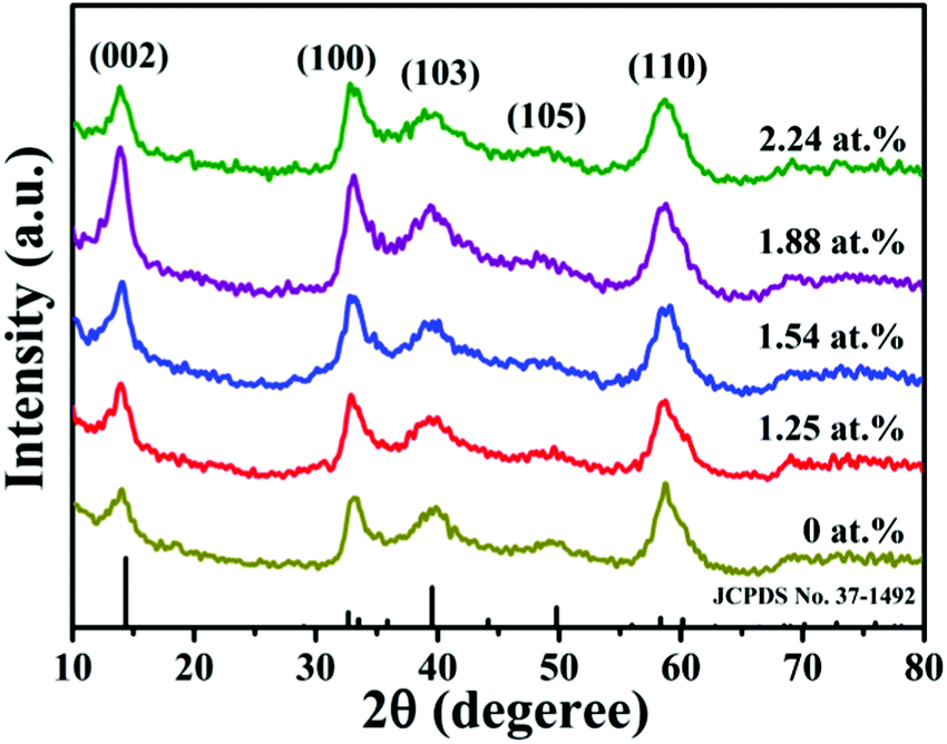 | ||
| Fig. 1 XRD patterns of the pristine MoS2 nanocrystals and the MoS2:Ho3+ nanocrystals. | ||
Fig. 2a shows the HRTEM image of the 1.54 at% MoS2:Ho3+ nanocrystals. It can be observed that the interplanar distance of the fringes is 0.22 nm which correspond well to the (103) plane of the hexagonal MoS2. The crystallite size is about 5 nm which is corresponding to the XRD results. The SAED image illustrates the polycrystalline structure of the MoS2:Ho3+ nanocrystals, as displayed in Fig. 2b. Five visible diffraction rings agree well with the (002), (100), (103), (105) and (110) planes of MoS2.
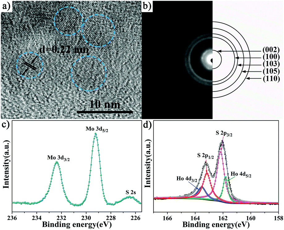 | ||
| Fig. 2 (a) HRTEM image, (b) SAED image, XPS spectra (c) high-resolution spectra for Mo 3d and (d) high-resolution spectra for S 2p and Ho 4d of the 1.54 at% MoS2:Ho3+ nanocrystals. | ||
To investigate the surface chemical composition and valance state, the corresponding XPS measurements of the 1.54 at% MoS2:Ho3+ nanocrystals are carried out. Fig. 2c illustrates the high-resolution Mo 3d XPS spectrum, the peaks at 232.38 eV and 229.22 eV can be ascribed to Mo 3d3/2 and Mo 3d5/2, which is characteristic of Mo4+ in MoS2.37 The high-resolution S 2p and Ho 4d spectra in Fig. 2d could be described as the four peaks located at 163.16 eV, 162.17 eV, 163.54 eV and 161.8 eV related to the S 2p1/2, S 2p3/2, Ho 4d3/2 and Ho 4d5/2 peaks, respectively.38,39 It can be assigned that the S ion is bivalent and the Ho ion is trivalent. Based on the above results, the Ho3+ ions have been successfully introduced into the MoS2 host crystal lattice.
Magnetic properties of the pristine MoS2 nanocrystals and the MoS2:Ho3+ nanocrystals with different doping concentrations have been studied using a VSM equipment. Fig. 3a shows the magnetization versus magnetic field (M–H) curves of the as-obtained samples with the magnetic field from −6 to 6 kOe at room temperature. Fig. 3b shows the amplified details of the curves. All of the MoS2:Ho3+ nanocrystals exhibit clear room temperature ferromagnetic (RTFM) behaviour and the pristine MoS2 nanocrystals exhibit non-magnetic character concluded from the nearly zero hysteresis loop. The saturation magnetizations (MS) are 0.013 emu g−1, 0.055 emu g−1, 0.037 emu g−1 and 0.033 emu g−1, of the as-synthesized samples with doping concentrations of 1.25 at%, 1.54 at%, 1.88 at% and 2.24 at%, respectively. From the inset of Fig. 3a, it can be obviously observed that the MS value increases as the doping concentration increases. The MS reaches the maximum when the doping concentration is 1.54 at% and then decreases. This behavior can be associated with the Bound Magnetic Polaron (BMP) model, considering that the BMPs are formed by the sp–df interaction between localized carriers and adjacent rare earth Ho3+ ions in the carrier orbits. According to the theory, it can produce more BMPs under increased doping concentration conditions, then BMPs begin to overlap, inducing a ferromagnetic interaction and an increase of MS. However, higher doping concentration decreases the average distance between adjacent Ho3+ ions, and the antiferromagnetic energy of Ho ions is lower than the ferromagnetic energy, and short range antiferromagnetic interactions may play a leading role and weak the ferromagnetism coupling, leading to a decrease in MS in the MoS2:Ho3+ nanocrystals.
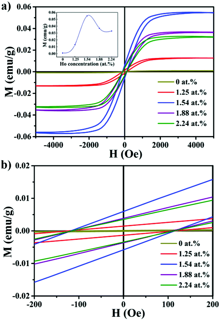 | ||
| Fig. 3 (a) M–H curves of the MoS2:Ho3+ nanocrystals with different doping concentrations taken at room temperature. The inset is the magnetic moment dependence on Ho concentration. (b) The enlarged view in the low field between −200 and 200 Oe. Clear hysteresis can be observed, indicating that the MoS2:Ho3+ nanocrystals are room-temperature ferromagnetic. | ||
For further investigation of the ferromagnetism of the 1.54 at% MoS2:Ho3+ nanocrystals, magnetization loops under different temperatures and the zero-field cooling (ZFC) and field cooling (FC) curves are measured by a SQUID. Fig. 4a shows the variation of the magnetization loops of the 1.54 at% MoS2:Ho3+ nanocrystals at 50 K, 150 K, 300 K and 330 K. The values of MS and HC are 0.2 emu g−1 and 215.9 Oe at 50 K, 0.08 emu g−1 and 45 Oe at 150 K, 0.06 emu g−1 and 30.9 Oe at 300 K, 0.058 emu g−1 and 28 Oe at 330 K, respectively. However, the magnetization loop is not saturated at a very high field at 50 K, and the positive magnetic susceptibility at low field with negative magnetic susceptibility at very high field indicates the coexistence of both the ferromagnetic and the diamagnetic characteristics of the as-synthesized materials at low temperature.
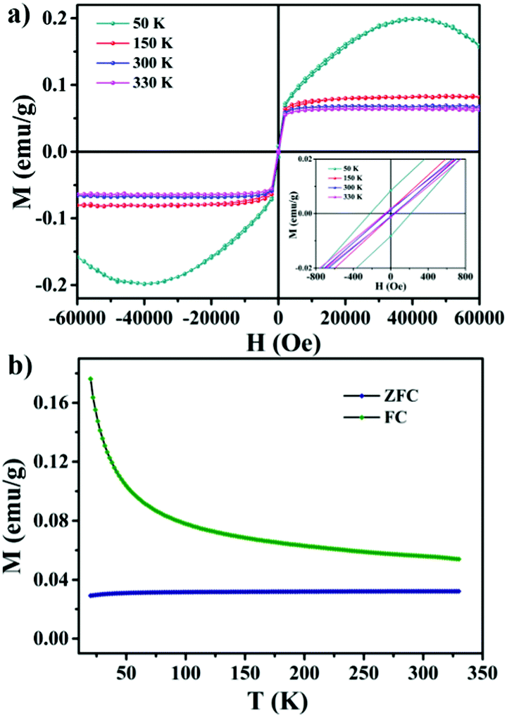 | ||
| Fig. 4 (a) M–H curves of the 1.54 at% MoS2:Ho3+ nanocrystals measured at 50 K, 150 K, 300 K and 330 K. The inset is the enlarged view in the low field between −800 and 800 Oe. (b) ZFC and FC M–T curves of the 1.54 at% MoS2:Ho3+ nanocrystals. All the results indicate that the samples are ferromagnetic at the range from 20 K to 300 K and the Curie temperature is above 300 K. | ||
The ZFC–FC curves in the temperature range of 20–330 K illustrate an apparent deviation, indicating that the existence of ferromagnetism in the whole temperature range and the Curie temperature of the as-synthesized samples is above 330 K. In addition, there is no blocking temperature in the cooling process, indicating that there are no ferromagnetic clusters in the nanocrystals. Therefore, the MoS2:Ho3+ nanocrystals can be regarded as the room temperature ferromagnetic material.
Based on the XRD and XPS results, it can be concluded that there is absence of the secondary phases in the MoS2 host material and doping has no significant effect on particles size. In addition, Cao et al. have reported that not only Mo vacancy but also S vacancy does not induce the magnetism.29 Therefore, the origin of the ferromagnetism of the Ho-doped MoS2 nanocrystals is attributed to the Ho dopant, excluding the effect on secondary phase, grain size and native defects of the samples.40–44 To further investigate the origin of room temperature ferromagnetism, first principles calculations have been performed using the VASP. First, to study the stability of the substitution or absorption models, the defect formation energy values of the models are calculated by the following equation:45
| Ef = Edefective − Epristine − n1μHo − n2μMo; |
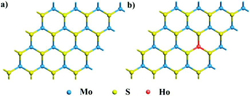 | ||
| Fig. 5 Top views of the slab models of (a) the pristine and (b) one Ho dopant defective MoS2 monolayers. Blue, yellow, and green balls stand for Mo, S, and Ho atoms, respectively. | ||
To further study the magnetism of the MoS2:Ho3+ nanocrystals, the total density of states (TDOS) are calculated as shown in Fig. 6. The TDOS of the Mo16S32 (Fig. 6a) shows the perfect symmetry, indicating the nonmagnetic semiconductor property of the pristine Mo16S32 with the zero magnetic moment. From Fig. 6b, it can be observed that the TDOS of the Mo15Ho1S32 is asymmetric near the Fermi level, indicating that the Ho doped MoS2 system is spin polarized. The calculated overall magnetic moment is 1.839 μB. Furthermore, the details of the magnetic moment of every atom are presented in the ESI.† The narrowed band gap is attributed to the increased electrons induced by Ho doping.
 | ||
| Fig. 6 The total density of states (TDOS) of (a) the Mo16S32 slab model and (b) the Mo15Ho1S32 slab model. The dashed line indicates the Fermi level. | ||
The partial densities of states (PDOS) of the nearest neighbouring Mo1 atoms around the Ho atom, the next nearest neighbouring Mo2 atoms around the Ho atom and the S atoms and the Ho atom in the Mo15Ho1S32 slab model are shown in Fig. 7. The 4d orbital of Mo is notably overlapped with the 3p orbital of S and the 4f orbital of Ho near the Fermi level, indicating the strong hybrid effect of the electrons on these orbitals. In the Ho doped structure, the magnetic moments of the nearest neighbouring Mo1 atoms and the next nearest neighbouring Mo2 atoms around the Ho atom are 5.815 μB and −4.35 μB, respectively. In addition, the S atoms make a little contribution to the total magnetic moment (1.103 μB). It can be concluded from the above results that the ferromagnetism mainly comes from the strong hybridization among the Mo 4d, S 3p and Ho 4f orbitals in the Ho doped MoS2 system. Fig. 8 illustrates the spin density of the Mo15Ho1S32 slab model. It can be observed that spin polarized states are primarily localized at the nearest neighbouring Mo atoms around the Ho atom, which can induce the ferromagnetic order.
 | ||
| Fig. 7 The partial density of states (PDOS) of (a) the nearest Mo1 atoms, (b) the next nearest Mo2 atoms, (c) the S atoms and (d) the Ho atom of the Mo15Ho1S32 slab model. | ||
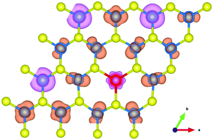 | ||
| Fig. 8 Spin density of the Mo15Ho1S32 monolayer. The orange and pink distributions correspond to the positive (spin up) and negative (spin down) values, respectively. The isosurface value is 0.02 e Å−3. | ||
4 Conclusions
In summary, the pristine MoS2 nanocrystals and the MoS2:Ho3+ nanocrystals have been successfully obtained by a simple gas–liquid phase chemical deposition method and the as-obtained MoS2:Ho3+ nanocrystals exhibit robust room-ferromagnetism with a maximum magnetic moment of 0.055 emu g−1. More importantly, the ferromagnetism can be tuned by changing the Ho doping concentrations. From the results of first-principles calculations, the ferromagnetism is primarily induced by Ho doping. This work indicates that doping of rare earth elements can be an excellent method for engineering and manipulating the magnetic properties of TMDs.Conflicts of interest
There are no conflicts to declare.Acknowledgements
This work was funded by the National Natural Science Foundation of China, No. 11474124 and 61674065 and Project 2017110 Supported by Graduate Innovation Fund of Jilin University. The calculations in our work are supported by the High Performance Computing Centre of Jilin University, China.Notes and references
- T. Dietl, Nat. Mater., 2010, 9, 965 CrossRef CAS PubMed.
- D. Pesin and A. H. MacDonald, Nat. Mater., 2012, 11, 409 CrossRef CAS.
- T. Dietl and H. Ohno, Rev. Mod. Phys., 2014, 86, 187–251 CrossRef CAS.
- D. D. Wang, Q. Chen, G. Z. Xing, J. B. Yi, S. R. Bakaul, J. Ding, J. L. Wang and T. Wu, Nano Lett., 2012, 12, 3994–4000 CrossRef CAS.
- A. Goktas, F. Aslan, B. Yeşilata and İ. Boz, Mater. Sci. Semicond. Process., 2018, 75, 221–233 CrossRef CAS.
- M. Saleem, S. A. Siddiqi, S. Atiq, M. S. Anwar, I. Hussain and S. Alam, Mater. Charact., 2011, 62, 1102–1107 CrossRef CAS.
- H. Atsufumi and T. Koki, J. Phys. D: Appl. Phys., 2014, 47, 193001 CrossRef.
- L. Z. Li, R. Qin, H. Li, L. L. Yu, Q. H. Liu, G. F. Luo, Z. X. Gao and J. Lu, ACS Nano, 2011, 5, 2601–2610 CrossRef CAS.
- Q. Lu, Q. Zhao, T. Y. Yang, C. B. Zhai, D. X. Wang and M. Z. Zhang, ACS Appl. Mater. Interfaces, 2018, 10, 12947–12953 CrossRef CAS PubMed.
- Y. Kang, Q. Leng, D. L. Guo, D. Z. Yang, Y. P. Pu and C. G. Hu, Nano-Micro Lett., 2016, 8, 13–19 CrossRef.
- K. F. Mak and J. Shan, Nat. Photonics, 2016, 10, 216 CrossRef CAS.
- S. Das, A. Prakash, R. Salazar and J. Appenzeller, ACS Nano, 2014, 8, 1681–1689 CrossRef CAS PubMed.
- T. Ritschel, J. Trinckauf, K. Koepernik, B. Büchner, M. v. Zimmermann, H. Berger, Y. I. Joe, P. Abbamonte and J. Geck, Nat. Phys., 2015, 11, 328 Search PubMed.
- Z. Li, C. Liu, X. Zhang, J. Guo, X. Zhang and W. Guo, J. Phys. Chem. C, 2018, 122, 207–215 CrossRef CAS.
- G. U. Siddiqui, M. Sajid, J. Ali, S. W. Kim, Y. H. Doh and K. H. Choi, Sens. Actuators, B, 2018, 266, 354–363 CrossRef.
- X. Y. Shi, S. Posysaev, M. Huttula, V. Pankratov, J. Hoszowska, J. C. Dousse, F. Zeeshan, Y. R. Niu, A. Zakharov, T. H. Li, O. Miroshnichenko, M. Zhang, X. Wang, Z. J. Huang, S. Saukko, D. L. González, S. V. Dijken, M. Alatalo and W. Cao, Small, 2018, 14, 1704526 CrossRef.
- W. Lee, Y. Liu, Y. J. Lee, B. K. Sharma, S. M. Shinde, S. D. Kim, K. Nan, Z. Yan, M. D. Han, Y. G. Huang, Y. H. Zhang, J. H. Ahn and J. A. Rogers, Nat. Commun., 2018, 9, 1417 CrossRef.
- M. Amani, M. L. Chin, A. G. Birdwell, T. P. O’Regan, S. Najmaei, Z. Liu, P. M. Ajayan, J. Lou and M. Dubey, Appl. Phys. Lett., 2013, 102, 193107 CrossRef.
- J. F. Xie, H. Zhang, S. Li, R. X. Wang, X. Sun, M. Zhou, J. F. Zhou, X. W. Lou Xiong and Y. Xie, Adv. Mater., 2013, 25, 5807–5813 CrossRef CAS.
- M. Donarelli, S. Prezioso, F. Perrozzi, F. Bisti, M. Nardone, L. Giancaterini, C. Cantalini and L. Ottaviano, Sens. Actuators, B, 2015, 207, 602–613 CrossRef CAS.
- M. A. Lukowski, A. S. Daniel, F. Meng, A. Forticaux, L. Li and S. Jin, J. Am. Chem. Soc., 2013, 135, 10274–10277 CrossRef CAS.
- A. Ramasubramaniam and D. Naveh, Phys. Rev. B: Condens. Matter Mater. Phys., 2013, 87, 195201 CrossRef.
- A. L. Li, J. L. Pan, Z. X. Yang, L. Zhou, X. Xiong and F. P. Ouyang, J. Magn. Magn. Mater., 2018, 451, 520–525 CrossRef CAS.
- J. Pan, R. Wang, X. Y. Zhou, J. S. Zhong, X. Y. Xu and J. G. Hu, Phys. Chem. Chem. Phys., 2017, 19, 24594–24604 RSC.
- M. Luo, Y. E. Xu and Y. H. Shen, J. Supercond. Novel Magn., 2017, 30, 2849–2854 CrossRef CAS.
- A. Majid, A. Imtiaz and M. Yoshiya, J. Appl. Phys., 2016, 120, 142124 CrossRef.
- Y. C. Cheng, Z. Y. Zhu, W. B. Mi, Z. B. Guo and U. Schwingenschlögl, Phys. Rev. B: Condens. Matter Mater. Phys., 2013, 87, 100401 CrossRef.
- A.-M. Hu, L.-l. Wang, W.-Z. Xiao, G. Xiao and Q.-Y. Rong, Comput. Mater. Sci., 2015, 107, 72–78 CrossRef CAS.
- D. Cao, H. B. Shu, T. Q. Wu, Z. T. Jiang, Z. W. Jiao, M. Q. Cai and W. Y. Hu, Appl. Surf. Sci., 2016, 361, 199–205 CrossRef CAS.
- H. Tan, W. Hu, C. Wang, C. Ma, H. L. Duan, W. S. Yan, L. Cai, P. Guo, Z. H. Sun, Q. H. Liu, X. S. Zheng, F. C. Hu and S. Q. Wei, Small, 2017, 13, 1701389 CrossRef.
- G. C. Xu, X. S. Wang, Y. P. Sun, X. Chen, J. Y. Zheng, L. F. Sun, L. Y. Jiao and J. H. Li, Nano Res., 2015, 8, 2946–2953 CrossRef CAS.
- P. Wang, T. Y. Yang, R. Zhao and M. Z. Zhang, Phys. Chem. Chem. Phys., 2016, 18, 10123–10128 RSC.
- R. Zhao, P. Wang, T. Y. Yang, Z. F. Li, B. X. Xiao and M. Z. Zhang, J. Phys. Chem. C, 2015, 119, 28679–28684 CrossRef CAS.
- G. Kresse and J. Furthmüller, Phys. Rev. B: Condens. Matter Mater. Phys., 1996, 54, 11169–11186 CrossRef CAS.
- G. Kresse and D. Joubert, Phys. Rev. B: Condens. Matter Mater. Phys., 1999, 59, 1758–1775 CrossRef CAS.
- J. P. Perdew, K. Burke and M. Ernzerhof, Phys. Rev. Lett., 1996, 77, 3865–3868 CrossRef CAS.
- L. N. Wang, Y. Ma, M. Yang and Y. X. Qi, Electrochim. Acta, 2015, 186, 391–396 CrossRef CAS.
- G. L. Kabongo, P. S. Mbule, G. H. Mhlongo, B. M. Mothudi, K. T. Hillie and M. S. Dhlamini, Nanoscale Res. Lett., 2016, 11, 418 CrossRef.
- W. Xiao, W. J. Zhou, T. Feng, Y. H. Zhang, H. D. Liu and L. L. Tian, Materials, 2016, 9, 783 CrossRef.
- A. Goktas, Appl. Surf. Sci., 2015, 340, 151–159 CrossRef CAS.
- S. Sambasivam, D. P. Joseph, D. R. Reddy, B. K. Reddy and C. K. Jayasankar, Mater. Sci. Eng., B, 2008, 150, 125–129 CrossRef CAS.
- A. Goktas, J. Alloys Compd., 2018, 735, 2038–2045 CrossRef CAS.
- A. Goktas and İ. H. Mutlu, J. Electron. Mater., 2016, 45, 5709–5720 CrossRef CAS.
- M. El-Hagary, M. Emam-Ismail, E. R. Shaaban, A. Al-Rashidi and S. Althoyaib, Mater. Chem. Phys., 2012, 132, 581–590 CrossRef CAS.
- P. J. Zhao, J. M. Zheng, P. Guo, Z. Y. Jiang, L. K. Cao and Y. Wan, Comput. Mater. Sci., 2017, 128, 287–293 CrossRef CAS.
Footnote |
| † Electronic supplementary information (ESI) available: The EDS of the Ho doped MoS2 nanocrystals and the atomic structures of the 4 × 4 × 1 MoS2 supercells of S-top and HC. See DOI: 10.1039/c8cp05790g |
| This journal is © the Owner Societies 2019 |