
Interplay of orbital hopping and perpendicular magnetic field in anisotropic phase transitions for Bernal bilayer graphene and hexagonal boron-nitride
P.
T. T. Le
*ab,
M.
Davoudiniya
 c and
M.
Yarmohammadi
*d
c and
M.
Yarmohammadi
*d
aTheoretical Physics Research Group, Advanced Institute of Materials Science, Ton Duc Thang University, Ho Chi Minh City, Vietnam. E-mail: lethithuphuong@tdtu.edu.vn
bFaculty of Applied Sciences, Ton Duc Thang University, Ho Chi Minh City, Vietnam
cDepartment of Energy Engineering and Physics, Amirkabir University of Technology, 14588 Tehran, Iran
dLehrstuhl für Theoretische Physik I, Technische Universität Dortmund, Otto-Hahn Straße 4, 44221 Dortmund, Germany. E-mail: mohsen.yarmohammadi@tu-dortmund.de
First published on 16th November 2018
Abstract
We theoretically address the perpendicular magnetic field effects on the electronic phase of Bernal bilayer graphene and hexagonal boron-nitride (h-BN) taking into account the total and orbital-projected electronic bands using the tight-binding parameters in the Harrison model, followed by the Green's function method. First, we confirm that our model is computationally efficient and accurate for calculating the magneto-orbital electronic phase transition by reproducing the semimetallic and insulating treatments of pristine Bernal bilayer graphene and h-BN, respectively. In our model, the magnetic field couples only to the electron spin degrees of freedom (with the same contributions for spin-up and spin-down) due to the low dimension of the systems. Here, the main features of the phase transitions are characterized by the electronic density of states (DOS). We found that sp2-hybridization is destroyed when the systems are immersed in the magnetic field, leading to a phase transition to metal for both systems at strong magnetic fields. While there is no phase transition for bilayer graphene at weak magnetic fields, for the case of bilayer h-BN, an insulator to semiconductor phase transition can be viewed, making h-BN more applicable in industry. In bilayer graphene, the anisotropic phase transition appears as insulator–semiconductor, insulator–metal, and semimetal–metal for s-, {px + py}-, and pz-orbitals, respectively, whereas in the case of bilayer h-BN, one observes the same transitions for {s,pz}-orbitals but insulator–semiconductor for {px + py} orbitals. Generically, our findings highlight that the applied magnetic field manipulates the band structure of bilayer graphene and h-BN, and gives ideas to experimentalists for tuning the electro-optical properties of these materials.
1 Introduction
Graphene is a two-dimensional (2D) material of carbon (C) atoms packed in a planar hexagonal lattice with sp2-hybridization forming strong in-plane (σ) and weak out-of-plane (π) bonds.1 While the π bonds only consist of pz orbitals because of the atomic number of carbon, the in-plane σ bonds include s, px, and py orbitals.1,2 Graphene as a prominent material has many unusual properties to open up new horizons for possible applications in electronic devices.3,4 The electronic band structure of graphene leads to the Dirac equation for massless fermions with a speed of c/300 in which c is the speed of light.5,6Bilayer graphene plays a key role in practical applications and it can be formed by stacking graphene monolayers on top of each other. Bernal stacking as the most stable stacking of bilayer graphene (the reason why we will focus on this type of stacking) is one of the layered graphene systems with two atoms (A and B) per unit cell in one layer (Fig. 1). In this structure, one of the atoms of the first layer is located directly in the center of the honeycomb lattice of the second layer.7 Monolayer graphene has a linear dispersion energy while bilayer graphene has a quadratic spectrum which attenuates the Klein tunneling paradox in monolayer graphene which restricts its applications.8–10
 | ||
Fig. 1 The geometry of Bernal bilayer 2D lattices. Each unit cell (blue rectangle) includes four atoms. For bilayer graphene {A1, A2, B1, B2} ≡ carbon atom, while in bilayer h-BN, {A1, A2} ≡ boron and {B1, B2} ≡ nitrogen. The intralayer and interlayer hopping energies are labelled by t and t′, respectively. The perpendicular magnetic field is also applied in the z-direction as ![[B with combining right harpoon above (vector)]](https://www.rsc.org/images/entities/i_char_0042_20d1.gif) = hêz where êz is the unit vector along the z-direction. = hêz where êz is the unit vector along the z-direction. | ||
Another significant compound in new nanoelectronic devices is hexagonal boron-nitride (h-BN) which is a 2D insulator lattice.11 This compound has drawn a great deal of attention and has been applied for a variety of real applications in industry such as for surface coatings and ceramic composites because of its unique properties including large thermal conductivity, excellent lubricity, and chemical inertness.12 In the h-BN structure, boron and nitrogen atoms are bonded compartmentally by sp2-hybridization.13 In contrast to bilayer graphene, bilayer h-BN has a wide energy gap because of the difference between the electronegativities of the boron and nitrogen atoms.14,15
Recently there have been several papers that have studied the effect of the parallel magnetic field (B‖) on bilayer graphene.16,17 In 2D infinite materials with zero thickness, the particle in-plane motion is unaffected by B‖ and only out-of-plane motion can be changed, while in quasi-2D systems with a finite width, B‖ can also affect the in-plane motion. However, in the absence of thickness of materials, B‖ only couples to the particle spin, forming a magnetic ordering of carriers.18–20 One of the interesting findings in the investigation of magnetic field effects on the electronic properties of low-dimensional materials like carbon and BN nanotubes is the reduction of band gap size in gapped structures21 which will be confirmed in our results too. However, to the best of our knowledge, the magneto-orbital electronic phase transitions in bilayer graphene and h-BN have not been well studied theoretically to date.
To study the effect of the perpendicular magnetic field on the electronic phase of Bernal bilayer graphene and BN, we use the Green's function technique, followed by the Harrison model, i.e. the orbital version of the tight-binding model. It is necessary to mention that different stackings of bilayer graphene or h-BN would be explored in the same manner.22 The key findings are as follows. At zero magnetic field, both total and partial DOS have a certain electronic phase. A perpendicular magnetic field changes the electronic states of the systems to a combination of partial flat bands, originating from destroying the subbands, resulting in anisotropic orbital phase transitions between π- and σ-states.
The present paper is organized as follows. In Section 2, we formulate our model Hamiltonian and compute the Green's function. Then, we calculate total and partial DOS of the aforementioned systems based on the derived Green's function. In Section 3, we show the numerical results, discuss, and analyze the total and orbital contributions of each system in the presence of a magnetic field. Finally, in Section 4, we conclude and summarize our main results.
2 Model description and electronic density of states
The intent of this section is to introduce the model addressing the bilayer 2D lattices to allow for a systematic and routine assessment of anisotropic electronic phase transition. To describe the dynamics of Dirac fermions in the above-mentioned Bernal bilayer graphene and h-BN in the presence of a magnetic field, the following tight-binding Harrison model Hamiltonian has been used.23 These systems have similar structures (honeycomb lattices) due to their alike hybridization in-plane bonding. For this reason, this model can even be used for other cases, | (1) |
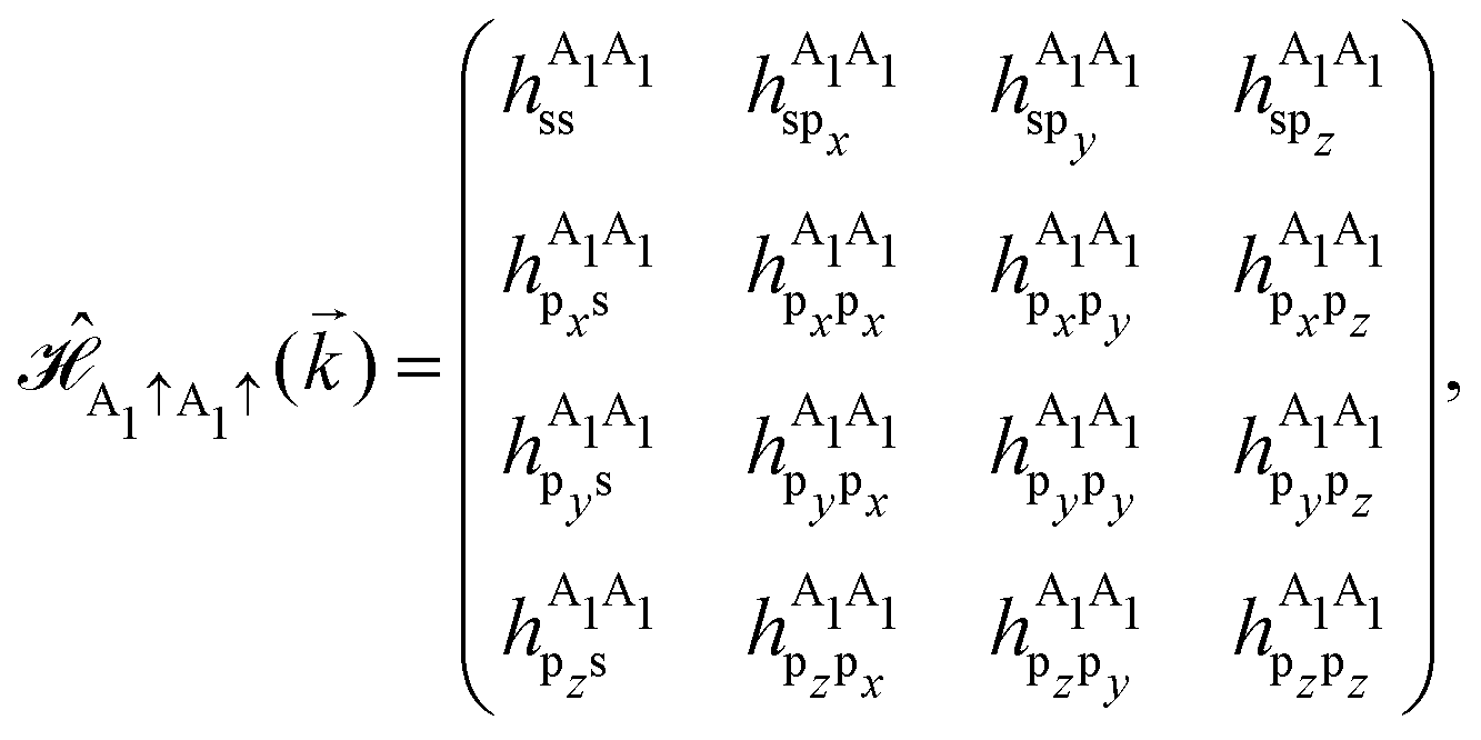
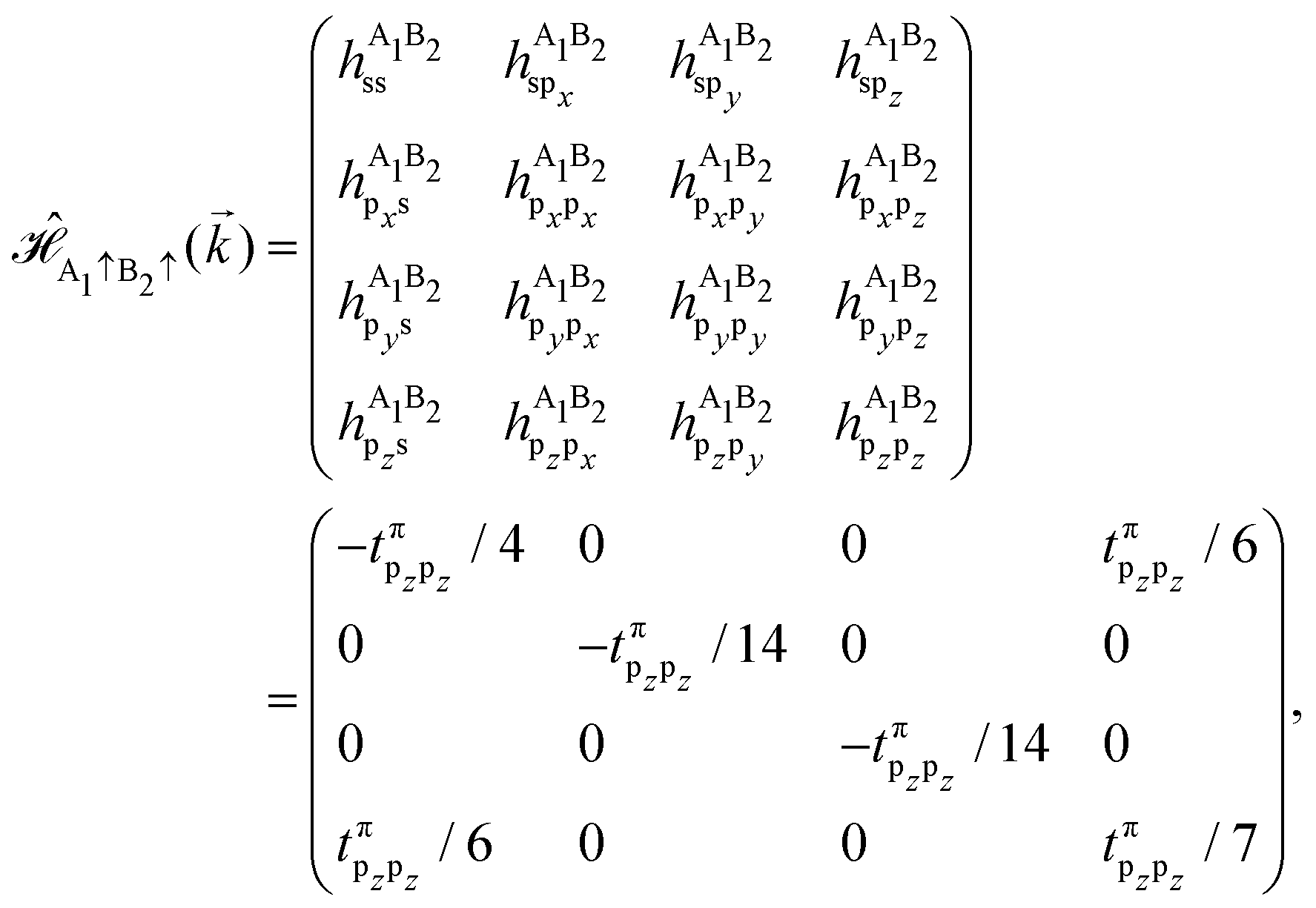
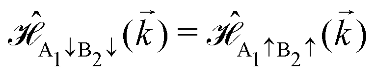
 defines the hopping integral between an electron with spin σ from μ orbital of subsite α in the unit cell i to another electron with spin σ′ from ν orbital of subsite β in the unit cell j. εασiμ is the on-site energy for an electron with spin σ from subsite α of μ orbital in the unit cell i. Also, 1 and 2 are used for top and bottom layers. Since our structures are considered as bilayers including four atoms per unit cell [A1, B1, A2, and B2] as illustrated in Fig. 1, by considering four orbitals for each atom and spin-up and spin-down for each electron, the Hamiltonian can be presented by a 32 × 32 matrix
 | (2) |
 is given by
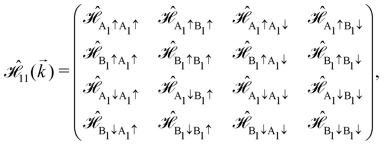 | (3) |
 is also described by
 | (4) |
Also,  where a, b = {A1(2),B1(2)}. On the other hand,
  . It is necessary to mention that the distances between two layers of bilayer graphene and h-BN have been considered to be 3.35 Å and 3.17 Å, respectively.24–26 The tabular forms of
  are given by
 | (5) |
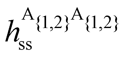
In our calculations, we have used the reported values from ref. 27–30 by setting all physical constants equal to one. Also, the on-site energy of the p orbitals is considered as the origin of energy. As a remarkable point, the sign of on-site energy for s orbitals is negative while for p orbitals it can be negative or positive.23,27,31,32 The non-zero elements of (5) are listed in Table 1, and other elements are zero. Also, the general form of  reads
reads
 | (6) |
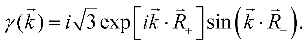
ε(![[k with combining right harpoon above (vector)]](https://www.rsc.org/images/entities/i_char_006b_20d1.gif) ) = exp[i· ) = exp[i·![[R with combining right harpoon above (vector)]](https://www.rsc.org/images/entities/i_char_0052_20d1.gif) +]cos(·−), +]cos(·−), | (7a) |
 | (7b) |
± = (![[a with combining right harpoon above (vector)]](https://www.rsc.org/images/entities/i_char_0061_20d1.gif) 1 ± 2)/2 and the primitive unit cell vectors of the honeycomb lattice are
1 ± 2)/2 and the primitive unit cell vectors of the honeycomb lattice are  and
and  . The inter-atomic distances are given by aCC0 ≃ 1.4 Å and aBN0 ≃ 1.9 Å where êx and êy are the unit vectors along the x- and y-direction, respectively.
| Element | Carbon | Boron | Nitrogen |
|---|---|---|---|
|
−8.453 | −3.570 | −14.070 |
|
+4.346 | +2.320 | +2.470 |
 is the hopping energy for normalization in our calculations
| Element | Value | Element | Value |
|---|---|---|---|
|
−6.769[1 + 2ε()] |

|
+5.580γ() |

|
−6.769[1 + ε()] |

|
+4.035γ() |

|
−5.580γ() |

|
−6.039ε() + 3.033 |

|
0 |
|
0 |

|
+5.580[1 + ε()] |

|
0 |

|
2.031ε() − 5.037 |
|
0 |

|
+4.035γ() |

|
0 |

|
0 |

|

|
Finally, we have  [Î being the identity matrix] and
  [
[![[0 with combining circumflex]](https://www.rsc.org/images/entities/char_0030_0302.gif) being the zero matrix] where h = gμBB is the applied external magnetic field strength which couples only to the electron spin, μB is the Bohr magneton, and g is the degeneracy number. For the
being the zero matrix] where h = gμBB is the applied external magnetic field strength which couples only to the electron spin, μB is the Bohr magneton, and g is the degeneracy number. For the  part:
part:
 | (8) |
 . Also,
  and other elements get zero values. It is worthwhile mentioning that in addition to the magnetic field, the electric field can also tune the electronic properties of bilayer 2D materials like graphene, gapped graphene-like structures, and phosphorene.33–36 For instance, in our recent work,36 it has been shown that the electric field and dilute charged impurities effectively affect the electronic phase of Bernal bilayer phosphorene.
By using eqn (2), the explicit form of Green's function matrix can be found by the following relation37
 | (9) |
DOS can be calculated by tracing over the imaginary part of diagonal Green's function elements. By setting iωn → ![[scr E, script letter E]](https://www.rsc.org/images/entities/char_e140.gif) + i0+ as a numerical calculation in which 0+ = 10 meV is a very small real number, total and partial DOS can be calculated by, respectively,
+ i0+ as a numerical calculation in which 0+ = 10 meV is a very small real number, total and partial DOS can be calculated by, respectively,
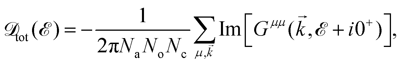 | (10a) |
 | (10b) |
is taken over the honeycomb reciprocal space, i.e. the first Brillouin zone. The study of DOS in bilayer graphene and h-BN constitutes the main aim in this work. In the next section, the results are presented. In the following plots, the hopping parameter 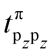 between pz-orbitals is renamed to t.
3 Numerical results and discussion
In what follows, a proper interpretation of our main outcomes is presented for the numerically calculated electronic DOS of magnetic-field-induced bilayer Bernal graphene and h-BN. Generically, we divide the section into two parts. First, we plot total and partial DOS of both pristine systems as a function of energy spectrum in units of t within the range [−10, +6] eV in Fig. 2. Second, the effect of magnetic field is studied on the total and partial DOS of systems separately in the vicinity of the Fermi energy level, i.e. /t ≃ 0, in Fig. 3 and 5 and Fig. 4 and 6 within the energy range [−3, +3] eV, respectively. We stress that the anisotropic electronic phase transitions stemming from the extrinsic perpendicular magnetic field appear in the case of various behaviors of the partial DOS around the Fermi energy level. The insulating/semiconducting and metallic/semimetallic treatment of systems is characterized by the zero and no-zero DOS at /t ≃ 0, respectively. It should be noted that in the present work, it is assumed that the systems are optimized before and after applying the magnetic field. Additionally, it is worth noting that the partial DOS for each orbital is plotted according to the sum of all those orbitals in the bilayer not the sublattice orbitals separately. We stress that unless otherwise stated explicitly, the constants ħ = kB = g = μB = e = me = 1 are used throughout the paper in numerical calculations for simplicity. By this, one can determine the values of the magnetic field in terms of the Tesla, for example, for the value h/t = 0.1 we have a magnetic field ![[scr B, script letter B]](https://www.rsc.org/images/entities/char_e13f.gif) ≃ 0.3 T.
≃ 0.3 T.
 | ||
| Fig. 2 Calculated TDOS and OPDOS of pristine Bernal bilayer (a) graphene and (b) h-BN. | ||
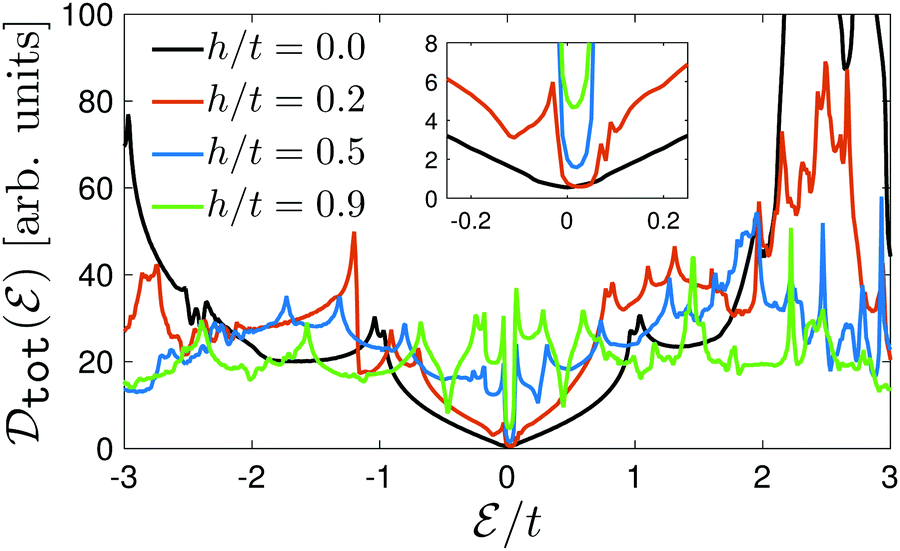 | ||
| Fig. 3 Calculated TDOS of magnetic field-induced Bernal bilayer graphene. | ||
 | ||
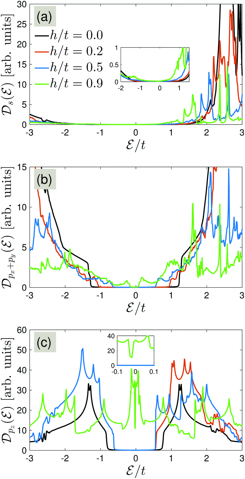
| Fig. 4 Calculated DOS of magnetic field-induced Bernal bilayer graphene for (a) s-orbitals, (b) {px + py}-orbitals, and (c) pz-orbitals. | ||
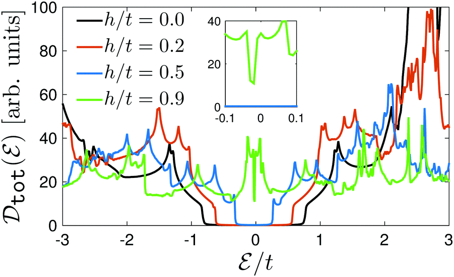 | ||
| Fig. 5 Calculated TDOS of magnetic field-induced Bernal bilayer h-BN. | ||
 | ||
| Fig. 6 Calculated DOS of magnetic field-induced Bernal bilayer h-BN for (a) s-orbitals, (b) {px + py}-orbitals, and (c) pz-orbitals. | ||
3.1 Without a magnetic field
Fig. 2(a) shows the total DOS (TDOS) and the orbital-projected DOS (OPDOS) plots as a function of energy/t for the graphene bilayer when the magnetic field is absent. Actually, we find how different orbitals of carbon atoms contribute to the electronic states. It can be observed that the TDOS of bilayer Bernal graphene exhibits multiple van Hove singularities over the entire energy range from −10 eV to +6 eV, which is consistent with the TDOS obtained in ref. 38–40. Also, TDOS is very small at the valence bands compared to at the conduction bands, which originates from the shape of the bands. Viewed from OPDOS, both π-orbitals (pz-orbitals) and σ-orbitals ({s,px + py}-orbitals) have contributions in the states far from the Fermi level more than near energies. The valence bands between −10 eV and −3 eV have small contributions from π-orbitals and the main contributions stem from σ-orbitals, while the conduction bands higher than +3 eV are only from σ-orbitals.
However, in the vicinity of the Fermi level, i.e. low-energy side /t ∈ [−3, +3], the contribution from the π states of carbon atoms to the TDOS is much higher than that from the σ states. The fact that pz-orbitals are always dominant in low-dimensional flat systems due having to more degrees of freedom can be confirmed here. Thus, it can be considered that the semimetallic treatment of Bernal bilayer graphene is mainly from π-orbitals. It should be pointed out that these results have been produced/reported already in numerous works, but few theoretical investigations beyond the low-energy limit, first-principle calculations, and experiments have been found to date. We stress again that this first part is only to confirm our model to allow for a suitable study on magnetic field effects. Briefly, the orbital electronic phase of states is the insulating phase for {s,px + py}-orbitals and the semimetallic phase for pz orbitals.
As for the case of Bernal bilayer h-BN, the evolution of TDOS and OPDOS of the electronic states is analyzed in Fig. 2(b). We observe that bilayer h-BN is an insulator with a band gap around 4.57 eV [≃1.5t], in agreement with ref. 41 and 42. The contribution of the π- and σ-orbitals are precisely the same as in case of bilayer graphene, as expected. Contrary to bilayer graphene, all orbital electronic phases are in the insulating phase. We expect that the Zeeman splitting effect stemming from the applied perpendicular magnetic field can change the band gap and phase of electronic states systematically due to the different nature of bands in the presence of perturbations.
3.2 With a magnetic field
Now let see how the interplay of the hopping parameters of both systems and the magnetic field affect the orbital phases of atoms. To this end, we consider the same parameters as in Fig. 2 but in the presence of a magnetic field. Since the applied magnetic field is a Zeeman field, spin splitting is expected. However, in the present model, the contribution of both spin-up and spin-down is the same in numerical computations, originating from the almost flat structure of each layer of bilayer graphene. In fact, all spin states are in the same level when dealing with 2D flat geometries of atoms. For this reason, there is no separated DOS for spin-up and spin-down. Another reason that we didn't model spin in the effective Hamiltonian operator comes from our interest in the electronic properties, especially the electronic phases, not the magnetic ones. Of course, this can be studied as well in our future research. For instance, for simplicity, one can model the magnetic field with different signs for couplings with different spins.In Fig. 3 we show the TDOS of Bernal bilayer graphene associated with different perpendicular magnetic fields as a function of the normalized energy /t. As depicted in Fig. 3, the TDOS exhibits many peaks when the system is immersed in the magnetic field, and the number of these pronounced peaks depends strongly on the magnetic field strength. This can be understood better from the Landau levels (LLs) which appear when a magnetic field is present.43–45 We do not study LLs here. The observed peaks corresponding to LLs that are prominent for electronic transport properties lead in turn to an electronic phase transition from semimetal to metal, stemming from larger non-zero DOS around the Fermi energy level. Actually, the initial distribution of electronic waves is destroyed (sp2-hybridization) when electrons spin interact with the magnetic field. In other words, the magnetic field efforts in rotating and/or flipping the host spins leads to this destruction. Thus, the electronic states are suppressed, resulting in a new wave configuration. From this point, an increase of DOS at /t = 0 in the magnetic field can be expected and/or viewed. The increase trend also comes from the rule that the area under the DOS should be conserved. Decreasing the peaks at the high-energy side causes an increase in the low-energy side in order to conserve the area under DOS curves at different magnetic fields. It should be noted that the new hybridization can be found by first-principles calculations, which is out of the scope of the present paper.
Now we proceed with the OPDOS of bilayer graphene in Fig. 4 to see how in-plane and out-of-plane orbitals contribute in the mentioned electronic phase transition in the TDOS. The following anisotropic electronic phase transition between π- and σ-orbitals is an interesting issue. To clearly show these transitions, we plot DOS of s-, {px + py}-, and pz-orbitals separately in panels (a), (b), and (c), respectively. Obviously, there is no contribution from s-orbitals in the semimetal–metal phase transition of magnetic field-induced bilayer graphene and most contribution comes from {px + py}- and pz-orbitals. The characteristic decreasing band gap of s-orbitals with perpendicular magnetic field is shown in the inset panel of Fig. 4(a), leading to an insulator–semiconductor phase transition. Raising the magnetic field (h) is expected to destroy the spherical symmetry of s-orbitals, and thus the electronic wave distribution should change. This magnetic field induces a scattering process to the host electrons with higher momentum ![[q with combining right harpoon above (vector)]](https://www.rsc.org/images/entities/i_char_0071_20d1.gif) transfer, leading to different propagation direction and eventually a different phase. Additionally, {px + py}-orbital distribution resulting from the application of the magnetic field indicates that strong interactions between host spins and the magnetic field highly affect the phase of these states. With magnetic field, it is observed that the band gap decreases, resulting in an insulator–semiconductor phase transition at weak magnetic fields and an insulator–metal phase transition at strong ones, as shown in Fig. 4(b). This is what we call “anisotropic” phase transition. Both s- and {px + py}-orbitals are in-plane states but s-orbitals show the insulator–semiconductor phase transition at strong magnetic fields, whereas {px + py}-orbitals demonstrate an insulator–semiconductor and insulator–metal phase transition for weak and strong magnetic fields, respectively.
transfer, leading to different propagation direction and eventually a different phase. Additionally, {px + py}-orbital distribution resulting from the application of the magnetic field indicates that strong interactions between host spins and the magnetic field highly affect the phase of these states. With magnetic field, it is observed that the band gap decreases, resulting in an insulator–semiconductor phase transition at weak magnetic fields and an insulator–metal phase transition at strong ones, as shown in Fig. 4(b). This is what we call “anisotropic” phase transition. Both s- and {px + py}-orbitals are in-plane states but s-orbitals show the insulator–semiconductor phase transition at strong magnetic fields, whereas {px + py}-orbitals demonstrate an insulator–semiconductor and insulator–metal phase transition for weak and strong magnetic fields, respectively.
As for pz-orbitals, when bilayer graphene is subjected to an external magnetic field, the distribution of electronic waves around the Fermi level is influenced and a semimetal–metal phase transition appears, as portrayed in Fig. 4(c). Then, one concludes that the total semimetal–metal phase transition of magnetic field-induced bilayer graphene stems from the contribution of pz states much more than from other orbitals. Concisely, we have an insulator–semiconductor, insulator–metal, and semimetal–metal phase transition for s-, {px + py}-, and pz-orbitals, respectively. The increase of DOS at /t = 0 under the application of a perpendicular magnetic field highlights that the applied magnetic field manipulates the band structure, as reported in ref. 46–49.
Obviously, increasing the applicability of bilayer 2D systems in the semiconductor industry requires having a semiconductor analogue of Bernal bilayer graphene. In this work, we focus on only one of them, Bernal bilayer h-BN and mention only in passing that our methodological advancements now allow us to accurately and efficiently tune the electronic phase of bilayer h-BN from theory. In principle, it is now possible to use our confirmed model to also account for other gapped Bernal bilayer 2D materials, which are of particular importance in materials science. To this end, we plot Fig. 5 to show the effect of perpendicular magnetic field on TDOS of bilayer h-BN. Please note that only a concise discussion of the bilayer h-BN is possible in these last paragraphs because most of the analysis is the same as in the case of graphene mentioned above. The central concept in Fig. 5 is the insulator–semiconductor phase transition at weak magnetic fields, while the insulator–metal transition occurs at strong ones. However, the electronic wave distribution in the presence of a magnetic field again shows different phases due to the subbands which appear due to the magnetic field (originating from LLs). Since in the case of h-BN the different electronegativities of boron and nitrogen create on-site scattering mechanisms, one expects that the magnetic field destroys the midgap states, leading to a reduction of the band gap and consequently the phase transition.
For the purpose of this work, we answer the question what is the contribution of atomic orbitals in the resulting electronic phase transitions. However, since pz-orbitals are crucial ingredients in basic electronic transport of 2D materials, obtaining the most contribution from these orbitals is expected. Fig. 6 illustrates the magnetic field-dependent OPDOS for bilayer h-BN. The band gap of all the orbitals tends to decrease as the magnetic field is increased. This behavior can be understood from the fact that when the magnetic field increases, the unoccupied states with corresponding energy ′/t will be occupied by electrons from the lower states with energy /t for which ′ = + h. Thus, the band gap decreases. Following the reasons discussed already, pz-orbitals have many more degrees of freedom and show different treatments, leading to the most contribution to the phase transition of the whole bilayer h-BN at strong magnetic fields. Concisely, we figured out that the orbitals of bilayer h-BN show insulator–semiconductor and insulator–metal phase transitions corresponding to {s,px + py}-orbitals (panels (a) and (b) respectively) and pz-orbitals (panel (c)).
4 Conclusions
To aid and guide the design of bilayer 2D materials for future real applications, physical insight into the mechanisms that determine the electronic phase transitions is provided. In this work, we focused on graphene and h-BN. For other cases, one concludes that what happens depends on the band gap of the studied system. For the sake of conciseness, here, we only focused on the total and partial electronic DOS to see what the contribution of different orbitals is in the final electronic phase of the system. In so doing, we proposed an effective Hamiltonian for all orbitals and all atoms using the tight-binding model and the underlying Green's function method. On the other hand, the extrinsic perturbation affecting the phase of the systems is a perpendicular uniform magnetic field. Therefore, most theoretical studies of the present work hitherto relied on magnetic field effects on the total and orbital-projected DOS of both systems.Generically, we found several scattering mechanisms due to the magnetic field affecting sp2-hybridization of in-plane and out-of-plane orbitals in both structures, leading to phase transitions from semimetal to metal and insulator to metal for bilayer graphene and bilayer h-BN, respectively. The calculation of the partial DOS of systems told us that at weak and strong magnetic fields, different phases come up. Concisely, s-orbitals of both systems show the insulator–semiconductor phase transition at strong magnetic fields, while no phase transition occurs at weak ones (in this case only the band gap decreases slightly). For the case of {px + py}-states, while insulator–semiconductor and insulator–metal transitions at weak and strong magnetic fields occur for the bilayer h-BN structure, one observes the insulator–semiconductor phase transition for graphene at all. As for the most contributing orbitals, i.e. pz-orbitals, there is a semimetal–metal transition in the case of graphene, whereas insulator–semiconductor and insulator–metal transitions are observed at weak and strong magnetic fields, respectively.
Conflicts of interest
There are no conflicts to declare.References
- K. S. Novoselov, A. K. Geim, S. V. Morozov, D. Jiang, Y. Zhang, S. V. Dubonos, I. V. Grigorieva and A. A. Firsov, Science, 2004, 306, 666 CrossRef CAS PubMed.
- K. S. Novoselov, A. K. Geim, S. V. Morozov, D. Jiang, M. I. Katsnelson, I. V. Grigorieva, S. V. Dubonos and A. A. Firsov, Nature, 2005, 438, 197 CrossRef CAS PubMed.
- A. V. Rozhkov, G. Giavaras, Y. P. Bliokh, V. Freilikher and F. Nori, Phys. Rep., 2011, 503, 77 CrossRef CAS.
- G. D. Lee, E. Yoon, N. M. Hwang, C. Z. Wang and K. M. Ho, Appl. Phys. Lett., 2013, 102, 021603 CrossRef.
- G. W. Semenoff, Phys. Rev. Lett., 1984, 53, 2449 CrossRef.
- D. P. Divincenzo and E. J. Mele, Phys. Rev. B: Condens. Matter Mater. Phys., 1984, 29, 1685 CrossRef CAS.
- J. D. Bernal, Phys. Eng. Sci., 1924, 106, 749 CrossRef CAS.
- M. I. Katsnelson, K. S. Novoselov and A. K. Geim, Nat. Phys., 2006, 2, 620 Search PubMed.
- Y. Zhang, T.-T. Tang, C. Girit, Z. Hao, M. C. Martin, A. Zettl, M. F. Crommie, Y. R. Shen and F. Wang, Nature, 2009, 459, 820 CrossRef CAS PubMed.
- E. McCann, Phys. Rev. B: Condens. Matter Mater. Phys., 2006, 74, 1 CrossRef.
- Q. H. Wang, K. Kalantar-Zadeh, A. Kis, J. N. Coleman and M. S. Strano, Nat. Nanotechnol., 2012, 7, 699 CrossRef CAS.
- J. Eichler and C. Lesniak, J. Eur. Ceram. Soc., 2008, 28, 1105 CrossRef CAS.
- N. Alem, et al. , Phys. Rev. B: Condens. Matter Mater. Phys., 2009, 80, 155425 CrossRef.
- T. Greber, Handbook of Nanophysics: Functional Nanomaterials, Taylor and Francis Books, London, 2010 Search PubMed.
- J. Slawinska, I. Zasada and Z. Klusek, Phys. Rev. B: Condens. Matter Mater. Phys., 2010, 81, 155433 CrossRef.
- B. V. Duppen and F. M. Peeters, Phys. Rev. B: Condens. Matter Mater. Phys., 2013, 87, 205427 CrossRef.
- A. Jellal, I. Redouani and H. Bahlouli, Phys. E, 2015, 72, 149 CrossRef CAS.
- A. L. Subasi and B. Tanatar, Phys. Rev. B: Condens. Matter Mater. Phys., 2008, 78, 155304 CrossRef.
- A. L. Subasi and B. Tanatar, Solid State Commun., 2007, 144, 521 CrossRef CAS.
- S. De Palo, M. Botti, S. Moroni and G. Senantore, Phys. Rev. Lett., 2005, 94, 226405 CrossRef CAS.
- R. Chegel, S. Behzad and E. Ahmadi, Solid State Sci., 2012, 14, 456 CrossRef CAS.
- B. D. Hoi and M. Yarmohammadi, Phys. Lett. A, 2018, 382, 3298 CrossRef CAS.
- A. W. Harrison, Structure and the Properties of Solids, Dover, New York, 1989 Search PubMed.
- J. Slawinska, I. Zasada and Z. Klusek, Phys. Rev. B: Condens. Matter Mater. Phys., 2010, 81, 155433 CrossRef.
- W. Zan, W. Geng, H. Liu and X. Yao, J. Alloys Compd., 2016, 666, 204 CrossRef CAS.
- R. M. Ribeiro and N. M. R. Peres, Phys. Rev. B: Condens. Matter Mater. Phys., 2011, 83, 235312 CrossRef.
- R. Saito, G. Dresselhaus and M. S. Dresselhaus, Physical Properties of Carbon Nanotubes, Imperial College Press, London, 1998 Search PubMed.
- V. Zolyomi, J. R. Wallbank and V. I. Falko, 2D Mater., 2014, 1, 011005 CrossRef.
- R. Grassi, T. Low and M. Lundstrom, Nano Lett., 2011, 11, 4574 CrossRef CAS PubMed.
- X. Hu, H. Yan, M. Kohyama and F. S. Ohuchi, J. Phys.: Condens. Matter, 1995, 7, 1069 CrossRef CAS.
- E. Kaxiras, Atomic and Electronic Structure of Solids, Cambridge University Press, 2003 Search PubMed.
- G. Grosso and G. P. Parravicini, Solid State Physics, 2nd edn, Academic Press, 2014 Search PubMed.
- P. T. T. Le, et al. , Phys. E, 2019, 106, 250 CrossRef CAS.
- M. Yarmohammadi, Chin. Phys. B, 2017, 26(2), 026502 CrossRef.
- M. Yarmohammadi, M. Beig-Mohammadi and B. Shirzadi, Indian J. Phys., 2017, 91(6), 659 CrossRef CAS.
- P. T. T. Le, K. Mirabbaszadeh, M. Davoudiniya and M. Yarmohammadi, Phys. Chem. Chem. Phys., 2018, 20, 25044 RSC.
- G. D. Mahan, Many Particle Physics, Plenum Press, New York, 1993 Search PubMed.
- A. M. Ukpong, Comput. Condens. Matter, 2015, 2, 1 CrossRef.
- K. Kim, et al. , PNAS, 2017, 114(13), 3364 CrossRef CAS.
- D. Coello-Fiallos, T. Tene, J. L. Guayllas, D. Haro, A. Haro and C. Vacacela Gomez, Mater. Today, 2017, 4, 6835 CrossRef.
- R. Chegel, Phys. B, 2017, 511, 26 CrossRef CAS.
- S. Behzad, Phys. E, 2018, 103, 338 CrossRef CAS.
- Y. H. Lai, J. H. Ho, C. P. Chang and M. F. Lin, Phys. Rev. B: Condens. Matter Mater. Phys., 2008, 77, 085426 CrossRef.
- T. S. Li, Y. H. Ho and M. F. Lin, J. Phys. Soc. Jpn., 2013, 82, 034701 CrossRef.
- T. S. Li and M. F. Lin, J. Magn. Magn. Mater., 2013, 348, 61 CrossRef CAS.
- A. J. M. Giesbers, L. A. Ponomarenko, K. S. Novoselov, A. K. Geim, M. I. Katsnelson, J. C. Maan and U. Zeitler, Phys. Rev. B: Condens. Matter Mater. Phys., 2009, 80, 201403 CrossRef.
- D. V. Khveshchenko, Phys. Rev. Lett., 2001, 87, 206401 CrossRef CAS PubMed.
- K. Nomura and A. H. MacDonald, Phys. Rev. Lett., 2006, 96, 256602 CrossRef PubMed.
- Y. Liu, X. Liu, Y. Zhang, Q. Xia and J. He, Nanotechnology, 2017, 28, 235303 CrossRef.
| This journal is © the Owner Societies 2019 |