
Effect of Sn element on optimizing thermoelectric performance of Te nanowires
Pengliang
Sun†
a,
Changcun
Li†
a,
Jingkun
Xu
a,
Qinglin
Jiang
b,
Wenfang
Wang
a,
Jing
Liu
a,
Feng
Zhao
a,
Yongbo
Ding
a,
Jian
Hou
c and
Fengxing
Jiang
 *a
*a
aDepartment of Physics, Jiangxi Science and Technology Normal University, Nanchang 330013, China. E-mail: f.x.jiang@live.cn; Fax: +86-791-83823320; Tel: +86-791-88537967
bInstitute of Polymer Optoelectronic Materials and Devices, State Key Laboratory of Luminescent Materials and Devices, South China University of Technology, Guangzhou 510640, China
cState Key Laboratory for Marine Corrosion and Protection, Luoyang Ship Material Research Institute, Qingdao 266101, China
First published on 6th September 2018
Abstract
Metal doping with inorganic materials has been considered an effective method used to improve thermoelectric (TE) performance. More specifically, recent efforts have focused on low-dimensional tellurium nanowires (Te NWs). Owing to the poor environmental stability and electrical conductivity of Te NWs, the optimization of TE performance for Te nanomaterials by metal-doping has gained great attention. In this work, tin (Sn), a typical non-lead metal element, was employed as a doping element to improve the TE performance of Te NWs. The influence of Sn on the TE performance of Te NWs was systematically investigated with different Sn contents. Results demonstrated that a 0.125 Sn/Te atom ratio after annealing with a high Seebeck coefficient of 400 μV K−1 achieved a maximum electrical conductivity for SnTe NWs films at approximately 600 S cm−1. The Sn-doped Te NW (Sn0.125Te) film presented a high power factor of 114.6 μW m−1 K−2, which was about two orders of magnitude higher than that of Te NWs film. This work highlights Sn-doping as an effective means to improve the TE performance of Te NWs.
Introduction
Sustainable energy production and conversion technologies have attracted world-wide attention due to the continuous increase in global energy demands and the reduction in fossil fuel reserves.1–5 Thermoelectric (TE) materials are a promising energy material used to directly convert thermal energy into electrical power by internal carrier motion of a solid. A dimensionless figure-of-merit for thermoelectric performance (ZT) is an important indicator of the conversion efficiency of TE materials. The term is defined as: ZT = S2σT/κ, where S, σ, T, and κ are the Seebeck coefficient, electrical conductivity, working temperature, and thermal conductivity, respectively. A high thermoelectric efficiency for TE materials requires a high σ, high S, and low κ. It is difficult to simultaneously achieve optimization due to the inverse relationship between σ and S as well as σ and κ. However, there is still a large space for the optimization of TE performance owing to the low-dimensionality and crystal structure.6–9 Low-dimensional nanomaterials, such as nanowires (NWs), nanotubes (NTs), and nanorods (NRs) present an opportunity to improve TE performance due to the quantum confinement of electronic states.6 Additionally, NWs are typically one-dimensional (1D) TE materials with diameters less than 100 nm, exhibit enhanced charge transport, and provide a large increase in TE performance.10–12Tellurium (Te) is one of the best TE materials due to its special band structure, high quantum limiting effect, and inherent internal convergence.13–15 Te nanomaterials additionally benefit from a large surface area, which creates a good interface for photon scattering and a low resulting thermal conductivity.16–18 Wang et al.16 fabricated a flexible low-dimensional Te NWs thin film that demonstrated a lower thermal conductivity of 0.146 W m−1 K−1 compared to bulk Te materials. However, pure Te NW thin films suffer from poor electrical conductivity, thus resulting in an inability to satisfy a high TE performance. An effective way to improve the TE performance of Te NWs is element doping, which enhances the electrical conductivity with an acceptable Seebeck coefficient.19
Metal element doping with Te materials has been considered a promising approach to improve TE performance. This improvement is accomplished by changing the resonance state and convergence of valence bands in an effort to optimize the electronic structure.20–24 Through the introduction of bismuth (Bi) elements, Yang et al.25 achieved a high electrical conductivity and power factor for Te. Moreover, the as-prepared Bi-doped Te also presented a reduced thermal conductivity owing to an increase in phonon scattering. These results lead to an increased ZT value at room temperature. Lin et al.26 reported that antimony (Sb) doped Te synthesized via co-melting showed an enhanced ZT value due to the higher electrical conductivity and lower lattice thermal conductivity. Many metal elements such as In,27 Cd,28 Mg,29 Hg,30 Mn,31 and As23 have also been employed to improve the TE performance of Te or Te-based materials by regulating the band structure engineering of materials.32–34 Additionally, doped atoms can yield a heterostructure31 and serve as the phonon scattering center to reduce thermal conductivity and even enhance carrier concentration.30,31 Evidence exists for the effective enhancement in TE performance by nanotechnologies due to the special electrical properties and low thermal conductivity of metal element doping.5 Recently, lead-free tin telluride (SnTe) was presented as a promising TE material.28,35,36 However, investigations focusing on the Sn-doping 1D Te NWs are lacking in literature.
In this work, tin (Sn) was employed as a typical lead-free metal element to improve TE performance by doping 1D Te NWs. The ultra-fine Te and SnTe NWs with diameters less 20 nm were successfully prepared using the facile hydro-thermal method. A high-quality SnTe film with good flexibility was fabricated via filtration. The effect of Sn contents in Te NWs with and without annealing was investigated to determine the electrical conductivity and Seebeck coefficient. The morphology and structure were characterized by SEM, TEM, and XRD. The results suggest a significantly increased power factor was obtained for SnTe NWs with a low amount of Sn doping.
Experimental section
Materials
Sodium tellurite (Na2TeO3), hydrazine hydrate (N2H4·H2O, 80 wt%), ammonia solution (NH3·H2O, 25–28%), polyvinylpyrrolidone (PVP, MW ∼ 40![[thin space (1/6-em)]](https://www.rsc.org/images/entities/char_2009.gif) 000 g mol−1) and stannous chloride (SnCl2) were purchased from J&K Chemical Ltd.
000 g mol−1) and stannous chloride (SnCl2) were purchased from J&K Chemical Ltd.
Synthesis of pure Te NWs
The Te NWs were prepared based on previously reported methods.16 Briefly, 1.00 g PVP and 0.1906 g Na2TeO3 (0.86 mmol) were dissolved in 50 mL distilled water under slight magnetic stirring for 15 min until a uniform solution formed in a 100 mL beaker at room temperature. To the above mixture, 3.3 mL of N2H4·H2O and 6.7 mL of NH3·H2O solution were added. The resultant mixed solution was transferred into a 100 mL Teflon-lined stainless-steel autoclave and diluted with 20 mL distilled water. Finally, the pure Te NWs were obtained by monitoring conditions at 180 °C for 3.5 hours.Synthesis of Sn-doped Te NWs and their films
For the synthesis of Sn-doped Te NWs, 0.1906 g of Na2TeO3 (0.86 mmol), 1.00 g of PVP, and an appropriate SnCl2 solution were dissolved in 70 mL of distilled water and stirred for 15 minutes to obtain a homogeneous solution. A series of Sn-doped Te NWs were prepared by controlling the atom ratios of Sn/Te = 0.0625, 0.125, 0.25, 0.50, 1.00. Then, 6.7 mL of NH3·H2O and 4.3 mL of N2H4·H2O were added into the mixture solution. The subsequent operations are similar to the preparation of pure Te NWs. For the fabrication of films, the as-prepared Te and SnTe NWs solution were filtered through a PVDF film filter with a 220 nm aperture and washed several times with deionized water and ethanol. The resultant films were peeled from PVDF to yield good free-standing films. Lastly, the as-synthesized films were dried in a 50 °C vacuum oven for 8 hours and annealed at 300 °C for 3.5 hours (noted as SnxTe-A).Instruments
The X-ray diffraction (XRD) data were recorded by X-ray diffractometry in the 2θ range of 20–70° using Cu Kα (λ = 0.154056 nm) radiation. The morphologies of the NWs were obtained with a S-4800 scanning electron microscope (Hitachi, Japan). The transmission electron microscope (TEM) images were obtained with a JEM-1011 electron microscope (Hitachi, Japan) at an accelerating voltage of 20.00 kV. The carrier mobility and concentration of the as-prepared films were tested using the HMS-3000 Hall Tester. The electrical conductivity of films (length × width = 10 mm × 4 mm) was measured with a Keithley 2700 using a standard four-point probe technique. The Seebeck coefficient was obtained via the Keithley 2700 and 2401 systems. In brief, the as-obtained films were pasted on two cross-linked glass substrates with silver paste. A Keithley 2700 was used to measure the thermoelectric voltage caused by the temperature difference (ΔV = Vcold − Vhot). The Keithley 2401 was used to provide a current for thermal resistance (1000 Ω) as a heat source to generate the temperature difference (ΔT = Thot − Tcold) of 5 ± 0.5 K. The temperature across as-tested films was recorded using a pair of platinum thermometers (Pt100). Before testing, the temperature errors for the two Pt100 were calibrated together by deposition. The test wires (Cu and Pt100) were fixed on both ends of the sample using silver paste to achieve good heat conduction. The data (ΔV, Thot, Tcold, ΔT) were automatically collected using a computer with LabVIEW software. The Seebeck coefficient was calculated based on S = −ΔV/ΔT.Results and discussion
Fig. 1a shows the schematic preparation of the flexible Sn-doped Te NWs films by the hydrothermal method. As shown in Fig. 1b and c, a self-standing SnTe NWs film was fabricated with good flexibility using facile filtration. XRD patterns of the as-prepared Sn-doped Te NWs (SnxTe, x = 0.0625, 0.125, 0.25, 0.5) thin films are compared to those of Te NWs in Fig. 2. All the peaks from Te NWs were indexed to hexagonal structures (t-Te, JCPDS card no. 36-1452) with a lattice parameter of c = 0.593 nm.37–39 The main Bragg reflections of all samples corresponded well to the Te NWs structures, which suggests that Te NWs phase dominated the structure in these samples. Three small diffraction peaks located at 26°, 30°, and 48° from SnTe NWs were assigned to the formed Sn element, indicating that the Sn element was well doped in Te NWs thin films.40 The XRD spectra exhibited optimal reflection of Te when the Sn content was lower than 20%. Therefore, Sn0.125Te and Sn0.0625Te were assigned as Sn doped Te, indicating the major phase of SnTe.28 Sn0.25Te and Sn0.5Te samples were attributed to the apparent Sn and Te compound phase (Te/Sn NWs). These findings suggested that the difference in phase structure possibly led to a difference in TE performance.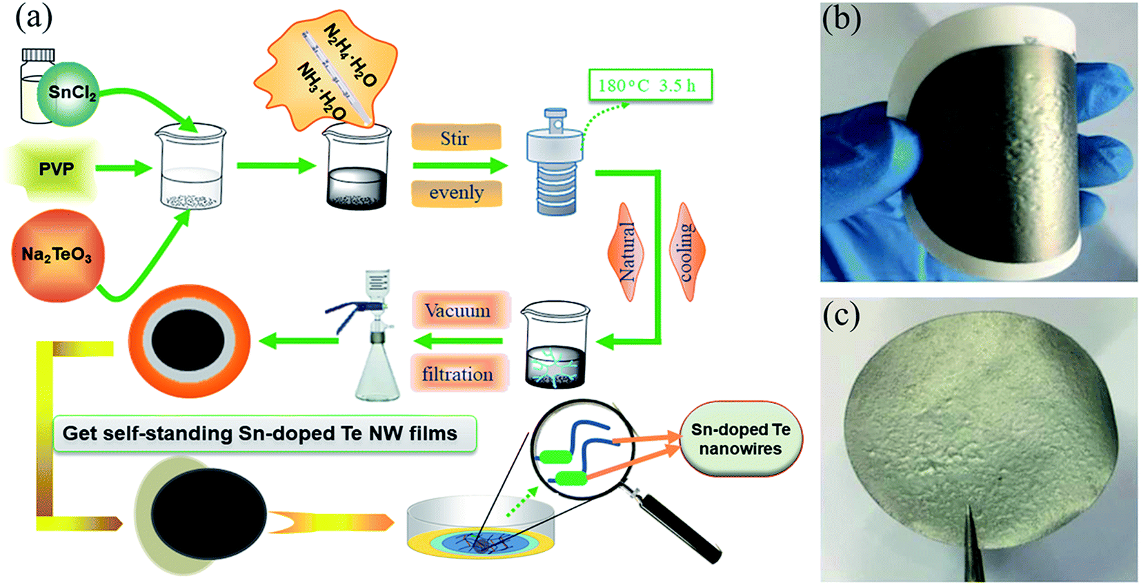 | ||
| Fig. 1 Schematic diagram of (a) the preparation of Sn-doped Te NWs thin films, (b) the prepared flexible Sn-doped Te NWs films, and (c) self-standing Sn-doped Te NWs films. | ||
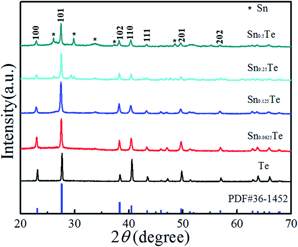 | ||
| Fig. 2 XRD patterns of pure Te NWs and SnTe NWs with different Sn contents. | ||
Fig. 3 presents the surface morphology of the un-doped and Sn-doped Te NW films. The SEM image in Fig. 3a demonstrated that the pure Te NWs showed a relative uniform 1D structure as previously reported in literature.41 The surface structure showed no change except for a slight diameter increase after the small addition of Sn in Te for Sn0.125Te NWs, as shown in Fig. 3b. In Fig. 3c, nanoparticles were observed on the surface of Te/Sn NWs when the molar radio of Sn/Te increased to 0.25. The mechanism for forming a Te-based nanostructure was generally attributed to its anisotropic structure.42,43 The intrinsic Te crystal consists of layers stacked along the c-axis with week van der Waals bonds that dominate the shape of primary Te nanoparticles. The homogeneous surface is due to the stabilizing agent, temperature, reductive power of reducing agents, etc. The observed nanoparticles were attributed to the excess Sn or Te/Sn nanoparticles.44 In Fig. 3d, an increase in the Sn/Te molar radio to 0.50 resulted in the presence of larger nanoparticles, indicating the significant influence of Sn content on the morphology of Te/Sn NWs.
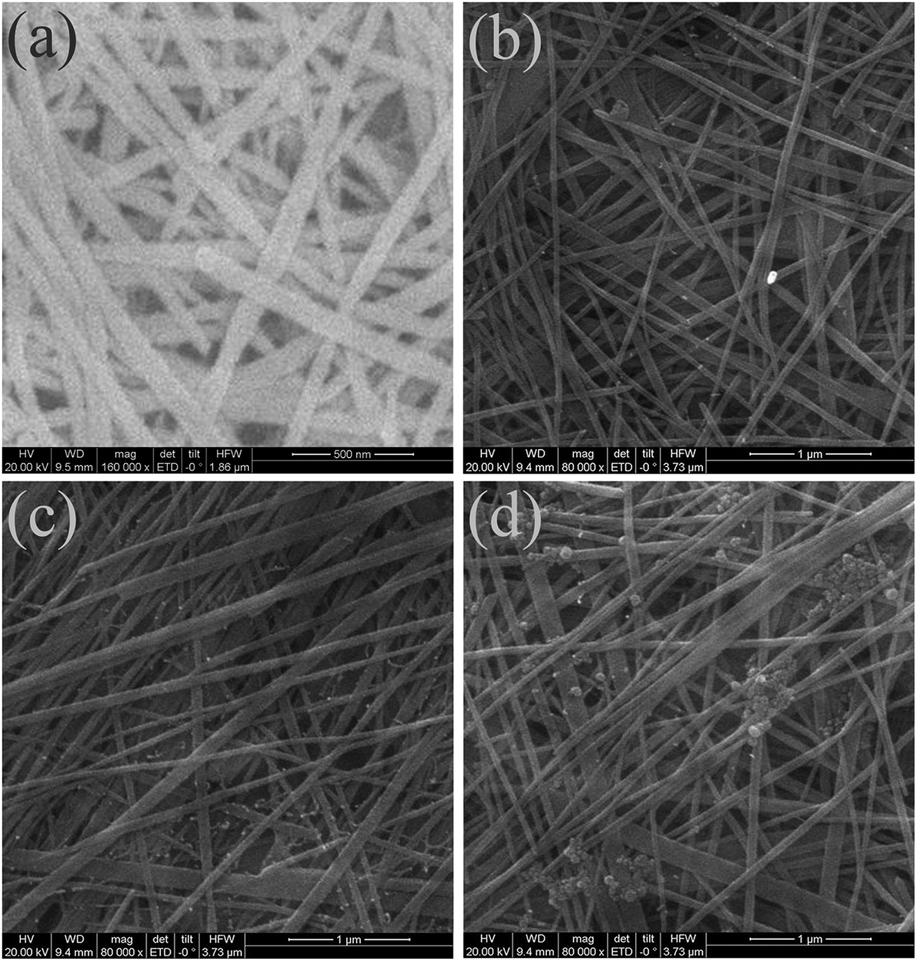 | ||
| Fig. 3 SEM images of (a) Te NWs, (b) Sn0.125Te, (c) Sn0.25Te, and (d) Sn0.50Te NWs. | ||
TEM images were obtained to further reveal the morphological structure of SnTe NWs, as shown in Fig. 4. The TEM image of pure Te displayed a 1D homogeneous NW structure with small diameter of 15–20 nm in Fig. 4a. The lattice spacing in the HR-TEM image was measured at 0.59 nm in the inset of Fig. 4a, corresponding to the c-axis diffraction pattern of the trigonal Te phase structure. The TEM image of the Sn0.125Te NWs in Fig. 4b presented a similar morphology to Te NWs with an increased average diameter of 58 ± 7.5 nm. The lattice spacing for SnTe was not visually apparent in the corresponding HR-TEM image owing to the low molar amount of Sn in the as-synthesized samples, further indicating the dominated Te phase in SnTe with low Sn content.
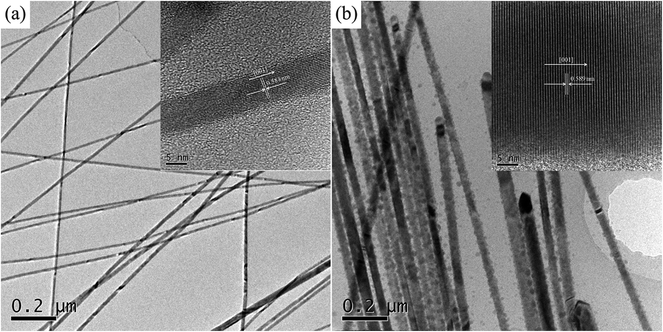 | ||
| Fig. 4 TEM images of the as-prepared (a) Te NWs and (b) Sn0.125Te NWs. | ||
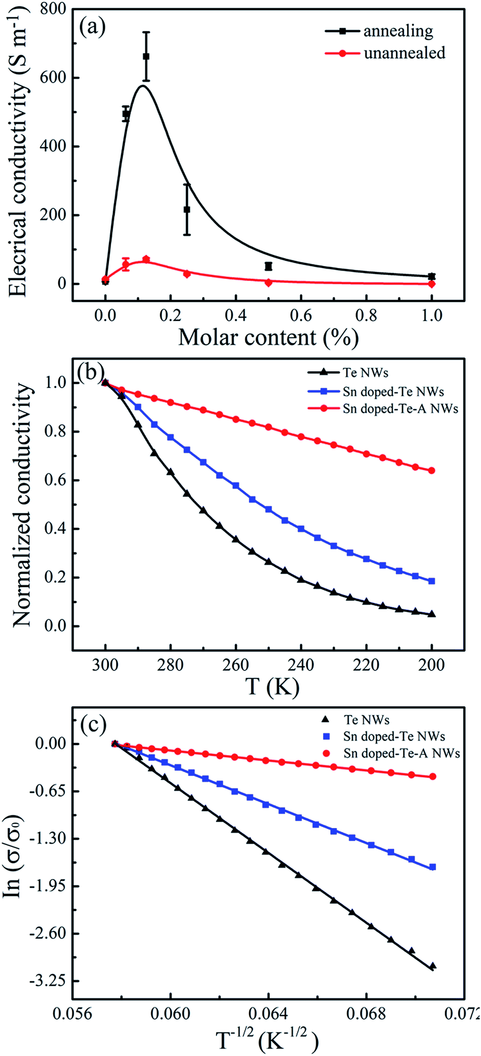
Fig. 5 shows the electrical conductivity of the Sn-doped Te NWs films as a function of Sn content before and after annealing. The pure Te NWs films had a low electrical conductivity of 8 ± 3 S m−1 in Fig. 5a, which was detrimental for high-performance TE materials. An optimized electrical conductivity of 71.5 S m−1 was obtained for Sn0.125Te NWs films. As expected, doping with Sn element enhanced the electrical conductivity of Te NWs films at room temperature due to the change in inherent valance band structure. When the Sn content was more than 20%, the electrical conductivity of Te/Sn NW films decreased, which may be due to the excess Sn element leading to the change in structure as observed in the XRD spectra from Fig. 2. Theoretical calculations suggest that the electrical conductivity of Te NWs films would be significantly increased by doping with metal elements due to the synergies and valence band convergence.14 The intrinsic Sn deficiency enabled a highly degenerate p-type SnTe with a large hole concentration ca. 1021 cm−3.28 This similar phenomenon was also observed in Bi-doped Te ingots.21 As shown in Fig. 5a, the electrical conductivity of the SnTe NWs films increased after annealing at 300 °C for 3.5 h. The highest electrical conductivity as 663 S m−1 was achieved for Sn0.125Te. Annealing resulted in an electrical conductivity that was one order of magnitude larger than that without annealing. For further explanation of the changes in electrical conductivity, carrier concentration (n) and mobility (μ) were measured as listed in Table 1. Sn0.125Te showed a large improvement in the carrier concentration compared to that of pure Te NWs with a decreased mobility. This finding suggested that Sn-doping can effectively adjust the inherent valence band structure, which was consistent with metal-doped samples reported in literatures.26,45
 | ||
| Fig. 5 (a) Curves of the electrical conductivity for Sn-doped Te NWs films with different Sn content before and after annealing. (b) Temperature dependence of the normalized electrical conductivity of Te and Sn-doped Te NWs films. (c) Analyses of the temperature dependence of the electrical conductivity with the 1D VRH model. | ||
| Samples | n (1018 cm−3) | μ (cm2 V−1 S−1) | σ c (S m−1) | σ m (S m−1) |
|---|---|---|---|---|
| a The calculated electrical conductivity (σc) based on σ = neμ. b The measured electrical conductivity (σm) with a standard four-point-probe technique. | ||||
| Te NWs | 0.0166 | 33.7 | 8.9 | 8 |
| Sn0.125Te NWs | 30.6 | 0.17 | 83.2 | 80 |
| Sn0.125 Te-A NWs | 3.6 | 13.7 | 789 | 663 |
In addition, due to the strong interaction between Te and PVP, the complete removal of residual PVP on the surface of Te NWs is quite difficult, leading to a high energy barrier and low electrical conductivity.46,47 The annealing process at 300 °C for 3.5 hours resulted in degradation and carbonization, leading to a decreased energy barrier and increased contact among NWs.37 Therefore, the enhanced electrical conductivity of Sn-doping Te NW films was attributed to three reasons: (i) the state density at the Fermi level and crystal structure of Te NWs films were changed after Sn element doping,48 (ii) Sn-doping with proper content enhanced the carrier concentration of Te NWs; and (iii) the degradation of partially residual insulated PVP after annealing resulted in better contact between adjacent NWs.37
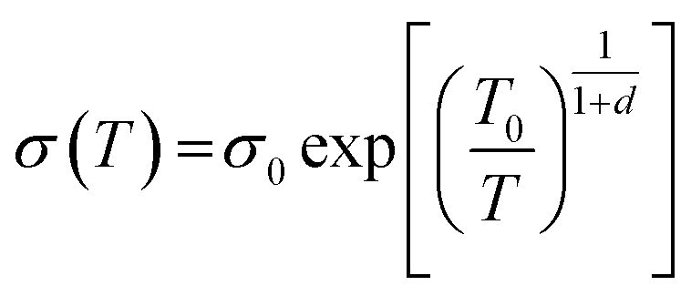
Fig. 5b shows the temperature dependence on the normalized electrical conductivity of as-prepared films to further reveal conductive properties. The electrical conductivity decreased as the temperature decreased, indicating typical semiconductor behavior. The analyses of temperature dependence on electrical conductivity using the variable range hoping (VRH) model was performed as displayed in Fig. 5c. The VRH mechanism can be described by
 | (1) |
121, 17689 and 1156 K, respectively. The T0 is related to the electronic density of states of N (EF) near the Fermi energy level (EF).49,50 The Sn-doping reduced the T0 value. This finding resulted in a decrease in the carrier hopping barrier and an enhancement in the electronic transmission capability. These results were consistent with the changes in electrical conductivity, carrier concentration, and carrier mobility for the as-prepared films.
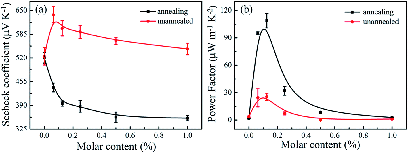
Fig. 6 presents the S and calculated S2σ for Sn-doped Te NWs films with different Sn element content. The pure Te NWs film had a high Seebeck coefficient at ∼524.6 μV K−1 before annealing, which was higher than previously reported values.21,51 The positive Seebeck coefficient values suggest that the Te and SnTe NWs are typical p-type semiconductors. Generally, SnTe has a large hole concentration ca. 1021 cm−3. Owing to the intrinsic deficiency of Sn, SnTe is considered to be a highly degenerate p-type semiconductor.28 In general, the Seebeck coefficient of the sample is inversely proportional to the carrier concentration, which is predicted by nondegenerate semiconductors according to the Boltzmann formula,52,53
 | (2) |
 | ||
| Fig. 6 Seebeck coefficient (a) and power factor (b) of the Sn-doped Te NWs films as a function of Sn content. | ||
Fig. 6b demonstrates that the power factor (S2σ) underwent a major enhancement after doping with the Sn element before and after annealing. The pure Te NWs film produced a low power factor of 3.61 μW m−1 K−2. The power factor of the prepared Sn-doped Te NWs films slightly increased before annealing and a maximum power factor of 25.35 μW m−1 K−2 was obtained for Sn0.125Te NWs films. An optimal power factor of 114.6 μW m−1 K−2 for Sn0.125Te NWs thin film was achieved after annealing, which was an order of magnitude higher than that of the pure Te NWs film. The increase in the power factor after annealing was due to the significant increase in electrical conductivity with a small decrease in the Seebeck coefficient (395.2 μV K−1). The electrical conductivity of pristine SnTe by Spark Plasma Sintering (SPS) was ∼7000 S cm−1.56 The Sn0.125Te NWs film in this work had a high power factor due to the large Seebeck coefficient. The prepared Sn-doped Te NWs films after annealing presented better TE performance compared to Sn-doped Te ingots. However, the SnTe exhibited a lower power factor than other metal elements (such as Sb, Bi, and doped Te) due to the unsatisfactory electrical conductivity without SPS technology.21,26 In addition, the 1D Te NWs film presented intrinsically low thermal conductivity at 0.146 W m−1 K−1 (ref. 16) compared to Te-based ingots. This finding was due to the low density of the formed NWs network in film and high phonon scattering of 1D NWs.57,58 Therefore, the Sn-doped Te NWs with low Sn content provided a novel means to optimize the TE performance of inorganic nanomaterials.
Conclusions
In summary, the lead-free metal, Sn, was successfully employed to enhance the TE performance of Te NWs films using a simple hydrothermal method. The use of as-synthesized Sn-doped Te NWs with low Sn content resulted in a significant enhancement in the electrical conductivity and high power factor after annealing. The optimal power factor of 114.6 μW m−1 K−2 for Sn0.125Te NWs thin film after annealing was achieved at room temperature, which was about two orders of magnitude higher than the pure Te NWs and reported pristine SnTe. An Sn/Te atom ratio higher than 0.20 resulted in the 1D Te/Sn NWs demonstrating a compound phase of Sn and a decrease in TE performance. These results provide a promising way to regulate the carrier concentration and power factor of low-dimensional nanomaterials by effective electron and phonon structure control.Conflicts of interest
There are no conflicts to declare.Acknowledgements
This work was financially supported by the National Natural Science Foundation of China (51762018, 51463008, 51572117, and 21563013), and the Innovation Driven “5511” Project of Jiangxi Province (20165BCB8016).References
- G. Tan, S. Hao, R. C. Hanus, X. Zhang, S. Anand, T. P. Bailey, A. J. E. Rettie, X. Su, C. Uher, V. P. Dravid, G. J. Snyder, C. Wolverton and M. G. Kanatzidis, ACS Energy Lett, 2018, 3, 705–712 CrossRef.
- L. E. Bell, Science, 2008, 321, 1457–1461 CrossRef PubMed.
- L. Yang, Z. Chen, M. S. Dargusch and J. Zou, Adv. Energy Mater., 2018, 8, 1701797 CrossRef.
- J. P. Rojas, D. Singh, S. B. Inayat, G. A. T. Sevilla, H. M. Fahad and M. M. Hussain, ECS J. Solid State Sci. Technol., 2017, 6, 3036–3044 CrossRef.
- C. Romo-De-La-Cruz, L. Liang, S. A. P. Navia, Y. Chen, J. Prucz and X. Song, Sustainable Energy Fuels, 2018, 2, 876–881 RSC.
- H. An, D. Karas, B. W. Kim, S. Trabia and J. Moon, Nanotechnology, 2018, 29, 275403 CrossRef PubMed.
- L. D. Hicks and M. S. Dresselhaus, Phys. Rev. B, 1993, 47, 16631–16634 CrossRef.
- A. Ali, Y. Chen, V. Vasiraju and S. Vaddiraju, Nanotechnology, 2017, 28, 282001 CrossRef PubMed.
- R. A. Kishore, P. Kumar and S. Priya, Sustainable Energy Fuels, 2018, 2, 175–190 RSC.
- J. Kim, J. Bahk, J. Hwang, H. Kim, H. Park and W. Kim, Phys. Status Solidi RRL, 2013, 7, 767–780 CrossRef.
- S. Hashimoto, S. Asada, T. Xu, S. Oba, Y. Himeda, R. Yamato, T. Matsukawa, T. Matsuki and T. Watanabe, Appl. Phys. Lett., 2017, 111, 023105 CrossRef.
- H. Fang, H. Yang and Y. Wu, Chem. Mater., 2014, 26, 3322–3327 CrossRef.
- Z. He, Y. Yang, J. W. Liu and S. H. Yu, Chem. Soc. Rev., 2017, 46, 2732–2753 RSC.
- H. Peng, N. Kioussis and G. J. Snyder, Phys. Rev. B, 2014, 89, 1–7 Search PubMed.
- S. Lin, W. Li, Z. Chen, J. Shen, B. Ge and Y. Pei, Nat. Commun., 2016, 7, 10287 CrossRef PubMed.
- W. Wang, C. Li, X. Li, Y. Jia, F. Jiang, C. Liu, R. Tan and J. Xu, Thin Solid Films, 2018, 654, 12–29 Search PubMed.
- Z. Wang, T. Araki, T. Onda and Z. Chen, J. Mater. Sci., 2018, 53, 9117–9130 CrossRef.
- L. D. Hicks, T. C. Harman, X. Sun and M. S. Dresselhaus, Phys. Rev. B, 1996, 56, 493–496 Search PubMed.
- C. Li, P. Sun, C. Liu, J. Xu, T. Wang, W. Wang, J. Hou and F. Jiang, J. Alloys Compd., 2017, 723, 642–648 CrossRef.
- A. Banik, U. S. Shenoy, S. Saha, U. V. Waghmare and K. Biswas, J. Am. Chem. Soc., 2016, 138, 13068–13075 CrossRef PubMed.
- X. Qian, Y. Xiao, L. Zheng, B. Qin, Y. Zhou, Y. Pei, B. Yuan, S. Gong and L. Zhao, RSC Adv., 2017, 7, 17682–17688 RSC.
- C. Fu, H. Wu, Y. Liu, J. He, X. Zhao and T. Zhu, Adv. Sci., 2016, 3, 1600035 CrossRef PubMed.
- M. Yang, T. Su, H. Zhu, S. Li, M. Hu, Q. Hu, H. Ma and X. Jia, J. Mater. Sci., 2018, 53, 11524–11533 CrossRef.
- J. Q. Li, N. Yang, S. M. Li, Y. Li, F. S. Liu and W. Q. Ao, J. Electron. Mater., 2017, 47, 205–211 CrossRef.
- M. Yang, T. Su, D. Zhou, H. Zhu, S. Li, M. Hu, Q. Hu, H. Ma and X. Jia, J. Mater. Sci., 2017, 52, 10526–10532 CrossRef.
- S. Lin, W. Li, X. Zhang, J. Li, Z. Chen and Y. Pei, Inorg. Chem. Front., 2017, 4, 1066–1072 RSC.
- Q. Zhang, B. Liao, Y. Lan, K. Lukas, W. Liu, K. Esfarjani, C. Opeil, D. Broido, G. Chen and Z. Ren, Proc. Natl. Acad. Sci., 2013, 110, 13261–13266 CrossRef PubMed.
- G. Tan, L. D. Zhao, F. Shi, J. W. Doak, S. H. Lo, H. Sun, C. Wolverton, V. P. Dravid, C. Uher and M. G. Kanatzidis, J. Am. Chem. Soc., 2014, 136, 7006–7017 CrossRef PubMed.
- A. Banik, U. S. Shenoy, S. Anand, U. V. Waghmare and K. Biswas, Chem. Mater., 2015, 27, 581–587 CrossRef.
- G. Tan, F. Shi, J. W. Doak, H. Sun, L. Zhao, P. Wang, C. Uher, C. Wolverton, V. P. Dravid and M. G. Kanatzidis, Energy Environ. Sci., 2015, 8, 267–277 RSC.
- H. Wu, C. Chang, D. Feng, Y. Xiao, X. Zhang, Y. Pei, L. Zheng, D. Wu, S. Gong, Y. Chen, J. He, M. G. Kanatzidis and L. Zhao, Energy Environ. Sci., 2015, 8, 3298–3312 RSC.
- L. Zhang, J. Wang, Z. Cheng, Q. Sun, Z. Li and S. Dou, J. Mater. Chem. A, 2016, 4, 7936–7942 RSC.
- D. Feng, Z. Ge, Y. Chen, J. Li and J. He, Nanotechnology, 2017, 28, 455707 CrossRef PubMed.
- P. V. More, C. Hiragond, A. Dey and P. K. Khanna, Sustainable Energy Fuels, 2017, 1, 1766–1773 RSC.
- G. Tan, W. G. Zeier, F. Shi, P. Wang, G. J. Snyder, V. P. Dravid and M. G. Kanatzidis, Chem. Mater., 2015, 27, 7801–7811 CrossRef.
- E. Xu, Z. Li, J. Martinez, N. Sinitsyn, H. Htoon, N. Li, B. Swartzentruber, J. Hollingsworth, J. Wang and S. Zhang, Nanoscale, 2015, 7, 2869–2876 RSC.
- C. Li, F. Jiang, C. Liu, W. Wang, X. Li, T. Wang and J. Xu, Chem. Eng. J., 2017, 320, 201–210 CrossRef.
- R. Cecchini, S. Selmo, C. Wiemer, E. Rotunno, L. Lazzarini, M. De Luca, I. Zardo and M. Longo, Mater. Res. Lett., 2017, 6, 29–35 CrossRef.
- C. Li, F. Kong, C. Liu, H. Liu, Y. Hu, T. Wang, J. Xu and F. Jiang, Nanotechnology, 2017, 28, 235604 CrossRef PubMed.
- M. Sist, E. M. J. Hedegaard, S. Christensen, N. Bindzus, K. F. F. Fischer, H. Kasai, K. Sugimoto and B. B. Iversen, IUCrJ, 2016, 3, 377–388 CrossRef PubMed.
- B. Luo, B. Wang, M. Liang, J. Ning, X. Li and L. Zhi, Adv. Mater., 2012, 24, 1405–1409 CrossRef PubMed.
- W. Lu, Y. Ding, Y. Chen, Z. Wang and J. Fang, J. Am. Chem. Soc., 2005, 127, 10112–10116 CrossRef PubMed.
- J. Mi, N. Lock, T. Sun, M. Christensen, M. Sondergaard, P. Hald, H. Hng, J. Ma and B. Iversen, ACS Nano, 2010, 4, 2523–2530 CrossRef PubMed.
- Z. Zheng, F. Li, J. Luo, G. Liang, H. Ma, X. Zhang and P. Fan, Mater. Lett., 2017, 209, 455–458 CrossRef.
- D. Ibrahim, V. Ohorodniichuk, C. Candolfi, C. Semprimoschnig, A. Dauscher and B. Lenoir, ACS Omega, 2017, 2, 7106–7111 CrossRef.
- M. Luo, Y. Hong, W. Yao, C. Huang, Q. Xu and Q. Wu, J. Mater. Chem. A, 2015, 3, 2770–2775 RSC.
- K. Wang, H. Liang, W. Yao and S. Yu, J. Mater. Chem., 2011, 21, 15057–15062 RSC.
- L. D. Hicks and M. S. Dresselhaus, Phys. Rev. B, 1993, 47, 12727–12731 CrossRef.
- G. Zheng, Y. Sun and X. Zhu, Phys. Lett. A, 2006, 355, 66–72 CrossRef.
- G. Zheng, Z. Dai, Y. Dong, Y. Zhang, Y. Ma, H. Zhang and G. Li, J. Low Temp. Phys., 2011, 165, 43–54 CrossRef.
- K. C. See, J. P. Feser, C. E. Chen, A. Majumdar, J. J. Urban and R. A. Segalman, Nano Lett., 2010, 10, 4664–4667 CrossRef PubMed.
- X. Zhang, Y. Zhou, Y. Pei, Y. Chen, B. Yuan, S. Zhang, Y. Deng, S. Gong, J. He and L. Zhao, J. Alloys Compd., 2017, 709, 575–580 CrossRef.
- S. H. Zaferani, Renewable Sustainable Energy Rev., 2017, 71, 359–364 CrossRef.
- Z. Lin, C. Hollar, J. S. Kang, A. Yin, Y. Wang, H. Y. Shiu, Y. Huang, Y. Hu, Y. Zhang and X. Duan, Adv. Mater., 2017, 29, 1606662 CrossRef PubMed.
- R. F. Brebrick and A. J. Strauss, Phys. Rev., 1963, 131, 104–110 CrossRef.
- L. Zhao, X. Zhang, H. Wu, G. Tan, Y. Pei, Y. Xiao, C. Chang, D. Wu, H. Chi, L. Zheng, S. Gong, C. Uher, J. He and M. Kanatzidis, J. Am. Chem. Soc., 2015, 138, 2366–2373 CrossRef PubMed.
- C. Shang, M. Yang, Z. Wang, M. Li, M. Liu, J. Zhu, Y. Zhu, L. Zhou, H. Cheng, Y. Gu, Y. Tang, X. Zhao and Z. Lu, Sci. China Mater., 2017, 60, 937–946 CrossRef.
- J. Li, Sci. China Mater., 2017, 60, 1023–1024 CrossRef.
Footnote |
| † These authors contributed equally. |
| This journal is © The Royal Society of Chemistry 2018 |