
Layered hybrid perovskite solar cells based on single-crystalline precursor solutions with superior reproducibility†
Yangyang
Dang‡
ac,
Jing
Wei‡
 b,
Xiaolong
Liu
a,
Xi
Wang
b,
Kun
Xu
b,
Ming
Lei
*b,
Wenping
Hu
*c and
Xutang
Tao
*a
b,
Xiaolong
Liu
a,
Xi
Wang
b,
Kun
Xu
b,
Ming
Lei
*b,
Wenping
Hu
*c and
Xutang
Tao
*a
aInstitute of Crystal Materials, State Key Laboratory of Crystal Materials, Shandong University, No. 27 Shanda South Road, Jinan, 250100, P. R. China. E-mail: txt@sdu.edu.cn
bState Key Laboratory of Information Photonics and Optical Communications, School of Science, Beijing University of Posts and Telecommunications, Beijing, 100876, P. R. China. E-mail: mlei@bupt.edu.cn
cTianjin Key Laboratory of Molecular Optoelectronic Sciences, Department of Chemistry, School of Sciences, Collaborative Innovation Center of Chemical Science and Engineering, Tianjin University, Tianjin, 300072, P. R. China. E-mail: huwp@tju.edu.cn
First published on 19th July 2018
Abstract
Restrained by the difficulties in the stability, crystal processing, and single-crystalline device fabrication based on the prototype perovskite of CH3NH3PbI3, there is a growing interest in finding a way to introduce long-chain organic ammonium into CH3NH3PbI3 to tackle these challenges, leading to emerging layered perovskite materials. Here, we first report the bulk crystal growth in an ambient atmosphere on single crystals of layered perovskite (n-C4H9NH3)2(CH3NH3)n−1PbnI3n+1 (n = 1, 3, and 4) obtained using fine control of the molar ratio of perovskite precursors by the top seeded solution growth (TSSG) method. The fundamental properties (band gap, PL spectra and thermal stability) of (n-C4H9NH3)2(CH3NH3)n−1PbnI3n+1 (n = 1, 3, and 4) single crystals are investigated. More importantly, we investigated the formation of (n-C4H9NH3)2(CH3NH3)n−1PbnI3n+1 (n = 3 and 4) thin films based on their single-crystalline precursors by a modified hot-casting method, which makes it easier to obtain uniformly oriented thin films to help improve the photovoltaic performance and reproducibility. And solar cells fabricated based on these thin films exhibited a power conversion efficiency (PCE) of 5.05% (n = 3) and 9.03% (n = 4), and demonstrated good feasibility and stability. These attractive results may provide an understanding for further studies of the optoelectronic device applications of these layered perovskite materials.
Introduction
Organic–inorganic hybrid lead halides with perovskite crystal structures have attracted significant interest due to their peculiar properties, such as carrier mobility,1–3 phase transitions,4 photoluminescence,5 ferroelectricity,6–10 thermoelectric properties11,12 and photoconductivity.13 These materials have been used as emerging solar absorbers with impressive photovoltaic characteristics.14 For example, a prompt rise in the power conversion efficiency from 3.8% (ref. 15) to 22.7% (ref. 16) has been witnessed in the past seven years. However, the poor stability of devices based on these perovskites is the main concern at present. Compared with 3-dimensional (3D) hybrid perovskites with the ABX3 structure, 2D layered A2MX4 analogue-based perovskite materials with layered crystal structures (where A is aliphatic or aromatic amine, M is ordinarily Sn or Pb, and X is usually Cl, Br or I) exhibit excellent stability and have received increasing attention.17 The syntheses and properties of (n-C4H9NH3)2(CH3NH3)n−1SnnI3n+1 (n-C4H9NH3 = BA; CH3NH3 = MA; n= an integer) layered perovskite materials were first investigated by the Mitzi group.18 Later, the Kanatzidis group reported the syntheses, crystal structure and relevant properties of layered perovskites based on BA2MAn−1PbnI3n+1.17,19 And planar (BA)2(MA)2Pb3I10 solar cells with the maximum PCE of 4.02% were also investigated.17 Recently, 12.52% power conversion efficiency solar cells with enhanced moisture stability using BA2MAn−1PbnI3n+1 as the photo-absorber have been reported by the Kanatzidis group and the Mohite group.20 Generally, the applications of layered perovskites in opto-electronic devices including solar cells,21 field-effect transistors (FETs),22 or light-emitting diodes (LEDs)23 are based on polycrystalline thin films. To date, there have been few reports on bulk crystal growth and the fundamental properties of these layered perovskite single crystals together with their solar cell fabrication, which to some degree may be ascribed to the lack of fine control over the crystal growth on these materials.In this work, we reported the bulk growth and intrinsic properties of BA2MAn−1PbnI3n+1 (n = 1, 3, and 4) single crystals. By control of the number of perovskite layers (n), the band gap was systematically tuned. More importantly, the formation processes of BA2MAn−1PbnI3n+1 thin films based on their single-crystalline precursors by a modified hot-casting method were demonstrated for the first time. Solar cells based on BA2MAn−1PbnI3n+1 (n = 3 and 4) single-crystalline precursor solutions exhibited good stability with PCEs of 5.05% and 9.03%, with the increase of the number of perovskite layers (n), which showed superior reproducibility. These attractive features may enable interesting opportunities to apply emerging layered single crystalline materials for environmentally stable optoelectronic devices.
Results and discussion
As a base for this study, we grew high quality bulk BA2MAn−1PbnI3n+1 (n = 1, 3, and 4) single crystals in an ambient atmosphere with the top-seeded solution growth (TSSG) method (see Fig. 1 and S1, in the ESI†). Given the difficulty in obtaining bulk BA2MAn−1PbnI3n+1 (n = 3 and 4) single crystals, it is necessary to finely control the molar ratio of BAI, MAI and PbO to yield desired formation of bulk BA2MAn−1PbnI3n+1 (n = 3 and 4) single crystals with the desired stoichiometric ratio. Here, freshly synthesized BAI and MAI were reacted with PbO in HI solutions at 65 °C under an ambient atmosphere. The molar ratio of BAI, MAI and PbO in BA2MAn−1PbnI3n+1 (n = 3 and 4) was 2![[thin space (1/6-em)]](https://www.rsc.org/images/entities/char_2009.gif) :2.5:3 and 2:4:4, respectively. To obtain high quality bulk perovskite single crystals, the conditions for crystallization were carefully optimized including the appropriate growth temperature and selection of high-quality seed crystals. The morphologies of plate- and block-shaped BA2MAn−1PbnI3n+1 (n = 3 and 4) single crystals were obtained based on seed crystals along different crystallographic directions (see Fig. 1). The powder X-ray diffraction patterns of BA2MAn−1PbnI3n+1 (n = 1, 3, and 4) single crystals well agree with the calculated single-crystal XRD patterns shown in Fig. S2 (ESI).†
:2.5:3 and 2:4:4, respectively. To obtain high quality bulk perovskite single crystals, the conditions for crystallization were carefully optimized including the appropriate growth temperature and selection of high-quality seed crystals. The morphologies of plate- and block-shaped BA2MAn−1PbnI3n+1 (n = 3 and 4) single crystals were obtained based on seed crystals along different crystallographic directions (see Fig. 1). The powder X-ray diffraction patterns of BA2MAn−1PbnI3n+1 (n = 1, 3, and 4) single crystals well agree with the calculated single-crystal XRD patterns shown in Fig. S2 (ESI).†
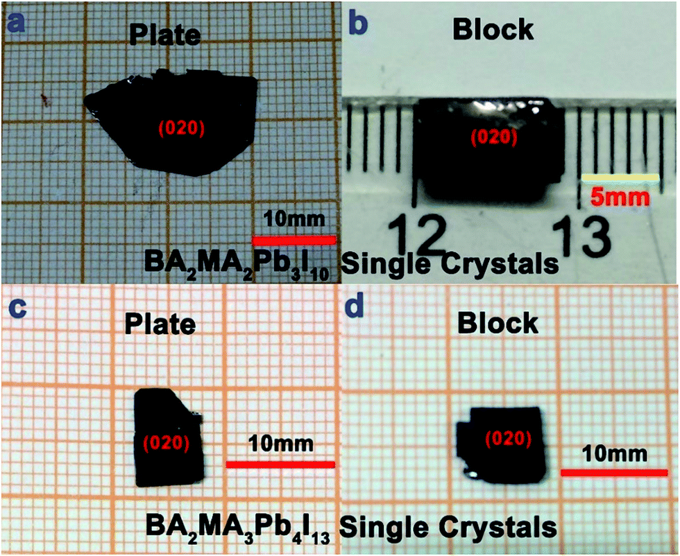 | ||
| Fig. 1 Pictures of plate- and block-shaped single crystals of BA2MA2Pb3I10 (a and b) and BA2MA3Pb4I13 (c and d) obtained by using the TSSG method. | ||
As shown in Fig. 1 and S1,† BA2MAn−1PbnI3n+1 (n = 1, 3, and 4) single crystals exhibit an obvious layered growth habit, when compared with bulk MAPbI3 single crystals. The mainly displayed facet of BA2MA2Pb3I10 and BA2MA3Pb4I13 single crystals was determined to be (020) by X-ray diffraction, which differs from that ((002) facet) of BA2PbI4 crystals . Fig. S3 (ESI†) shows the calculated theoretical morphologies of BA2MAn−1PbnI3n+1 (n = 1, 3, and 4) single crystals at room temperature based on the Bravais–Friedel–Donnay–Harker (BFDH) method24,25 (Mercury 3.3 version25). Clearly, BA2MAn−1PbnI3n+1 (n = 1, 3, and 4) single crystals were all found to represent an orthorhombic lattice structure with a nonpolar point group mmm at room temperature by single-crystal X-ray diffraction.26 BA2PbI4 was determined to belong to the space group Pbca in Table S1,† which agreed with the former results reported by Billing et al.27 and Mitzi et al.28 Differently, BA2MA2Pb3I10 and BA2MA3Pb4I13 were found to crystallize in the polar space groups C2cb and Cc2m, respectively, as reported by Kanatzidis et al.19 In our case, the attained BA2MA2Pb3I10 and BA2MA3Pb4I13 both exhibit the space groups Cmca and Ccmm, which are also similar to the nonpolar space groups Acam and Ccmm reported by Kanatzidis et al.19 Moreover, the crystal structure of BA2MA2Pb3I10 is similar to that of BA2MA2Sn3I10 reported by Mitzi et al.18 As shown in Fig. S4(a–c),† BA2MAn−1PbnI3n+1 (n = 1, 3, and 4) exhibited evident layered crystal structures along the [001] or [010] direction, respectively.
The band gap (Eg) of these crystals was calculated based on UV-vis absorption spectra with the Kubelka–Munk function (see Fig. S5†).29–34 The determined Eg is 2.21 eV, 1.76 eV and 1.63 eV for BA2MAn−1PbnI3n+1 with n = 1, 3, and 4, respectively. Similarly, the tunable PL spectra of BA2MAn−1PbnI3n+1 (n = 1, 3, and 4) single crystals are located at 519 nm, 650 nm and 687 nm, respectively in Fig. S6.† The thick BA2MAn−1PbnI3n+1 (n = 3 and 4) single crystals exhibited shoulder or broad peaks and red-shifted PL phenomena. However, the thin BA2MAn−1PbnI3n+1 (n = 3 and 4) single crystals exhibited narrow PL peaks in Fig. S7,† which were consistent with those previously reported by Blancon et al.35 These results demonstrated that the thickness resulted in shoulder or broad PL peaks, and red-shifted PL phenomena. The increased band gaps and blue-shifted PL spectra with respect to that of MAPbI3, tunable by the number of the organic spacer layer (or n) in BA2MAn−1PbnI3n+1 (n = 1, 3, and 4) may be attributed to the reduced disorder in the dipole of MA+ cations within the crystal lattice. BA2MAn−1PbnI3n+1 (n = 1, 3, and 4) single crystals have been identified to be direct band gap semiconductors, as reported by Kanatzidis et al.19 This feature benefits the optoelectronic applications of these materials. Next, we examine the stability of 2D layered perovskites. Fig. S8† shows the results of TGA and DSC measured on BA2MAn−1PbnI3n+1 (n = 1, 3, and 4). Clearly, the decomposition temperature of BA2MA2Pb3I10 and BA2MA3Pb4I13 is higher than that of BA2PbI4 in Fig. S8.† This advantage promotes realistic applications of this class of materials for opto-electronic devices.
Fig. 2 demonstrates the schematic of the BA2MAn−1PbnI3n+1 perovskite thin film formation process based on single-crystalline precursors by a modified hot-casting method, which makes it easier to obtain uniformly oriented thin films to help improve the photovoltaic performance and reproducibility. This process mainly includes three steps: (a) BA2MAn−1PbnI3n+1 (n = 3 and 4) single crystals are dissolved in N,N-dimethylformamide (DMF) solvent; (b) an intermediate phase MAPbI3–DMF complex solution is formed, while BA+ cations separate and exist in the solution. And then the solution was spun-cast at 3500 rpm on preheated FTO/compact TiO2/mesoporous TiO2 based substrates, as shown in Fig. 3(a), and chlorobenzene is added as an anti-solvent; (c) the precursor thin films soon change into a final layered perovskite phase in the spin coating process. The key step in the above process based on single-crystalline precursors is the formation of the intermediate phase MAPbI3–DMF complex solution, which agrees with that previously reported by the Kanatzidis group.36 However, in previous reports about perovskite solar cell fabrication, PbI2 was dissolved in DMF or dimethyl sulfoxide (DMSO) solvent and then formed into a PbI2–DMF or PbI2–DMSO complex intermediate, which may bring in extra PbI2 impurities or defects in the final perovskite film.37–43 However, the BA2MAn−1PbnI3n+1 (n = 3 and 4) thin films exhibited impure peaks of XRD in Fig. S9,† causing lower PCEs of solar cells based on them than those based on single-crystalline precursors. This speculation can also be confirmed by a similar CH(NH2)2SnI3 (FASnI3) film formation process. Brown FASnI3 thin films in Fig. S10a† were formed by SnI2 combined with FAI in DMSO solvent, which exhibited no PCEs. Contrastively, black FASnI3 thin films were formed by FASnI3 single-crystalline precursors in DMSO solvent, which exhibited good stability and a PCE of 1.08% with the structure architectures of ITO/PEDOT:PSS/FASnI3/PC61BM and [6,6]-phenyl-C61-butyric acid methyl ester/ZnO nanoparticles/aluminum under standard air-mass 1.5 global (AM 1.5G) illumination, as shown in Fig. S10(b and c) and Table S2.† This result also verified the feasibility of photovoltaic fabrication based on single-crystalline precursors. These features should provide guidance for the preparation and fabrication of optoelectronic devices.
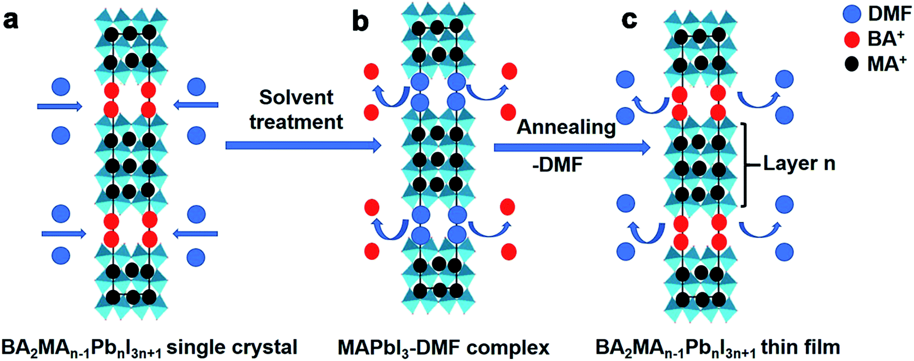 | ||
| Fig. 2 (a–c) The formation processes of BA2MAn−1PbnI3n+1 (n = 3 and 4) thin films based on their single-crystalline precursors by a modified hot-casting method. | ||
 | ||
| Fig. 3 The device architectures of BA2MAn−1PbnI3n+1 (n = 3 and 4) solar cells based on their single-crystalline precursors by a modified hot-casting method. | ||
Furthermore, the SEM images of the photovoltaic device structures based on BA2MAn−1PbnI3n+1 (n = 3 and 4) thin film solar cell device structures are shown in Fig. 4(a and d). And the SEM images of BA2MAn−1PbnI3n+1 (n = 3 and 4) thin films are illustrated in Fig. 4(b and e). In 2016, Tsai et al. reported 12.52% PCE planer solar cells based on BA2MAn−1PbnI3n+1 exhibiting two planes (−11−1) and (202).20 In our results, we observed the XRD peaks of the BA2MA2Pb3I10 thin film from Fig. 4(b) located at 2θ = 14.16°, 28.54°, 43.40° and 59.08°, while the XRD peaks of the BA2MA3Pb4I13 thin film from Fig. 4(e) were located at 2θ = 14.12°, 28.46°, 43.28° and 58.90° in Fig. 4(c and f). The only one plane of BA2MAn−1PbnI3n+1 (n = 3 and 4) thin films was determined to be (111), which agreed with the calculated XRD from single-crystal X-ray diffractions. It is concluded that uniformly oriented BA2MAn−1PbnI3n+1 (n = 3 and 4) thin films were easily obtained by the modified hot-casting method.
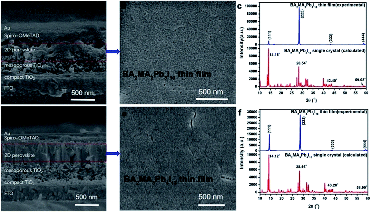 | ||
| Fig. 4 (a–f) The SEM images and XRD patterns of BA2MAn−1PbnI3n+1 (n = 3 and 4) films and solar cells based on their single crystal precursor by a modified hot-casting method. | ||
BA2MAn−1PbnI3n+1 (n = 3 and 4) solar cells with the structure of FTO/compact TiO2/mesoporous TiO2/BA2MAn−1PbnI3n+1 (n = 3 and 4)/spiro-OMeTAD/Au were fabricated and characterized under standard air-mass 1.5 global (AM 1.5G) illumination, as shown in Fig. 3(b) and 4(a and d). The J–V curves for the devices are presented in Fig. 5(a and d), which showed the important parameters of open-circuit voltage (Voc), short-circuit current density (Jsc), fill factor (FF) and PCE. In 2015, planar (BA)2(MA)2Pb3I10 solar cells based on similar architectural structures with the only maximum PCE of 4.02% were investigated by Cao et al.17 In our results, these devices presented relatively good photovoltaic performance. Maximum PCEs of 9.03% and 5.05% were obtained from the devices of BA2MA3Pb4I13 and (BA)2(MA)2Pb3I10 solar cells, respectively, due to the relatively higher Voc (976 mV and 986 mV) and Jsc (17.19 mA cm−2 and 11.3 mA cm−2) of the devices. These layered hybrid perovskites pave the way for achieving higher Voc, compared with 3D hybrid perovskite materials (Voc < 0.9).44–47Fig. 5(b and e) present the PCE distribution histogram of ∼100 solar cell devices based on BA2MAn−1PbnI3n+1 (n = 3 and 4, respectively), which exhibited the average PCEs of ∼4.5% and ∼8.0%, respectively. In Fig. 5(c and f), when the test voltage was fixed at 0.59 V, as the delay time increased from 0 s to 100 s, the Jsc of the devices kept stable at ∼7.6 mA cm−2 and ∼15.1 mA cm−2 and their PCEs also kept stable at 4.5% and 8.83%, respectively, showing stable working performance. Further enhancements of device performance may be achieved through the improvement in the quality of thin films, device structures, interfaces and electrodes. These results show that layered perovskite devices are stable when exposed to air and light irradiation conditions, which provides the possibility of further studies of optoelectronic devices based on layered perovskite single-crystalline materials.
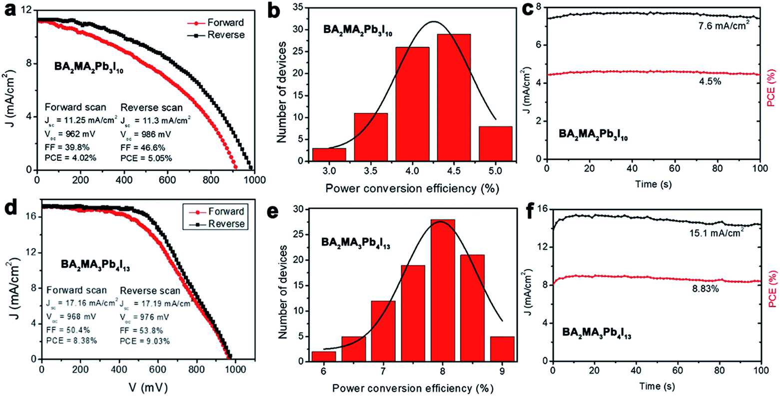 | ||
| Fig. 5 (a and d) The current-density–voltage (J–V) curves under an AM 1.5G solar simulator for BA2MAn−1PbnI3n+1 (n = 3 and 4) solar cell devices. (b and e) Device PCE histogram of BA2MAn−1PbnI3n+1 (n = 3 and 4) over 100 measured devices, fitted with a Gaussian distribution (black line). (c and f) Stability measurements on the solar cells based on BA2MAn−1PbnI3n+1 (n = 3 and 4) films. | ||
Conclusions
In summary, based on a strategy of decreasing the dimensionality and improving the stability of MAPbI3 hybrid perovskites, we report the bulk growth and solar cell investigations of layered 2D hybrid perovskite single crystals of BA2MAn−1PbnI3n+1 (n = 3 and 4). We show that the band gap and PL spectra can be tuned via the compositional concentration of small MA molecules. Of importance, the formation processes of BA2MAn−1PbnI3n+1 thin films based on their single-crystalline precursors by a modified hot-casting method were demonstrated for the first time. And the solar cells based on BA2MAn−1PbnI3n+1 (n = 3 and 4) single-crystalline precursor solutions showed good feasibility and stability, and exhibited higher PCEs of 5.05% and 9.03% (with the increase of the number of perovskite layers (n)), compared with the previously reported similar architectural structures based on these layered perovskite materials. Further enhancements of device performance may be achieved through amelioration of the quality of thin films, device structures and electrodes. This work provides an insightful understanding on the fundamental properties and thin film fabrication of these materials and frames a useful guide to achieve high performance optoelectronic devices based on emerging 2D perovskite monocrystalline materials.Experimental
Reagents
All starting reagents of PbO, CH3NH2, n-C4H9NH2, H3PO2 solution, 2-propanol, DMF, chlorobenzene and HI solution were of analytical grade from Sino-pharm Co. Ltd. and without further purification.Syntheses and crystal growth
The syntheses of MAI, n-C4H9NH3I and crystal growth were performed according to previously reported methods.29–34 But the synthesis of n-C4H9NH3I was based on the reaction of n-C4H9NH2 and HI in an ice bath in an ambient atmosphere. The white BAI in Fig. S2a† was obtained using a rotary evaporator and then dried at 60 °C at 24 h in air. The newly synthesized BAI (12.060 g, 0.06 mol) and PbO (6.696 g, 0.03 mol) were dissolved in a 200 ml HI and 50 ml H3PO2 mixed solution at 75 °C under constant stirring, forming a yellow transparent solution. Solutions were saturated at 60 °C. Orange layered BA2PbI4 single crystals have been grown by the top-seeded solution growth (TSSG) method in an ambient atmosphere for about two weeks, as shown in Fig. S1.†The newly synthesized BAI (12.060 g, 0.06 mol), MAI (11.925 g, 0.075 mol) and PbO (20.088 g, 0.09 mol) were dissolved in 250 ml HI solution at 65 °C under constant stirring, forming a yellow transparent solution. Solutions were saturated at 60 °C. Dark red plate and block BA2MA2Pb3I10 single crystals have been grown via different seed direction by the top-seeded solution growth (TSSG) method in an ambient atmosphere for about two weeks, as shown in Fig. 1(a and b).
The newly synthesized BAI (12.060 g, 0.06 mol), MAI (16.700 g, 0.105 mol) and PbO (26.784 g, 0.12 mol) were dissolved in 300 ml HI solution at 65 °C under constant stirring, forming a yellow transparent solution. Solutions were saturated at 55 °C. Black plate and block BA2MA3Pb4I13 single crystals have been grown with the different seed direction by the top-seeded solution growth (TSSG) method in an ambient atmosphere for about two weeks, as shown in Fig. 1(c and d).
Fabrication and measurement of BA2MAn−1PbnI3n+1 (n = 3 and 4) solar cell devices
FTO glasses were cleaned using an ultra-sonication bath in soap water and rinsed progressively with distilled water and isopropyl alcohol, and finally treated with oxygen plasma for 1 min. A thin blocking-TiO2 layer is first deposited onto fluorine doped tin oxide (FTO) by spin coating titanium diisopropoxide bis(acetylacetonate) solution (75% in 2-propanol) diluted in ethanol (1:15, volume ratio) and annealed at 500 °C for 30 min, followed by cooling to room temperature naturally. The mesoporous TiO2 layer composed of 20 nm-sized particles was deposited by spinning coating TiO2 paste (Dyesol 18NRT, Dyesol) diluted in ethanol (1:3.5 wt) at 1500 rpm. After drying at 125 °C, the TiO2 films were heated to 500 °C, baked at this temperature for 30 min and cooled to room temperature. Before use, the substrates were preheated to 130 °C.
The layered perovskite BA2MAn−1PbnI3n+1 (n = 3 and 4) precursor solution was prepared by dissolving 0.24 M perovskite single crystals in DMF. To get the perovskite film, the preheated FTO/TiO2 substrates were immediately transferred to the spin-coated pallet (which is at room temperature), and 60 μl of precursor solution was dropped onto the hot substrate. The spin-coater was immediately started with a spinning speed of 3500 rpm for 20 s. Chlorobenzene (200 μl) was dropped onto the spinning substrate at 10 s before the end of the procedure. After the spin-coater stopped, the substrates were quickly removed from it. The substrate was dried on a hot plate at 130 °C for 10 min.
Then the hole transporting material (HTM) was deposited by spin coating the solution of the HTM at 3000 rpm for 60 s. The HTM formulation was prepared by dissolving 2,2′,7,7′-tetrakis(N,N-p-dimethoxy-phenylamino)-9,9′-spirobifluorene (spiro-OMeTAD, 73 mg, Youxuan Tech Co. Ltd.), 4-tert-butylpyridine (tBP, 29.5 μl) and a stock solution of lithium bis(trifluoromethylsulphonyl)imide (Li-TFSI, 520 mg ml−1) in acetonitrile (18.5 μl) in 1 ml chlorobenzene. Finally, 80 nm gold electrodes were deposited on top of the devices by evaporation at ∼10−4 Pa.
The J–V characteristics were obtained using an Agilent B2900 Series precision source/measure unit, and the cell was illuminated with a solar simulator (Solar IV-150A, Zolix) under AM 1.5 irradiation (100 mW cm−2). The light intensity was calibrated with a Newport calibrated KG5-filtered Si reference cell. The masked active area was 0.1 cm2. J–V characteristics were obtained using curves recorded from 0.1 V to 1.2 V in the forward and reverse directions with a scanning velocity of 200 mV s−1. For stability measurements, the voltage was fixed at the maximum power point to test the current output for all the test time. The masked active area was 0.1 cm2.
Characterization
Single-crystal and powder X-ray diffraction, film X-ray diffraction, TGA/DSC, SEM, PL spectra, and UV-vis spectra measurements and fabrication of FASnI3 solar cells are described in detail in the ESI.†Conflicts of interest
There are no conflicts to declare.Acknowledgements
Dr Y. Dang and Dr J. Wei contributed equally to this work. This work is supported by the National Natural Science Foundation of China (grant no. 51321091), the National Key Research and Development Program of China (Grant No. 2016YFB1102201) and the 111 Project 2.0 (Grant No. BP2018013). Dr Y. Dang and Dr J. Wei acknowledge the Project funded by the China Postdoctoral Science Foundation (No. 2017M621067, 2018T110197 and 2017M620694), respectively. Dr J. Wei acknowledges the National Postdoctoral Program for Innovative Talents (BX201700040). All the authors greatly thank Qingming Lu, Zhongjun Zhai, and Xiufeng Cheng for their help in measurements of crystal orientation, crystal processing and thermal properties, respectively, and also greatly thank Prof. Hong-Zheng Chen and Dr Wei-Fei Fu, Zhejiang University for their help in the fabrication and measurement of FASnI3 solar cells.Notes and references
- D. Shi, V. Adinolfi, R. Comin, M. Yuan, E. Alarousu, A. Buin, Y. Chen, S. Hoogland, A. Rothenberger, K. Katsiev, Y. Losovyj, X. Zhang, P. A. Dowben, O. F. Mohammed, E. H. Sargent and O. M. Bakr, Science, 2015, 347, 519 CrossRef PubMed.
- (a) X. Chin, D. Cortecchia, J. Yin, A. Bruno and C. Soci, Nat. Commun., 2015, 6, 7383 CrossRef PubMed; (b) X. Zhang, S. Bi, J. Zhou, S. You, H. Zhou, Y. Zhang and Z. Tang, J. Mater. Chem. C, 2017, 5, 9376 RSC.
- Q. Dong, Y. Fang, Y. Shao, P. Mulligan, J. Qiu, L. Cao and J. Huang, Science, 2015, 347, 967 CrossRef PubMed.
- N. Onoda-Yamamuro, T. Matsuo and H. Suga, J. Phys. Chem. Solids, 1990, 51, 1383 CrossRef.
- (a) X. Qin, H. Dong and W. Hu, Sci. China Mater., 2015, 58, 186 CrossRef; (b) D. B. Mitzi, Chem. Mater., 1997, 9, 2990 CrossRef.
- (a) W. Liao, Y. Zhang, C. Hu, J. Mao, H. Ye, P. Li, S. Huang and R.-G. Xiong, Nat. Commun., 2015, 6, 7338 CrossRef PubMed; (b) Y. You, W.-Q. Liao, D. Zhao, H.-Y. Ye, Y. Zhang, Q. Zhou, X. Niu, J. Wang, P. F. Li, D. W. Fu, Z. Wang, S. Gao, K. Yang, J. M. Liu, J. Li, Y. Yan and R.-G. Xiong, Science, 2017, 357, 306 CrossRef PubMed.
- (a) H. S. Kim, S. K. Kim, B. J. Kim, K. S. Shin, M. K. Gupta, H. S. Jung, S. W. Kim and N. G. Park, J. Phys. Chem. Lett., 2015, 6, 1729 CrossRef PubMed; (b) J. Wei, Y. Zhao, H. Li, G. Li, J. Pan, D. Xu, Q. Zhao and D. Yu, J. Phys. Chem. Lett., 2014, 5, 3937 CrossRef PubMed.
- C. C. Stoumpos, C. D. Malliakas and M. G. Kanatzidis, Inorg. Chem., 2013, 52, 9019 CrossRef PubMed.
- Y. Kutes, L. Ye, Y. Zhou, S. Pang, B. D. Huey and N. P. Padture, J. Phys. Chem. Lett., 2014, 5, 3335 CrossRef PubMed.
- S. Liu, F. Zheng, N. Z. Koocher, H. Takenaka, F. Wang and A. M. Rappe, J. Phys. Chem. Lett., 2015, 6, 693 CrossRef PubMed.
- X. Mettan, R. Pisoni, P. Matus, A. Pisoni, J. Jaćimović, B. Náfrádi, M. Spina, D. Pavuna, L. Forró and E. Horváth, J. Phys. Chem. C, 2015, 119, 11506 CrossRef.
- A. Pisoni, J. Jaćimović, O. S. Barišić, M. Spina, R. Gaál, L. Forró and E. Horváth, J. Phys. Chem. Lett., 2014, 5, 2488 CrossRef PubMed.
- (a) C. K. Moller, Nature, 1958, 182, 1436 CrossRef; (b) G. Maculan, A. D. Sheikh, A. L. Abdelhady, M. I. Saidaminov, M. A. Haque, B. Murali, E. Alarousu, O. F. Mohammed, T. Wu and O. M. Bakr, J. Phys. Chem. Lett., 2015, 6, 3781 CrossRef PubMed; (c) Y. Fang, Q. Dong, Y. Shao, Y. Yuan and J. Huang, Nat. Photonics, 2015, 9, 679 CrossRef.
- (a) J. Shi, X. Xu, D. Li and Q. Meng, Small, 2015, 11, 2472 CrossRef PubMed; (b) Y. Wang, S. Bai, L. Cheng, N. Wang, J. Wang, F. Gao and W. Huang, Adv. Mater., 2016, 28, 4532 CrossRef PubMed; (c) D. Zhao, Y. Yu, C. Wang, W. Liao, N. Shrestha, C. R. Grice, A. J. Cimaroli, L. Guan, R. J. Ellingson, K. Zhu, X. Zhao, R.-G. Xiong and Y. Yan, Nat. Energy, 2017, 2, 17018 CrossRef; (d) K. Wang, C. Liu, P. Du, J. Zheng and X. Gong, Energy Environ. Sci., 2015, 8, 1245 RSC.
- A. Kojima, K. Teshima, Y. Shirai and T. Miyasaka, J. Am. Chem. Soc., 2009, 131, 6050 CrossRef PubMed.
- National Renewable Energy Labs (NREL) Efficiency Chart, 2018, https://www.nrel.gov/ncpv/images/efficiency_chart.jpg.
- D. H. Cao, C. C. Stoumpos, O. K. Farha, J. T. Hupp and M. G. Kanatzidis, J. Am. Chem. Soc., 2015, 137, 7843 CrossRef PubMed.
- D. B. Mitzi, C. A. Field, W. T. A. Harrison and A. M. Guloy, Nature, 1994, 369, 467 CrossRef.
- C. C. Stoumpos, D. H. Cao, D. J. Clark, J. Young, J. M. Rondinelli, J. I. Jang, J. T. Hupp and M. G. Kanatzidis, Chem. Mater., 2016, 28, 2852 CrossRef.
- H. Tsai, W. Nie, J. C. Blancon, C. C. Stoumpos, R. Asadpour, B. Harutyunyan, A. J. Neukirch, R. Verduzco, J. J. Crochet, S. Tretiak, L. Pedesseau, J. Even, M. A. Alam, G. Gupta, P. M. Ajayan, M. J. Bedzyk, M. G. Kanatzidis and A. D. Mohite, Nature, 2016, 536, 312 CrossRef PubMed.
- (a) I. C. Smith, E. T. Hoke, D. Solis-Ibarra, M. D. McGehee and H. I. Karunadasa, Angew. Chem., Int. Ed., 2014, 53, 11232 CrossRef PubMed; (b) C. C. Chueh, C.-Z. Li and A. K.-Y. Jen, Energy Environ. Sci., 2015, 8, 1160 RSC.
- C. R. Kagan, D. B. Mitzi and C. D. Dimitrakopoulos, Science, 1999, 286, 945 CrossRef PubMed.
- (a) X. X. Wu, M. T. Trinh, D. Niesner, H. M. Zhu, Z. Norman, J. S. Owen, O. Yaffe, B. J. Kudisch and X. Y. Zhu, J. Am. Chem. Soc., 2015, 137, 2089 CrossRef PubMed; (b) J. Wang, N. Wang, Y. Jin, J. Si, Z. Tan, H. Du, L. Cheng, X. Dai, S. Bai, H. He, Z. Ye, M. Lai, R. H. Friend and W. Huang, Adv. Mater., 2015, 27, 2311 CrossRef PubMed; (c) M. Yuan, L. Quan, R. Comin, G. Walters, R. Sabatini, O. Voznyy, S. Hoogland, Y. Zhao, E. M. Beauregard, P. Kanjanaboos, Z. Lu, D. H. Kim and E. H. Sargent, Nat. Nanotechnol., 2016, 11, 872 CrossRef PubMed.
- A. Bravais, Etudes Cristal-géographiques, Academie des Sciences, Paris, 1913 Search PubMed.
- C. F. Macrae, P. R. Edgington, P. McCabe, E. Pidcock, G. P. Shields, R. Taylor, M. Towler and J. Van de Streek, J. Appl. Crystallogr., 2006, 39, 453 CrossRef.
- Summary of crystal data: (a) BA2PbI4, orange platelet; empirical formula: C8H24N2PbI4; crystal system: orthorhombic; space group: Pbca, at 293 K; a =8.892 Å, b = 8.713 Å, c = 27.650 Å, V = 2142.30 Å3, Z = 4; (b) BA2MA2Pb3I10, dark-red platelet; empirical formula: C10H36N4Pb3I10; crystal system: orthorhombic; space group: Cmca at 293 K; a =8.886 Å, b = 51.942 Å, c = 8.919 Å, V = 4116.46 Å3, Z = 4; (c) BA2MA3Pb4I13, black platelet; empirical formula: C11H42N5Pb4I13; crystal system: orthorhombic; space group: Ccmm at 293 K; a = 8.976 Å, b = 64.499 Å, c = 8.941Å, V = 5176.23 Å3, Z = 4.
- D. G. Billing and A. Lemmerer, Acta Crystallogr., Sect. B: Struct. Sci., 2007, 63, 735 CrossRef PubMed.
- D. B. Mitzi, Chem. Mater., 1996, 8, 791 CrossRef.
- Y. Dang, Y. Liu, Y. Sun, D. Yuan, X. Liu, W. Lu, G. Liu, H. Xia and X. Tao, CrystEngComm, 2015, 17, 665 RSC.
- Y. Dang, Y. Zhou, X. Liu, D. Ju, S. Xia, H. Xia and X. Tao, Angew. Chem., Int. Ed., 2016, 55, 3447 CrossRef PubMed.
- Y. Dang, C. Zhong, G. Zhang, D. Ju, L. Wang, S. Xia, H. Xia and X. Tao, Chem. Mater., 2016, 28, 6968 CrossRef.
- D. Ju, T. Zhao, Y. Dang, G. Zhang, X. Hu, D. Cui and X. Tao, J. Mater. Chem. A, 2017, 5, 21919 RSC.
- Y. Dang, X. Meng, K. Jiang, C. Zhong, X. Chen and J. Qin, Dalton Trans., 2013, 42, 9893 RSC.
- D. Ju, Y. Dang, Z. Zhu, H. Liu, C. C. Chueh, X. Li, L. Wang, X. Hu, A. K.-Y. Jen and X. Tao, Chem. Mater., 2018, 30, 1556 CrossRef.
- J. C. Blancon, H. Tsai, W. Nie, C. C. Stoumpos, L. Pedesseau, C. Katan, M. Kepenekian, C. M. M. Soe, K. Appavoo, M. Y. Sfeir, S. Tretiak, P. M. Ajayan, M. G. Kanatzidis, J. Even, J. J. Crochet and A. D. Mohite, Science, 2017, 355, 1288 CrossRef PubMed.
- F. Hao, C. C. Stoumpos, Z. Liu, R. P. H. Chang and M. G. Kanatzidis, J. Am. Chem. Soc., 2014, 136, 16411 CrossRef PubMed.
- Y. Rong, Z. Tang, Y. Zhao, X. Zhong, S. Venkatesan, H. Graham, M. Patton, Y. Jing, A. M. Guloy and Y. Yao, Nanoscale, 2015, 7, 10595 RSC.
- M. Xiao, F. Huang, W. Huang, Y. Dkhissi, Y. Zhu, J. Etheridge, A. Gray Weale, U. Bach, Y. B. Cheng and L. Spiccia, Angew. Chem., 2014, 126, 10056 CrossRef.
- D. Shen, X. Yu, X. Cai, M. Peng, Y. Ma, X. Su, L. Xiao and D. Zou, J. Mater. Chem. A, 2014, 2, 20454 RSC.
- Y. Dang, D. Ju, L. Wang and X. Tao, CrystEngComm, 2016, 18, 4476 RSC.
- Y. Guo, K. Shoyama, W. Sato, Y. Matsuo, K. Inoue, K. Harano, C. Liu, H. Tanaka and E. Nakamura, J. Am. Chem. Soc., 2015, 137, 15907 CrossRef PubMed.
- Y. Zhao, J. Wei, H. Li, Y. Yan, W. Zhou, D. Yu and Q. Zhao, Nat. Commun., 2016, 7, 10228 CrossRef PubMed.
- J. Wei, H. Li, Y. Zhao, W. Zhou, R. Fu, Y. Leprince-Wang, D. Yu and Q. Zhao, Nano Energy, 2016, 26, 139 CrossRef.
- T. Leijtens, G. E. Eperon, S. Pathak, A. Abate, M. M. Lee and H. J. Snaith, Nat. Commun., 2013, 4, 2885 CrossRef PubMed.
- W. Nie, H. Tsai, R. Asadpour, J. C. Blancon, A. J. Neukirch, G. Gupta, J. J. Crochet, M. Chhowalla, S. Tretiak, M. A. Alam, H.-L. Wang and A. D. Mohite, Science, 2015, 347, 522 CrossRef PubMed.
- P. W. Liang, C. Y. Liao, C. C. Chueh, F. Zuo, S. T. Williams, X. K. Xin, J. Lin and A. K. Y. Jen, Adv. Mater., 2014, 26, 3748 CrossRef PubMed.
- Y. J. Jeon, S. Lee, R. Kang, J. E. Kim, J. S. Yeo, S. H. Lee, S. S. Kim, J. M. Yun and D. Y. Kim, Sci. Rep., 2014, 4, 6953 CrossRef PubMed.
Footnotes |
| † Electronic supplementary information (ESI) available. See DOI: 10.1039/c8se00213d |
| ‡ The authors contributed equally to this work. |
| This journal is © The Royal Society of Chemistry 2018 |