
Critical role of {002} preferred orientation on electronic band structure of electrodeposited monoclinic WO3 thin films†
Wai Ling
Kwong
 ab,
Pramod
Koshy
a,
Judy N.
Hart
a,
Wanqiang
Xu
a and
Charles C.
Sorrell
*a
ab,
Pramod
Koshy
a,
Judy N.
Hart
a,
Wanqiang
Xu
a and
Charles C.
Sorrell
*a
aSchool of Materials Science and Engineering, UNSW Sydney, NSW 2052, Australia. E-mail: C.Sorrell@unsw.edu.au; Fax: +61-2-9385-6565; Tel: +61-2-9385-4421
bNow at Department of Chemistry-Ångström Laboratory, Molecular Biomimetics, Uppsala University, S-75120 Uppsala, Sweden
First published on 4th September 2018
Abstract
Monoclinic WO3 films with tunable (002) and (200) orientations parallel to fluorine-doped tin oxide substrates were electrodeposited from peroxotungstic acid (PTA) solutions and subjected to annealing (≤500 °C). It is concluded that the crystallographic orientations of the films are dependent on the nucleation density and the thermal-induced recrystallisation kinetics, which can be controlled respectively by the tungsten concentration of the PTA solution and the annealing conditions. This approach allows the fabrication of films with preferred (002), equally mixed (002) and (200), and (200) orientations, which were characterised in terms of the associated mineralogical, nanostructural, optical, chemical, photoelectrochemical, and photocatalytic properties. The present work decouples the concurrent effects of crystallographic orientation and trend in oxygen vacancy concentration on the optical indirect band gap of WO3 thin films, where the linear correlation between these three variables can be used as a diagnostic tool to engineer the electronic band structure of films for applications requiring photosensitivities in different regions of the solar spectrum. In effect, a low valence band maximum, low oxygen vacancy concentration, and resultant low band gap associated with (002) preferred orientation results in the highest photoelectrochemical performance, which is relevant to applications under solar illumination. In contrast, a high concentration of oxygen vacancies, which act as surface reaction sites associated with (200) preferred orientation, results in the highest efficiency in the photodegradation of methylene blue, which is relevant to applications under UV illumination.
1. Introduction
Preferred crystallographic orientation and associated differential properties result from anisotropic crystal growth in specific directions. For example, microstructures of the wurtzite polymorph of ZnO with (10![[1 with combining macron]](https://www.rsc.org/images/entities/char_0031_0304.gif) 0) orientation demonstrate superior photocatalytic efficiency in degrading methylene blue to those with (0001) orientation owing to the presence of oxygen vacancies on the (100) plane, which creates midgap states and so enhances the photosensitivity in the visible region.1 The anatase polymorph of TiO2 with predominantly (001) orientation demonstrates enhanced photocatalytic production of hydroxyl radicals compared to that of reference TiO2 without preferred orientation owing to the unique electronic structure of the unsaturated fivefold Ti in the terminating (001) plane.2 Another recent study reported that, by eliminating the (101) orientation during crystal growth of plate-like grains, the resultant anatase could be made more reactive.3 That is, both the (001) and (100) planes show improved photocatalytic properties in terms of hydroxyl radical production and degradation of methyl orange compared to the less reactive (101) plane. The preceding examples show that the photocatalytic performances of materials, which are determined by their physical and electronic properties, can be strongly dependent on the crystallographic orientations of the exposed surfaces. Therefore, it is important to understand and control the crystallography of a material for optimisation of its properties.
0) orientation demonstrate superior photocatalytic efficiency in degrading methylene blue to those with (0001) orientation owing to the presence of oxygen vacancies on the (100) plane, which creates midgap states and so enhances the photosensitivity in the visible region.1 The anatase polymorph of TiO2 with predominantly (001) orientation demonstrates enhanced photocatalytic production of hydroxyl radicals compared to that of reference TiO2 without preferred orientation owing to the unique electronic structure of the unsaturated fivefold Ti in the terminating (001) plane.2 Another recent study reported that, by eliminating the (101) orientation during crystal growth of plate-like grains, the resultant anatase could be made more reactive.3 That is, both the (001) and (100) planes show improved photocatalytic properties in terms of hydroxyl radical production and degradation of methyl orange compared to the less reactive (101) plane. The preceding examples show that the photocatalytic performances of materials, which are determined by their physical and electronic properties, can be strongly dependent on the crystallographic orientations of the exposed surfaces. Therefore, it is important to understand and control the crystallography of a material for optimisation of its properties.
Photoelectrochemical production of molecular hydrogen (H2) is an environmentally neutral and sustainable energy-harvesting method whereby H2 fuel is produced by the photolysis of water.4 The surface state of a photoelectrode has a critical effect on the efficiency of a photoelectrochemical cell.5,6 It accommodates water oxidation (in the case of an n-type photoanode) at the photoanode/electrolyte interface. This interfacial reaction is influenced by the (i) surface configuration (numbers of reaction and recombination sites), which determines the efficiencies of photogenerated hole transport and the adsorption of reactants (water molecules) at the interface, and (ii) surface electronic states (valence and conduction band edges), which determine the reduction and oxidation potentials of the photogenerated electrons and holes, respectively, and thus the feasibility of reduction and oxidation of water molecules by these charge carriers.7 The anisotropic properties associated with different crystallographic planes of a material indicate that the crystallographic orientation of a photoelectrode surface can influence its photoelectrochemical performance.
Tungsten oxide (WO3) is an n-type semiconductor with an indirect optical band gap of ∼2.7 eV.8,9 The monoclinic γ polymorph is the stable phase in the temperature range 17–330 °C.10 Randomly distributed monoclinic WO3 powders show equivalent intensities for the X-ray diffraction peaks of the three dominant planes (002), (020), and (200).11 WO3 has a high potential to serve as a photoanode for water splitting due to its adequate photoelectrochemical performance in acidic solutions and its photosensitivity to visible light.12 Recent studies have shown that the growth of WO3 grain facets can be controlled through the use of growth-directing agents,7,13–17 which are adsorbed preferentially on the crystal surfaces. The monoclinic WO3 quasi-cubic-like crystals, with equal proportions of (002), (020), and (200) facets, show superior water oxidation activity compared to rectangular sheet-like samples with predominantly (002) facets owing to the lower valence band maximum and hence stronger oxidising power of the former.7 Nonetheless, the latter is more effective in the photocatalytic reduction of CO2 owing to its higher conduction band minimum, which results in a higher reduction potential of the photogenerated electrons. Zhang et al.14 produced orthorhombic WO3 nanocrystals with tunable (001) facet surface area and observed that the high-surface-energy (001) facet demonstrated the best photocatalytic activity owing to enhanced photoexcitation and suppressed charge carrier recombination.
While most studies have focused on growth control of the typically exposed {001} crystal facets of WO3 powders,7,13–18 equivalent work in the fabrication of thin films for use in photoelectrochemical cells is uncommon. Further, the use of growth-directing agents has the potential to result in sample contamination. The present work demonstrates a novel approach to control the crystallographic {002} orientations of electrodeposited monoclinic WO3 thin films uncontaminated by growth-directing agents through the manipulation of the deposition and annealing parameters. That is, the crystallographic growth of the films is controlled by varying the tungsten concentration of the peroxotungstic acid (PTA) precursor and the post-deposition annealing temperature and time. It is shown for the first time that decoupling the concurrent effects of the dominant crystallographic orientation and the trend of the oxygen vacancy concentration on the optical indirect band gap of WO3 thin film offers a means of engineering the electronic band structure of films.
2. Experimental details
2.1 Synthesis of WO3 films
Detailed procedures for the preparation of peroxotungstic acid (PTA) solutions have been reported elsewhere.19 Briefly, the PTA solutions, which served as the deposition electrolyte, contained 0.05–0.20 mol L−1 tungsten. In the previous work,19 the films deposited from PTA solutions containing this range of tungsten concentrations were observed to exhibit different crystallographic orientations. Tungsten oxide thin films were electrodeposited at room temperature using an electrochemical cell consisting of a computer-controlled potentiostat connected to a substrate of fluorine-doped tin oxide on glass (FTO), platinum (Pt) foil, and Ag/AgCl as the working, counter, and reference electrodes, respectively. All potentials reported refer to the reference electrode. A deposition potential of −0.4 V was applied. A longer time of 3 h was used for the deposition from PTA consisting of 0.05 mol L−1 tungsten as opposed to a shorter time of 0.5 h for 0.20 mol L−1 tungsten in order to fabricate films of uniform thicknesses (650 ± 8 nm) since the deposition rate was lower for PTA solutions with lower tungsten concentrations. The as-deposited films were flushed immediately with distilled water, dried in air, placed on an aluminosilicate brick, and annealed at 250–500 °C in air for times in the range 0.5–18.0 h (heating and initial cooling rates were 5 °C min−1).2.2 Characterisation
The mineralogies of the films were determined by X-ray powder diffraction (XRD; PANalytical X'pert multipurpose X-ray diffractometer; Bragg–Brentano configuration; CuKα radiation; 45 kV; 40 mA; step size 0.026° 2θ; scan speed 0.22° 2θ s−1). Normalised pole figures of the surfaces of the films were obtained using a Philips X'pert MRD system (step size of 3° 2θ). The software PANalytical X'pert HighScore Plus was used to analyse the XRD spectra. Nanostructural examination was done using scanning electron microscopy (SEM; FEI Nova NanoSEM; uncoated samples; accelerating voltage 5 kV), transmission electron microscopy (TEM; Phillips CM200; Pt- and Au-coated samples; accelerating voltage 200 kV), and atomic force microscopy (AFM; Bruker Dimension Icon; tapping mode). The film thicknesses were determined using focused ion beam milling (FIB; FEI XP200; Pt-coated samples; 30 keV Ga ions). Light transmission was measured using a dual-beam UV-visible spectrophotometer (Perkin-Elmer Lambda 35). Surface elemental composition and electronic valence band spectra were examined using X-ray photoelectron spectroscopy (XPS; Thermo Scientific Escalab 250; 150 W monochromated AlKα X-ray source with spot size of 500 μm), where the pass energies for survey and region scans were 100 eV and 20 eV, respectively. The software Advantage was used to analyse the XPS spectra. The binding energies were referenced to carbon (1s) from adventitious hydrocarbon at 285 eV.2.3 Photoelectrochemical and photocatalytic evaluation
The photoelectrochemical properties of the samples were measured at room temperature using the same electrochemical system as described above, with a WO3 thin film on FTO substrate and 0.5 mol L−1 NaCl aqueous solution (pH = 6.27) as the working electrode and electrolyte solution, respectively. A solar simulator equipped with a 300 W ozone-free Xe arc lamp (Newport 6258) was used as the light source. The solar simulator was coupled with air mass 1.5 global (Newport 81094) and UV blocking (<305 nm; Newport 20CGA-305) filters. The light intensity was measured using a light power meter (Thorlabs PM100USB) equipped with a thermal power sensor (Thorlabs S314C) to be ∼280 mW cm−2 (light source to sample distance ∼9.5 cm). The linear potentiodynamic photocurrent densities were measured at a scan rate of 5 mV s−1 with a step size of 1 mV. Cyclic voltammetry of the films involved scanning from −0.5 V to +0.5 V at a rate and step size of 5 mV s−1 and 1 mV, respectively, in dark environment.The photocatalytic activities of the films (area 1.5 × 1.5 cm) were determined by the photodegradation of methylene blue. Prior to the start of the measurement, each film was immersed for ∼24 h in a methylene blue aqueous solution of concentration 1 ppm or 4.5 ppm in order to achieve surface absorption equilibrium. Each film then was placed in 20 mL of methylene blue solution of corresponding concentration, contained in a 50 mL Pyrex beaker, and illuminated at a sample-lamp distance of 10 cm for 0–23 h using an 8 W Hg lamp (UVP; major spectral output at 254 nm or 365 nm). The resultant methylene blue solutions were taken at specific irradiation time intervals for the measurement of optical absorption spectra using the UV-visible spectrophotometer. The intensities of the characteristic absorption peaks of methylene blue at ∼664 nm were recorded for the evaluation of the photodegradation performance using the Beer–Lambert equation:20,21A = ε × l × C, where A, ε, l, and C are the optical absorbance, molar absorptivity, optical path length, and concentration (at irradiation time t) of the methylene blue solution, respectively. Since ε and l are constant, the absorbance is linearly proportional to the concentration of methylene blue in the solution. The performances of the films for the photocatalytic degradation of methylene blue were evaluated from the relative concentrations of methylene blue with respect to the initial concentration (at t = 0) as a function of irradiation time. A control sample (methylene blue solution containing no film) also was examined for comparative purposes.
3. Results and discussion
3.1 Films deposited from PTA solution of high tungsten concentration (0.20 mol L−1)
Films deposited from PTA containing 0.20 mol L−1 tungsten were heat treated at various conditions in order to study the effect of the annealing process on the crystallographic development of the films. Fig. 1 shows the X-ray diffraction (XRD) spectra of the films annealed at 25–500 °C for 0.5 h. The as-deposited film and the film annealed at 250 °C are amorphous, as indicated by the absence of WO3 peaks. The films began to recrystallise at ∼275 °C. The crystalline films are monoclinic, with dominant (002), (020), and (200) planes at 23.1°, 23.6°, and 24.3° 2θ, respectively.11 In addition to the increasing peak intensities with increasing annealing temperature, preferred crystallographic growth parallel to the substrate also is observed, where the (200) peak intensity increases more than that of (002) but the (020) peak intensity remains fairly constant. The mirror plane perpendicular to the k axis is known to facilitate ion deposition in the [002] and [200] directions.11 Similar changes in the preferred crystallographic orientations with annealing temperature have been observed in electrochromic studies of electrodeposited WO3 films.22,23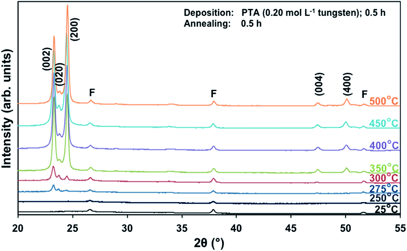 | ||
| Fig. 1 XRD spectra of the films deposited from PTA consisting of 0.20 mol L−1 tungsten and annealed for 0.5 h at temperatures 25–500 °C; F denotes peaks for FTO. | ||
The differences in the X-ray attenuation coefficients between these planes are considered irrelevant to the differences in the X-ray peak intensities observed in the present work because randomly oriented WO3 powders display almost equivalent intensities for the three dominant peaks from the (002), (020), and (200) planes,11,24 although the ionic population density of the (020) plane is greater than those of the (002) and (200) planes.25,26
In order to study the relationship between the predominance of the crystallographic planes parallel to the substrate and the annealing parameters (i.e., temperature and time), the relative intensity ratios (based on peak heights in the absence of a standard) R(x) = I(x)/(I(002) + I(020) + I(200)) (where (x) = (002), (020), or (200)) were determined from the XRD spectra in Fig. 1 and are shown in Fig. 2. The intensities of the peaks other than {002} in the present work are negligibly small and so have no significant influence on the values of R(x). Consideration of the standard XRD pattern for monoclinic WO3 (see Fig. 5) over the 2θ range of 20–25° indicates that the R(x) for each of the {002} planes in randomly distributed powders should be ∼0.33.11 The change in this ratio is a reflection of the competing growth rates of the crystal planes. The relative ratios calculated from the XRD peak intensities and peak areas are close (<10% difference).27
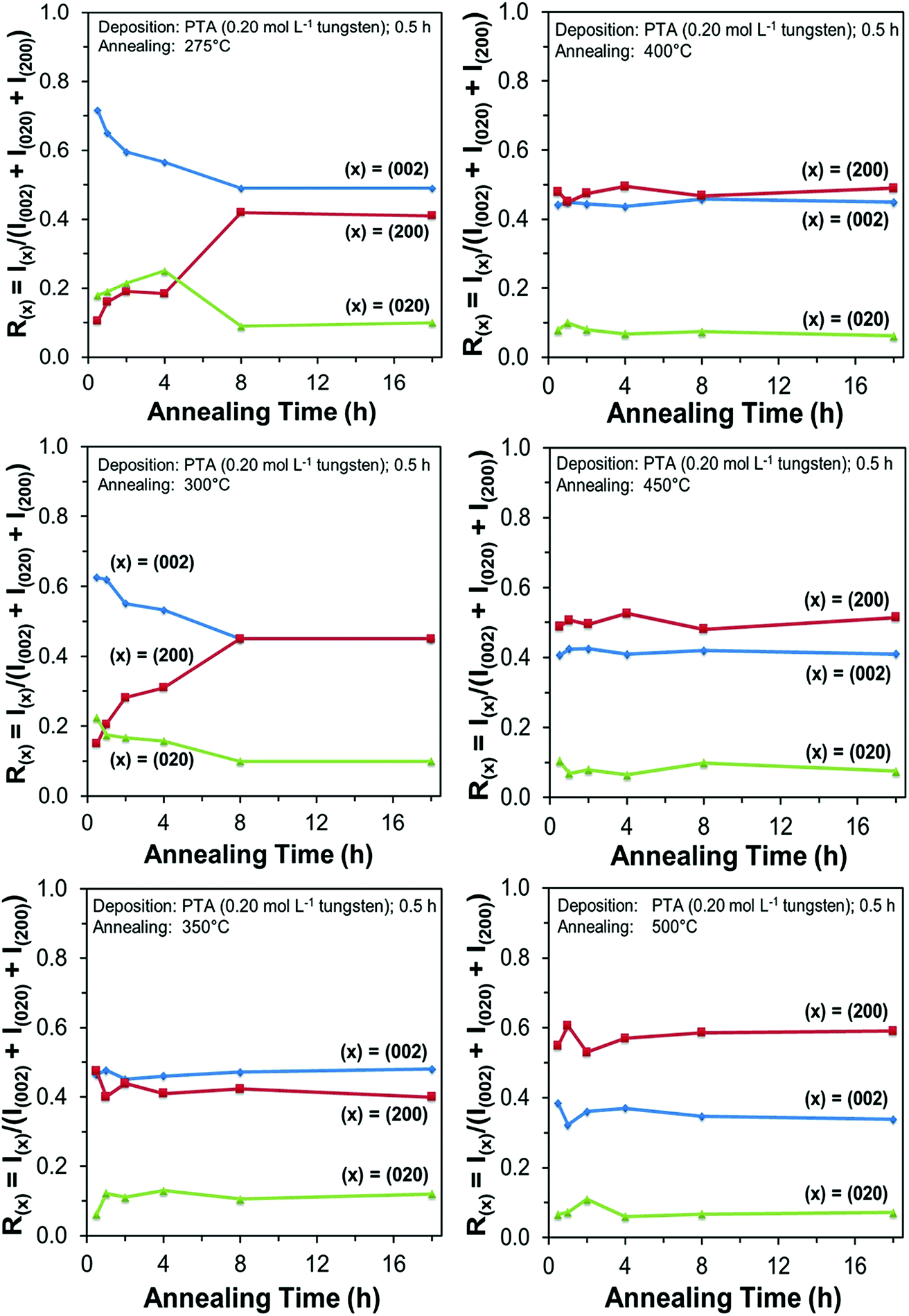 | ||
| Fig. 2 Relative XRD peak intensities Rx = I(x)/(I(002) + I(020) + I(200)) (where (x) = (002), (020), or (200)) as a function of annealing time for the films deposited from PTA consisting of 0.20 mol L−1 tungsten and annealed at temperatures in the range 275–500 °C. | ||
At the low annealing temperature of 275 °C, increasing the annealing time significantly increases the proportion of (200) plane largely at the expense of the (002) plane during the first 8 h of annealing, although the latter remains the principal plane parallel to the substrate of the films throughout the annealing period. At 300 °C, the R(002) and R(200) follow the same significant change in amount as at 275 °C during initial annealing but they equalise after 8 h. For these two low annealing temperatures, there is a slight decrease in the R(020). In contrast, at high annealing temperatures (≥350 °C), the R(x) values of all three planes change insignificantly as a function of time but the variations in the R(002) and R(200) as a function of temperature show a clear increasing trend in the latter at the expense of the former, while the R(020) remains approximately constant. These results indicate that, in general, the annealing temperature plays the dominant role in the development of preferred orientation through recrystallisation and grain growth while the annealing time has minimal impact.
The preceding data are quantified further in the bar charts shown in Fig. 3. Fig. 3(a) shows that, for the point of early recrystallisation at 0.5 h annealing, there are two temperature regions for the evolution of preferred orientation parallel to the substrate:
 | ||
| Fig. 3 Relative XRD peak intensities R(x) = I(x)/(I(002) + I(020) + I(200)) (where (x) = (002), (020), or (200)) as a function of annealing temperature for films deposited from PTA consisting of 0.20 mol L−1 tungsten and annealed for (a) 0.5 h or (b) 8 h. | ||
Low temperatures (<350 °C): Since R(002) is >0.33, then this indicates the predominance of the (002) plane. However, increasing the temperature within the low-temperature region enhances the relative growth rates of the (020) and (200) planes, thereby decreasing the R(002).
High temperatures (≥350 °C): Since R(002) and R(200) are >0.33, then this indicates the continued predominance of the (002) and (200) orientations. However, the latter gradually increases with increasing annealing temperature while the former decreases (and the (020) orientation remains low). The predominance of the (200) plane indicates that it is thermodynamically the most stable. This is emphasised by the results at 500 °C in Fig. 3, in which the R(200)/R(002) ratio after 8 h annealing shows the greatest differential compared to that after 0.5 h annealing. This conclusion is applicable provided there is no epitaxial growth, which is absent in the present work.
Fig. 3(b) shows that, for the point at which the rate of recrystallisation stabilises at 8 h annealing, both the R(002) and R(200) are >0.33, which indicate the predominance of these two orientations. The differential between the R(002) and R(200) at low temperatures is less significant than that of the early point (0.5 h annealing) of recrystallisation in Fig. 3(a). This is a reflection of the kinetics of recrystallisation, where the relatively greater R(200) levels in the low-temperature region at the longer annealing time of 8 h are reflections of the greater thermodynamic stability of the (200) plane compared to that of the (002) plane.
3.2 Films deposited from PTA solution of low tungsten concentration (0.05 mol L−1)
The effects of annealing temperature and time on the preferred orientation parallel to the substrate of the films also were investigated for films deposited from PTA containing the low tungsten concentration of 0.05 mol L−1. Fig. 4 shows the XRD spectra of the films annealed at different temperatures for 0.5 h. It can be seen that, in contrast to the results for high tungsten concentration in Fig. 1, the (002) plane is predominant at all annealing temperatures ≥350 °C. The R(x) trends, shown in Fig. S1 and S2,† confirm that the (002) plane remains predominant for the investigated ranges of annealing temperature and time. This is in contrast to the trends shown in Fig. 2 and 3 for the films deposited from PTA consisting of the higher tungsten concentration of 0.20 mol L−1, for which the preferred orientations changed from (002) to (200) with increasing annealing temperature.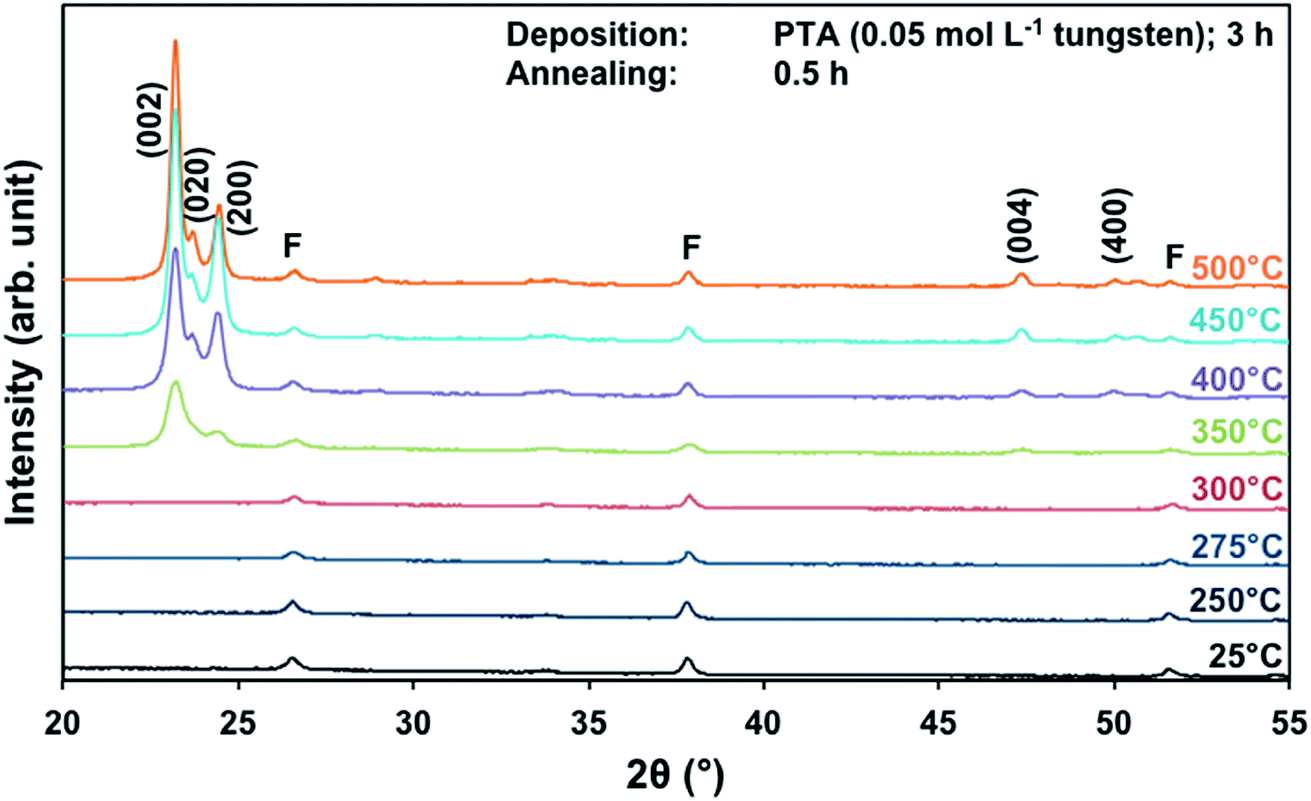 | ||
| Fig. 4 XRD spectra of the films deposited from PTA consisting of 0.05 mol L−1 tungsten and annealed for 0.5 h at 25–500 °C; F denotes peaks for FTO. | ||
These data suggest that the tungsten concentration of the PTA solution determines the homogeneity of the films and that this strongly affects the grain growth and associated development of preferred orientation during annealing. That is, depositions from PTA solutions consisting of low (0.05 mol L−1) and high (0.20 mol L−1) tungsten concentrations yield inhomogeneously and homogeneously nanostructured films, respectively. The XRD data for the films deposited from PTA solutions consisting of low tungsten concentration (Fig. 4, S1, and S2†), which have inhomogeneous nanostructures, indicate the following:
(i) A higher apparent onset recrystallisation temperature of >300 °C is required owing to the sparse nucleation distribution and small particle sizes; hence, a higher annealing temperature is required to activate recrystallisation, which allows the X-ray diffractometer to detect the larger sized grains.
(ii) The consistent predominance of the R(002) at all annealing temperatures and times indicates that the (002) plane is favoured for grain growth, where the large grains grow at the expense of adjacent smaller ones.
(iii) The absence of trend in the R(200)/R(002) ratio as a function of annealing temperature and time for annealing temperatures <500 °C indicates a greater hindrance of the growth of the thermodynamically stable (200) plane.
(iv) The requirement of higher annealing temperature (500 °C) and longer annealing time (∼8 h) to increase the R(200)/R(002) ratio further confirms the high thermodynamic stability of the (200) plane.
3.3 Mechanism of preferred crystallographic orientation in electrodeposited WO3 thin films
The surface energy of a thin-film system originates from the (i) film/atmosphere interface (ii) film/substrate interface, and (iii) intergranular interfaces. When an amorphous film recrystallises during annealing, the crystals that form reconfigure their surfaces by developing the crystal planes with low surface energy in order to minimise the total surface energy of the system.28 It has been reported that the surface energies per unit area of {002} planes of monoclinic WO3, based on density functional theory calculations,7,14,29 follow the order (002) > (020) > (200). A high surface energy is a reflection of the high reactivity and associated high growth rate of a crystal plane,30,31 which is associated with low thermodynamic stability (although grain growth is a parameter of transient-state kinetics, thermodynamics reflect a steady-state condition). The differential in the surface energies per unit area of the crystal planes suggests the explanation for preferred crystallographic orientation observed in the present work. This is explained specifically for the different planes as follows:(002) Plane: The (002) plane, which has the highest surface energy per unit area compared to those of the (020) and (200) planes, is the most reactive and grows at the highest rate. This explains the predominance of this plane under the adverse conditions of (i) low annealing temperature and time for the activation of grain growth, as in the case of the films deposited from PTA containing the high tungsten concentration of 0.20 mol L−1, and (ii) low nucleation distribution density, in which the activation energy for grain growth is large due to the relatively long diffusion distance between the nuclei, as in the case of the films deposited from PTA containing the low tungsten concentration of 0.05 mol L−1. Under these adverse conditions, the growth of the thermodynamically stable (200) and (020) planes is not facilitated.
(020) Plane: A (020) mirror plane commonly is present in monoclinic structures but, in the case of the monoclinic WO3 (space group P21/n), it is absent.11 It is possible that the reduced symmetry associated with its absence is responsible for the hindrance of the growth of this plane. Further, the surface energy per unit area of the (020) plane is intermediate between those of the (200) and (002) planes. These two factors suggest that the activation energy for grain growth of the (020) plane could be relatively high.
(200) Plane: The highest thermodynamic stability of the (200) plane is attributed to the lowest surface energy per unit area, which makes it the least reactive plane. Hence, the predominance of the (200) plane is favoured under the conditions of high nucleation distribution density resulting from the deposition from the PTA containing high tungsten concentrations, high annealing temperatures, and/or long annealing times.
During recrystallisation, the availability of material only from within the thin-film nanostructure for grain growth establishes effectively a two-dimensional spatial constraint in a thin film. Therefore, a preferred growth direction is limited to being within the film and thus facilitates the development of grains of preferred orientation. In contrast, the growth of individual grains in powders is effectively three-dimensional because it is constrained only by the misalignment of impinging grains and the presence of pores at localised interfaces. Therefore, the effect of preferred growth directions is greater in thin films than it is in powders. Consequently, the X-ray diffraction peak intensities differ between these two sample morphologies accordingly.
3.4 Effect of preferred crystallographic orientation
| Film | Tungsten concentration in PTA (mol L−1) | Annealing conditions | Predominant crystal orientation | R (002) | R (020) | R (200) | Optical indirect band gap (eV) | Relative concentration of oxygen species normalised to O1s (A) from XPS | ||
|---|---|---|---|---|---|---|---|---|---|---|
| O1s (A) | O1s (B) | O1s (C) | ||||||||
| T(002) | 0.05 | 500 °C; 2.0 h | [002] | 0.74 | 0.14 | 0.12 | 2.55 | 1.000 | 0.136 | 0.100 |
| T(002)+(200) | 0.20 | 350 °C; 8.0 h | [002] and [200] | 0.50 | 0.10 | 0.40 | 2.65 | 1.000 | 0.144 | 0.067 |
| T(200) | 0.20 | 500 °C; 0.5 h | [200] | 0.32 | 0.10 | 0.58 | 2.70 | 1.000 | 0.148 | 0.085 |
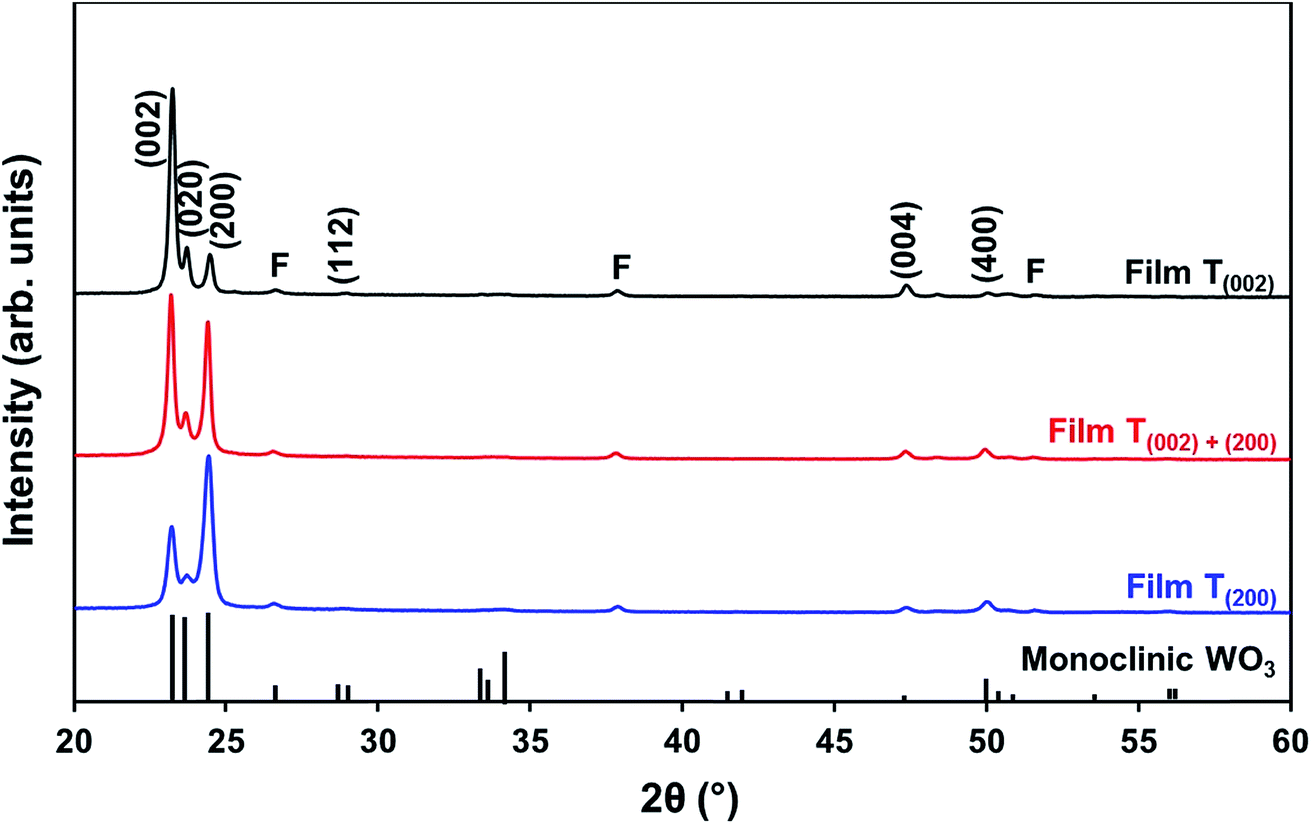 | ||
| Fig. 5 XRD spectra of films T(002), T(002)+(200), and T(200); reference data for monoclinic WO3 also are shown;11 F denotes peaks for FTO substrate. | ||
Pole figures for the (002), (020), and (200) planes were obtained in order to investigate the texture, i.e., the preferred orientation distribution, of the crystallised WO3 grains on the surface of the films (see Fig. S3†). These distributions are found to be symmetrical and those concentrated at the centre of the pole show only small azimuthal deviations (<10°) from the centre of the pole, indicating a minimal tilt of these planes from the substrate plane.
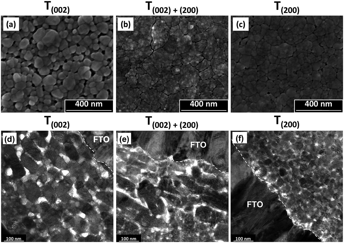 | ||
| Fig. 6 SEM secondary electron images of the surface morphologies (a–c) and corresponding TEM cross sectional images (d–f) of films T(002), T(002)+(200), and T(200). | ||
Film T(002). The low nucleation distribution density of the film deposited from PTA consisting of the lower tungsten concentration (0.05 mol L−1) and annealed at 500 °C for 2 h causes the formation of a porous nanostructure of isolated grains upon annealing. These features are a reflection of the low nuclei distribution density, which encourages the growth of isolated grains, where those nuclei in mutual contact coalesce into isolated agglomerates. These agglomerates grow into well formed grains with smooth surfaces and minimal indication of subgrain boundaries owing to the high annealing temperature of 500 °C.
Film T(002)+(200). The deposition from PTA containing high tungsten concentration (0.20 mol L−1) and annealing at 350 °C for 8 h results in the formation of a denser nanostructure consisting of large agglomerates of small subgrains. These features are a reflection of the high nucleation density, which facilitates retention of small grains prior to impingement with others and consequent densification within the agglomerates. The delaminated agglomerates may be due to the mixture of predominantly (002) and (200) orientations, which restricts coalescence and the preferred growth of one plane over the other. The agglomerate surfaces are rough because the low annealing temperature of 350 °C is insufficient to facilitate mass transfer and subgrain growth such that smooth and faceted grains would form.
Film T(200). The deposition from PTA containing high tungsten concentration (0.20 mol L−1) and annealing at 500 °C for 0.5 h results in features that reflect a compromise between annealing temperature (high) and annealing time (short): smaller agglomerates, larger subgrains (as indicated by the reduced charging from particles of greater diameter and hence less roughness), and less agglomerate shrinkage and delamination compared to film T(002)+(200). That is, the potential for the thermodynamically stable (200) plane to moderate the growth of large and well formed grains is limited by the short annealing time.
In the TEM cross sectional images of the preceding films, film T(002) demonstrates that the annealing conditions of high temperature (500 °C) and relatively short time (2 h) generate a nanostructure with a high proportion of discrete tabular WO3 grains oriented parallel to the substrate, although unaligned grains also are present. This tabular morphology has been observed before.36,37 In contrast, film T(200) exhibits nanostructures that essentially are equiaxed. In this case, the dominance of time is emphasised since these grains had insufficient time (0.5 h) to grow even though the highest temperature (500 °C) was used and generated the thermodynamically stable orientation. In the case of film T(002)+(200), a high proportion of tabular forms can be seen but their outlines are not distinct and the mottled appearance confirms the agglomerated nature of these grains observed in Fig. 6(b). The XRD data in Fig. 5, which show mixed (002) and (200) orientations, supports the conclusion of the presence of biaxially oriented subgrains within these tabular forms. The apparent contradiction that biaxially oriented subgrains within the agglomerates comprise uniaxially oriented tabular forms is resolved by the fact that the tabular shape derives from the agglomerates that form parallel to the substrate.
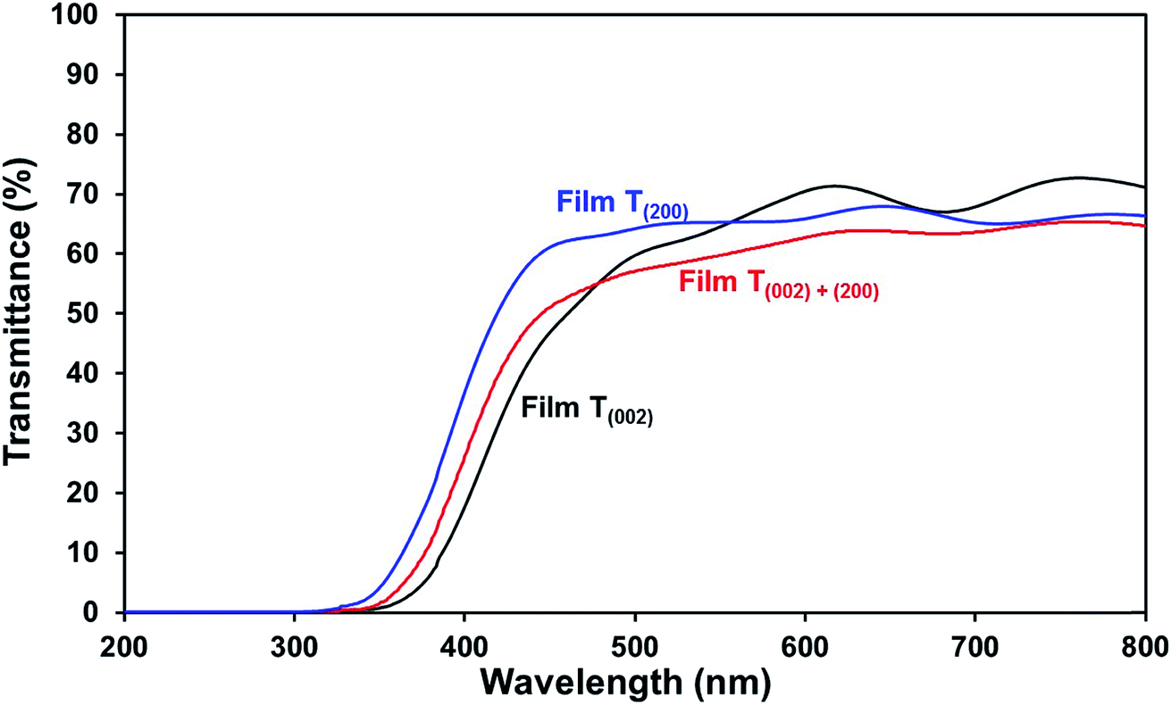 | ||
| Fig. 7 Optical transmittance spectra of films T(002), T(002)+(200), and T(200). | ||
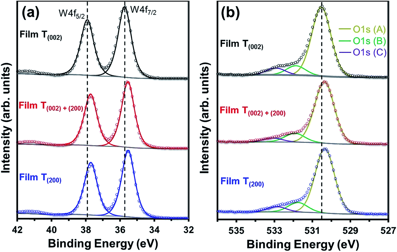 | ||
| Fig. 8 XPS spectra of (a) W4f and (b) O1s regions for films T(002), T(002)+(200), and T(200). | ||
The O1s (A) peak for film T(002) at 530.54 eV corroborates that the tungsten oxide composition is principally stoichiometric.45 Similar to the W4f peaks, all three O1s peaks in films T(002)+(200) and T(200) also shift to lower binding energies and this is attributed to their hypostoichiometry. Since the concentration of oxygen in the W–O lattice is invariant to the surface electronic properties, the area under the O1s (B) peak is normalised to that of the O1s (A) peak in order to obtain the relative concentrations of oxygen vacancies. As shown in Table 1, the normalised areas under the O1s (B) peaks follow the order T(200) > T(002)+(200) > T(002). This suggests that oxygen vacancies are formed more readily on the (200) plane than on the (002) plane.
Parenthetically, it can be noted that the peak current densities of the cyclic voltammograms of the films at approximately −0.2 V, shown in Fig. S4,† which correspond to the amount of H+ intercalated in the films due to electrochromism,50 are in the order T(200) > T(002)+(200) > T(002). These data are consistent with those reported by others,51,52 where lower current densities from cyclic voltammograms were obtained in electrochromic WO3 samples with lower oxygen vacancy concentrations. Vuong et al.52 related these observations to a decrease in the number of H+-capture sites.
The crystallographic effect on the formation of oxygen vacancies in the present work may be due to the structural anisotropy (W–O bond lengths) associated with the monoclinic cell of WO3, consistent with the crystallographic orientation-dependent oxygen vacancy formation energy obtained using density-functional theory (DFT) calculations.53 In addition, there also may be a nanostructural effect. That is, oxygen vacancies may form preferentially on the subgrain and grain boundary areas of the agglomerates of films T(002)+(200) and T(200) since these are well known as regions of highly defective structure that readily adsorb OH− groups to oxide surfaces.54 This nanostructural effect cannot be differentiated between these two films owing to the difficulty in precisely distinguishing the subgrain boundaries within the agglomerates.
It has been shown by Chatten et al.,55 using DFT calculations, that the oxygen vacancies associated with hypostoichiometric monoclinic WO3−x decreases the band gap owing to the decreased W–O bonding–antibonding interaction. This also has been shown in the work on WO3 films deposited on (100) single-crystal Si substrates by Diaz-Reyes et al.,56 who observed a direct correlation between the oxygen vacancy concentration and the optical indirect band gap. However, neither of these studies considered the potential effect of preferred orientation. Inspection of the X-ray diffraction data of Diaz-Reyes et al.56 shows that their films exhibited {002} preferred orientations and so this parameter may have had an unrecognised influence on the data.
It is well known that oxygen vacancies in randomly oriented transition metal oxides are responsible for the reduced band gaps compared to those of stoichiometric oxides.57–59 In contrast, the DFT calculations of the oxygen vacancy formation in W–O chains of monoclinic WO3 along different crystallographic directions, reported by Wang et al.,60 indicated that the crystallographic locations of the oxygen vacancies alter the electronic band structure. Similar to the theoretical-experimental validation described in the preceding paragraph, the present work also provides experimental validation for the theoretical calculations, both of which indicate that the twofold correlation between the oxygen vacancy concentration and the band gap is more correctly a threefold correlation that also includes the crystallographic locations of the oxygen vacancies.
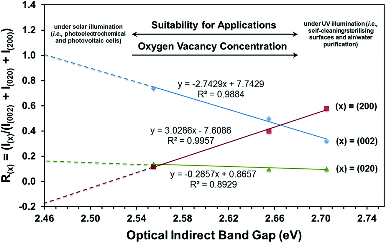 | ||
| Fig. 9 Threefold correlation between crystallographic orientation, oxygen vacancy concentration, and optical indirect band gap. | ||
(i) The (002) preferred orientation is critical to obtaining a minimal band gap.
(ii) Enhancement of the (002) preferred orientation is achieved by suppressing the (200) preferred orientation.
(iii) The (020) preferred orientation plays little role in alteration of the band gap.
(iv) Extrapolation of the R(002) plot to R(002) = 1.0 and hence a fully (002)-oriented film suggests that the minimal band gap that can be achieved is ∼2.46 eV.
(v) Since the R(200) and R(020) plots do not extrapolate to zero, the extrapolation of the R(002) plot can be considered only indicative.
It can be seen that the data in Fig. 9 can be used potentially as a diagnostic tool to engineer the electronic band structure of monoclinic WO3 thin films by control of their crystallographic orientation. These data also illustrate the decoupled effects of crystallographic orientation on the band gap and, by extension, the oxygen vacancy concentration of WO3 thin films.
It should be noted that, in addition to the two concurrent factors that affect the band gap, as examined above, there also are other controllable and uncontrollable factors that must be considered. These factors include the nanostructures (film thickness, grain size, roughness, porosity),19,61 mineralogies (polymorph, degree of crystallinity),62,63 chemical composition (stoichiometry, dopants, impurities),64,65 and structural defects (type and concentration).49,66 The films were prepared such that they possess the same thickness, surface roughness (see Fig. S5† for AFM analysis), degree of crystallinity, and elemental composition and so the effects from these factors have been minimised. That is, the present work has attempted to normalise all of the controllable variables, while the uncontrollable variables are those that are generated intrinsically in the films.
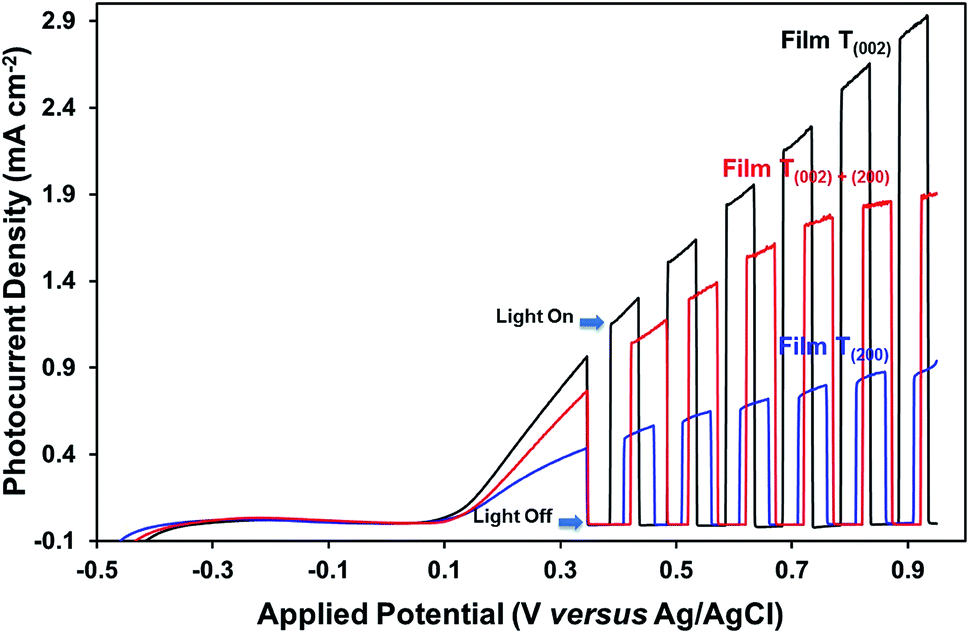 | ||
| Fig. 10 Linear potentiodynamic photocurrent densities of films T(002), T(002)+(200), and T(200). | ||
Optical band gap. The low band gap of film T(002) is beneficial to optical absorption, which enhances the photogeneration of charge carriers. This is supported by the decreased differences between the photocurrent densities of film T(002) and those of films T(002)+(200) and T(200) after normalisation to the total optical absorbance of the films, as illustrated in Fig. S7.† The differences in the absorbance-normalised photocurrent density of the films are due to factors (ii) and (iii) as follows:
Valence band maximum. The low valence band maximum of film T(002) results in the strong oxidising power of the photogenerated holes, which facilitates the oxidation of water molecules.
Oxygen vacancies. The oxygen vacancies may have different effects on the photoelectrochemical performance, depending on their locations in the photoelectrode. Only the oxygen vacancies present in one or two monolayers below the surface of the photoelectrode have beneficial effects because they act as reaction sites to facilitate the adsorption of reactants (viz., water molecules).49,67,68 However, if present in the top monolayer of the surface of the photoelectrode, the oxygen vacancies are likely to be saturated with adsorbed hydroxyl ions and thus are not available as reaction sites.69 If present in the bulk of the photoelectrode, the oxygen vacancies may act as recombination sites to trap photogenerated charge carriers.49,68
The photocurrent measurements (Fig. 10) show that the oxygen vacancies associated with the crystallographic orientations and nanostructures have a negative effect on the photoelectrochemical properties of the films. Assuming that the oxygen vacancies are distributed homogeneously on the surface and in the bulk of the films, the oxygen vacancies present in high concentration in the bulk of film T(200), relative to those of films T(002) and T(020)+(200), may have trapped and thereby enhanced the recombination of charge carriers during their transport to the back-contact of the films. The influence of preferred orientation in WO3 thin-film photoelectrodes on the photoelectrochemical properties also has been reported by others,15,29 where superior performance was observed for a (002)-dominant monoclinic WO3 film compared to its (200)-dominant counterpart due to its enhanced charge–transport properties.
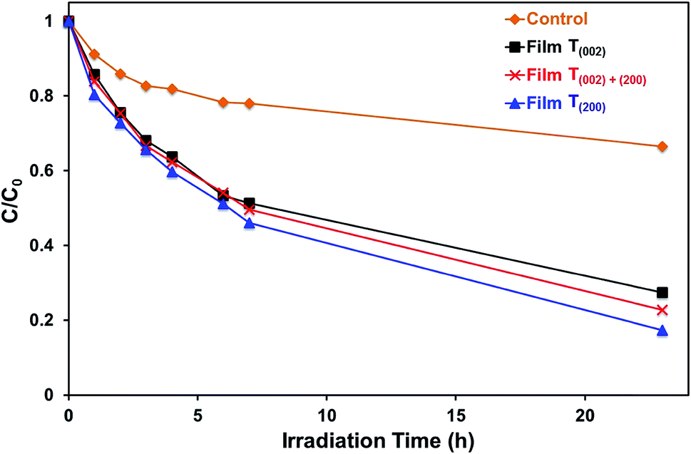 | ||
| Fig. 11 Photocatalytic degradation of methylene blue as a function of irradiation time t; C and C0 are the concentrations of methylene blue at irradiation time t and t = 0, respectively; major spectral output: 254 nm; C0 = 1 ppm. | ||
The data in Fig. 10, 11, and S8† suggest the different applications for which the data in Fig. 9 can be used. That is, for applications typically requiring UV irradiation, such as self-cleaning and self-sterilising surfaces and air and water purification, a high oxygen vacancy concentration is advantageous, so (200) preferred orientation is beneficial. Alternatively, for applications requiring photosensitivity in the visible light region, such as solar energy applications, (002) preferred orientation is desirable.
4. Conclusions
Monoclinic tungsten oxide films with tunable preferred (002) and (200) orientations parallel to FTO substrates were electrodeposited from PTA solutions, followed by post-deposition annealing. The crystallographic predominance of the films was controlled by varying the nucleation density and the thermally-induced recrystallisation kinetics, where the former and the latter were manipulated by changing the tungsten concentrations of the PTA solutions and the annealing conditions, respectively. The importance of the nanostructures of the films was emphasised in that both the annealing temperature and time that generated specific crystallographic predominance depended significantly on the tungsten concentration of the PTA solution, which determined the distribution density of the tungsten oxide nuclei and the proximity of the resultant grains. These grains underwent growth of the thermodynamically stable (200) plane such that, under the conditions of maximal temperature and/or time, a preferred (200) orientation parallel to the substrate resulted. Hence, the tungsten concentration of the PTA solution and the annealing temperature and time can be controlled to yield nanostructures of specific proportions of preferred crystallographic orientations in electrodeposited WO3 thin films.The present work shows that the highest photocurrent density measured under the illumination of simulated solar light was obtained in the film with (002) preferred orientation, which exhibits a relatively low optical band gap, low valence band maximum, and low oxygen vacancy concentration. These conditions favour the photogeneration of charge carriers with photogenerated holes of strong oxidising power and the suppression of charge carrier recombination owing to minimal bulk oxygen vacancy concentration, which traps charge carriers. In contrast, the highest efficiency in the photodegradation of methylene blue under UV illumination (254 nm and 365 nm) is obtained in the film with (200) preferred orientation, which shows the highest concentration of oxygen vacancies, where those located in the first one or two monolayers of the surface contribute as the surface reaction sites.
Control of the crystallographic orientations of WO3 thin films without the use of expensive substrates for epitaxial growth or growth-directing agents (which are more viably applicable to powder synthesis, not films) provides a feasible technique to tune the nanostructure for specific performance parameters. Further, the data for the correlation between the crystallographic orientation, oxygen vacancy concentration, and optical indirect band gap can be used as a diagnostic tool that is applicable to the fabrication of films suitable for uses requiring photosensitivities in different regions of the solar spectrum.
Conflicts of interest
There are no conflicts to declare.Acknowledgements
This work was supported in part by a project funded by the Australian Research Council (ARC, 110105264). The authors are grateful for the characterisation facilities from Mark Wainwright Analytical Centre at UNSW Sydney. W. L. Kwong gratefully acknowledges the receipt of a UNSW International Postgraduate Award.References
- M. Wang, Y. Zhang, Y. Zhou, F. Yang, E. J. Kim, S. H. Hahn and S. G. Seong, CrystEngComm, 2013, 15, 754–763 RSC.
- H. G. Yang, G. Liu, S. Z. Qiao, C. H. Sun, Y. G. Jin, S. C. Smith, J. Zou, H. M. Cheng and G. Q. Lu, J. Am. Chem. Soc., 2009, 131, 4078–4083 CrossRef PubMed.
- Z. Lai, F. Peng, Y. Wang, H. Wang, H. Yu, P. Liu and H. Zhao, J. Mater. Chem., 2012, 22, 23906–23912 RSC.
- T. Bak, J. Nowotny, M. Rekas and C. C. Sorrell, Int. J. Hydrogen Energy, 2002, 27, 991–1022 CrossRef.
- E. L. Miller, On Solar Hydrogen and Nanotechnology, John Wiley and Sons, Singapore, 2009 Search PubMed.
- C. A. Grimes, O. K. Varghese and S. Ranjan, Light, Water, Hydrogen: The Solar Generation of Hydrogen by Water Photoelectrolysis, Springer Science+Business Media, New York, 2008 Search PubMed.
- Y. P. Xie, G. Liu, L. Yin and H.-M. Cheng, J. Mater. Chem., 2012, 22, 6746–6751 RSC.
- M. A. Butler and D. S. Ginley, J. Electrochem. Soc., 1978, 125, 228–232 CrossRef.
- Y. Xu and M. A. A. Schoonen, Am. Mineral., 2000, 85, 543–556 CrossRef.
- E. Lassner and W. D. Schubert, in Tungsten: Properties, chemistry, technology of the element, alloys, and chemical compoundsKluwer Academic/Plenum Publishers, New York, 1999, pp. 133–178 Search PubMed.
- P. M. Woodward, A. W. Sleight and T. Vogt, J. Phys. Chem. Solids, 1995, 56, 1305–1315 CrossRef.
- G. Hodes, D. Cahen and J. Manassen, Nature, 1976, 260, 312–313 CrossRef.
- X. Han, X. Han, L. Lia and C. Wang, New J. Chem., 2012, 36, 2205–2208 RSC.
- D. Zhang, S. Wang, J. Zhu, H. Li and Y. Lu, Appl. Catal., B, 2012, 123–124, 398–404 CrossRef.
- J. Zhang, P. Zhang, T. Wang and J. Gong, Nano Energy, 2015, 11, 189–195 CrossRef.
- J. Y. Zheng, Z. Haider, T. K. Van, A. U. Pawar, M. J. Kang, C. W. Kim and Y. S. Kang, CrystEngComm, 2015, 17, 6070–6093 RSC.
- J. Y. Zheng, G. Song, C. W. Kim and Y. S. Kang, Nanoscale, 2013, 5, 5279–5282 RSC.
- S. Hilaire, M. J. Süess, N. Kränzlin, K. Bieńkowski, R. Solarska, J. Augustyński and M. Niederberger, J. Mater. Chem. A, 2014, 2, 20530–20537 RSC.
- W. L. Kwong, N. Savvides and C. C. Sorrell, Electrochim. Acta, 2012, 75, 371–380 CrossRef.
- P. Bermejo and J. A. Cocho de Juan, in Lead: Chemistry, analytical aspects, environmental impact and health effects, ed. J. S. Casas and J. Sordo, Elsevier Amsterdam, 2006, ch. 5, p. 232 Search PubMed.
- D. Sarkar and A. Haldar, Physical And Chemical Methods In Soil Analysis: Fundamental concepts of analytical chemistry and instrumental techniques, New Age International, New Delhi, 2005 Search PubMed.
- M. Deepa, A. K. Srivastava, T. K. Saxena and S. A. Agnihotry, Appl. Surf. Sci., 2005, 252, 1568–1580 CrossRef.
- M. Deepa, M. Kar and S. A. Agnihotry, Thin Solid Films, 2004, 468, 32–42 CrossRef.
- G. W. Grodstein, X-Ray Attenuation Coefficients From 10 kev to 100 kev, NBS Circular 583, National Bureau of Standards, Washington, D.C., 1957, pp. 1–54 Search PubMed.
- S. Tanisaki, J. Phys. Soc. Jpn., 1960, 15, 573–581 CrossRef.
- M. N. Huda, Y. Yan, C. Y. Moon, S. H. Wei and M. M. Al-Jassim, Phys. Rev. B: Condens. Matter Mater. Phys., 2008, 77, 195102 CrossRef.
- A. Nakaruk, G. Kavei and C. C. Sorrell, Mater. Lett., 2010, 64, 1365–1368 CrossRef.
- Z. Guo and L. Tan, Fundamentals and Applications of Nanomaterials, Artech House, Norwood, MA, 2009 Search PubMed.
- J. Y. Zheng, G. Song, J. Hong, T. K. Van, A. U. Pawar, D. Y. Kim, C. W. Kim, Z. Haider and Y. S. Kang, Cryst. Growth Des., 2014, 14, 6057–6066 CrossRef.
- K. Tomioka and T. Fukui, in Semiconductor nanostructures for optoelectronic devices: Processing, characterization, and applications, ed. G. C. Yi, Springer-Verlag, Berlin Heidelberg, 2012, p. 67–102 Search PubMed.
- H. Fredriksson and U. Akerlind, Solidification and crystallization processing in metals and alloys, John Wiley & Sons, United Kingdom, 2012 Search PubMed.
- S. A. Manafi, M. R. Rahimipour and A. Soltanmoradi, Int. J. Phys. Sci., 2012, 7, 5772–5778 Search PubMed.
- S. Park, J. O. Baker, M. E. Himmel, P. A. Parilla and D. K. Johnson, Biotechnol. Biofuels, 2010, 3, 10 CrossRef PubMed.
- K. S. Kim, C. M. Ryu, C. S. Park, G. S. Sur and C. E. Park, Polymer, 2003, 44, 6287–6295 CrossRef.
- A. Kumar and D. Saikia, in Specialty Polymers: Materials and Applications, ed. F. Mohammad, I. K. International Publishing House, New Delhi, 2007, ch. 13, p. 464 Search PubMed.
- D. L. Chen, X. X. Hou, T. Li, L. Yin, B. B. Fan, H. L. Wang, X. J. Li, H. L. Xu, H. X. Lu, R. Zhang and J. Sun, Sens. Actuators, B, 2011, 153, 373–381 CrossRef.
- L. N. Geng, Synth. Met., 2010, 160, 1708–1711 CrossRef.
- J. Tauc, Mater. Res. Bull., 1968, 3, 37–46 CrossRef.
- G. Liu, C. Sun, H. G. Yang, S. C. Smith, L. Wang, G. Q. Lu and H. M. Cheng, Chem. Commun., 2010, 46, 755–757 RSC.
- X. Wan, X. Zhao, H. L. W. Chan, C. L. Choy and H. Luo, Mater. Chem. Phys., 2005, 92, 123–127 CrossRef.
- G. Wang, Y. Ling, H. Wang, X. Yang, C. Wang, J. Z. Zhang and Y. Li, Energy Environ. Sci., 2012, 5, 6180–6187 RSC.
- L. Cheng, Y. Hou, B. Zhang, S. Yang, J. W. Guo, L. Wu and H. G. Yang, Chem. Commun., 2013, 49, 5945–5947 RSC.
- S. Ostachaviciute, J. Baltrusaitis and E. Valatka, J. Appl. Electrochem., 2010, 40, 1337–1347 CrossRef.
- M. Deepa, A. K. Srivastava, S. N. Sharma, Govind and S. M. Shivaprasad, Appl. Surf. Sci., 2008, 254, 2342–2352 CrossRef.
- J. F. Moulder, W. F. Stickle, P. E. Sobol and K. D. Bomben, Handbook of X-ray Photoelectron Spectroscopy, Perkin-Elmer Corporation, Minnesota, USA, 1992 Search PubMed.
- J. Li, Y. Liu, Z. Zhu, G. Zhang, T. Zou, Z. Zou, S. Zhang, D. Zeng and C. Xie, Sci. Rep., 2013, 3, 2409 CrossRef PubMed.
- S. Rahimnejad, J. H. He, W. Chen, K. Wu and G. Q. Xu, RSC Adv., 2014, 4, 62423–62429 RSC.
- J. Wang, Z. Wang, B. Huang, Y. Ma, Y. Liu, X. Qin, X. Zhang and Y. Dai, ACS Appl. Mater. Interfaces, 2012, 4, 4024–4030 CrossRef PubMed.
- J. Gan, X. Lu, J. Wu, S. Xie, T. Zhai, M. Yu, Z. Zhang, Y. Mao, S. C. I. Wang, Y. Shen and Y. Tong, Sci. Rep., 2013, 3, 1021 CrossRef PubMed.
- L. L. Yang, D. T. Ge, J. P. Zhao, Y. B. Ding, X. P. Kong and Y. Li, Sol. Energy Mater. Sol. Cells, 2012, 100, 251–257 CrossRef.
- C. C. Liao, F. R. Chen and J. J. Kai, Sol. Energy Mater. Sol. Cells, 2007, 91, 1258–1266 CrossRef.
- N. M. Vuong, D. Kim and H. Kim, J. Mater. Chem. C, 2013, 1, 3399–3407 RSC.
- M. Gerosa, C. Di Valentin, G. Onida, C. E. Bottani and G. Pacchioni, J. Phys. Chem. C, 2016, 120, 11716–11726 CrossRef.
- J. Q. Yan, G. J. Wu, N. J. Guan, L. D. Li, Z. X. Li and X. Z. Cao, Phys. Chem. Chem. Phys., 2013, 15, 10978–10988 RSC.
- R. Chatten, A. V. Chadwick, A. Rougier and P. J. D. Lindan, J. Phys. Chem. B, 2005, 109, 3146–3156 CrossRef PubMed.
- J. Diaz-Reyes, R. Castillo-Ojeda, M. Galvan-Arellano and O. Zaca-Moran, Adv. Condens. Matter Phys., 2013, 2013, 591787 Search PubMed.
- Q. Kang, J. Cao, Y. Zhang, L. Liu, H. Xu and J. Ye, J. Mater. Chem. A, 2013, 1, 5766–5774 RSC.
- S. A. Ansari, M. M. Khan, S. Kalathil, A. Nisar, J. Lee and M. H. Cho, Nanoscale, 2013, 5, 9238–9246 RSC.
- Y. Lv, Y. Liu, Y. Zhu and Y. Zhu, J. Mater. Chem. A, 2014, 2, 1174–1182 RSC.
- F. Wang, C. Di Valentin and G. Pacchioni, Phys. Rev. B: Condens. Matter Mater. Phys., 2011, 84, 073103 CrossRef.
- W. L. Kwong, A. Nakaruk, P. Koshy and C. C. Sorrell, J. Phys. Chem. C, 2013, 117, 17766–17776 CrossRef.
- F. Di Quarto, G. Russo, C. Sunseri and A. Di Paola, J. Chem. Soc., Faraday Trans. 1, 1982, 78, 13 RSC.
- A. Nakaruk, D. Ragazzon and C. C. Sorrell, Thin Solid Films, 2010, 518, 3735–3742 CrossRef.
- Y. C. Nah, I. Paramasivam, R. Hahn, N. K. Shrestha and P. Schmuki, Nanotechnology, 2010, 21, 105704 CrossRef PubMed.
- D. Paluselli, B. Marsen, E. L. Miller and R. E. Rocheleau, Electrochem. Solid-State Lett., 2005, 8, G301–G303 CrossRef.
- B. Cole, B. Marsen, E. Miller, Y. F. Yan, B. To, K. Jones and M. Al-Jassim, J. Phys. Chem. C, 2008, 112, 5213–5220 CrossRef.
- M. Ahsan, M. Z. Ahmad, T. Tesfamichael, J. Bell, W. Wlodarski and N. Motta, Sens. Actuators, B, 2012, 173, 789–796 CrossRef.
- X. Pan, M. Q. Yang, X. Fu, N. Zhang and Y. J. Xu, Nanoscale, 2013, 5, 3601–3614 RSC.
- R. Mehmood, X. Wang, P. Koshy, J. L. Yang and C. C. Sorrell, CrystEngComm, 2018, 20, 1536–1545 RSC.
- W. Y. Wang and B. R. Chen, Int. J. Photoenergy, 2013, 2013, 348171 Search PubMed.
Footnote |
| † Electronic supplementary information (ESI) available. See DOI: 10.1039/c8se00239h |
| This journal is © The Royal Society of Chemistry 2018 |