
 Open Access Article
 This Open Access Article is licensed under a Creative Commons Attribution-Non Commercial 3.0 Unported Licence
Highly sensitive metal-grid strain sensors via water-based solution processing†
Seungwoo Oh,
Jin Kim and
Suk Tai Chang *
*
School of Chemical Engineering and Materials Science, Chung-Ang University, 84 Heukseok-ro, Dongjak-gu, Seoul 06974, Republic of Korea. E-mail: stchang@cau.ac.kr
First published on 18th December 2018
Abstract
Strain sensor technologies have been spotlighted for their versatility for healthcare, soft robot, and human–robot applications. Expecting large future demands for such technology, extensive studies have investigated flexible and stretchable strain sensors based on various nanomaterials and metal films. However, it is still challenging to simultaneously satisfy parameters such as sensitivity, stretchability, linearity, hysteresis, and mass producibility. In this work, we demonstrate a novel approach for producing highly sensitive metal-grid strain sensors based on an all-solution process, which is suitable for mass production. We investigated the effects of the width of the metal grid and width/spacing ratio on the piezoresistivity of the strain sensors. The metal grid strain sensors exhibited high sensitivity (gauge factor of 4685.9 at 5% strain), rapid response time (∼18.6 ms), and superior strain range (≤5%) compared to other metal-based sensors. We demonstrated that the sensors could successfully convert voice signals and tiny movements of fingers and muscles into electrical signals. In addition, the metal-grid strain sensors were produced using a low-cost procedure without toxic solvent via an all water-based solution process, which is expected to allow the integration of such metal-grid strain sensors into future highly sensitive physical sensing devices.
Introduction
Wearable devices with flexibility or stretchability have attracted tremendous attention as emerging next-generation portable electronics due to their versatility, and compatibility with other electronic devices.1–4 Recently, some wearable devices have been commercialized, e.g., smart watches and eyeglasses, and wearable bands with additional functions for health monitoring or detection of human body motion by various sensors within the devices.2,5–7 Such sensor systems, especially for detecting body movements, need to be flexible, stretchable, and skin-mountable, while having high sensitivity. However, conventional metal- or semiconductor-based sensors are not flexible or stretchable (typical tensile strain, ε ≤ 1–2%).8–10 Therefore, alternative conducting materials and fabrication techniques are required to overcome the limitations of conventional rigid sensors; hence, the resulting sensor system can be used for a wide range of potential applications, such as human–machine interfaces, soft robots, and various wearable electronics.11–15Alternative materials for such sensors include carbon-based nanomaterials, such as graphene,16–20 carbon black,21–24 carbon nanotubes (CNT),25–27 and others,28,29 which have been widely applied for fabrication of strain sensors to measure various human body motions. Carbon-based strain sensor systems have been realized using filtration,18,30 multiple dip-coating,17 or paint brush.22 A promising strain sensor uses fragmented CNT papers on polydimethylsiloxane (PDMS).30 CNT papers with various thicknesses were fabricated by filtration using a ceramic filtration membrane. Amjadi et al. prepared graphite films by bar coating on Eco-flex substrate which showed surface cracks after oxygen plasma treatment for various time periods.29
In other studies, elastomeric polymer microchannels filled with ionic liquids or liquid metals were recently exploited as piezo-capacitive or piezo-resistive strain sensors.31–33 However, these liquid-type strain sensors could have some of drawbacks, including leakage under repeated deformation of the channel, harmful effects of the leaked liquids on human skin, or relatively low gauge factors (GF) compared to strain sensors with solid conductive nanomaterials.
Metal nanoparticles are prospective materials as they are easy to synthesize, simple to fabricate using solution-based methods, and the diameter of nanoparticles can be controlled.2,34–36 An accurate mechano-electronic system was demonstrated using a monolayer strip of gold nanoparticles (Au NP) with diameters of 50 nm deposited on polyethylene terephthalate (PET).37 The Au NP strip (width of 1–1.5 μm) was formed using a modified convective assembly method. A different NP-based strain sensor used Pd micro-stripes patterned on polyimide substrate by PDMS stamping, followed by thermal treatment to form the nanocrystals.38 Although numerous studies have been reported, the majority of the devices showed low sensitivity; in the previously discussed studies, low GF values of 70 (for the Au NP strip) and ∼390 (for semi-transparent Pd stripes) were reported.
Some studies using nanomaterials exploit tunneling effects where electrons can pass through very thin (<1–2 nm) nonconductive barriers between conductive materials.39,40 Stretching the sensor reduces the tunneling effect by widening the barriers through which the electrons need to pass, which increases the electrical resistance. The studies mentioned above have shown such low sensitivity that another approach using crack propagation is attracting attention. In thin metal foils or plasma-treated polymer substrates, cracks begin to appear in weakened areas that propagate in the transversal direction as stress is applied to the metal film.22,29,41–43 Cracks degrade conduction paths, greatly increasing the electrical resistance. In order to design highly sensitive sensors, crack propagation is an outstanding mechanism. A cracked Pt metal film on a polyurethane acrylate (PUA) substrate has been proposed, which shows linear behavior, low hysteresis, repeatability, and also high deformation sensitivity (GF = 2000).42 Kim et al. enhanced this design to produce a more sensitive sensor (GF = 16![[thin space (1/6-em)]](https://www.rsc.org/images/entities/char_2009.gif) 000) and demonstrated superior signal-to-noise (SNR ∼ 35) by increasing the depth of the cracks.44 Similarly, cracked Au films on polydimethylsiloxane (PDMS) elastomers exhibited outstanding sensitivity (GF = 5000).43 Despite exceptional piezoresistive behavior, the cracked metal films had extremely low stretchability, ε = ∼2% and 1% for the cracked Pt and Au films, respectively. Additionally, these metal films were formed using relatively expensive processes under high-vacuum conditions.41,42,45 Although metal thin films are promising candidates for future high-sensitivity strain sensors, further investigation of the stretchability, linearity, fabrication process, and hysteresis behavior is required.
000) and demonstrated superior signal-to-noise (SNR ∼ 35) by increasing the depth of the cracks.44 Similarly, cracked Au films on polydimethylsiloxane (PDMS) elastomers exhibited outstanding sensitivity (GF = 5000).43 Despite exceptional piezoresistive behavior, the cracked metal films had extremely low stretchability, ε = ∼2% and 1% for the cracked Pt and Au films, respectively. Additionally, these metal films were formed using relatively expensive processes under high-vacuum conditions.41,42,45 Although metal thin films are promising candidates for future high-sensitivity strain sensors, further investigation of the stretchability, linearity, fabrication process, and hysteresis behavior is required.
Herein, we propose a novel approach to fabricate high-sensitivity metal-grid strain sensors using a water-based solution process. In this process, AuNPs were deposited on a (3-aminopropyl)triethoxysilane (APTES) monolayer which was patterned with varied grid sizes and transferred to polydimethylsiloxane (PDMS) to form the desired grid patterns. Silver ions were reduced with AuNPs to form grid-patterned Au–Ag conductors on the PDMS. To characterize these strain sensors with diverse grid sizes, thorough examination of their behavior under cyclic motion, durability tests, step tests, and bending tests in the concave/convex directions were performed. In order to evaluate the sensors for potential healthcare and human–machine interface applications, the metal-grid strain sensors were used to detect voice signal and very small motions of the body parts and muscles. Our sensors are expected to be applied in wearable devices and various flexible electronic devices in the future.
Results and discussion
A schematic diagram showing an overview of the fabrication procedure is shown in Fig. 1a. Glass slides were treated with a piranha solution to clean them and introduce hydroxyl groups. The hydrophilized glass was immersed in the APTES solution to be silanized. Glasses with the APTES coating were annealed to promote further reaction and sonicated to remove unreacted APTES residue. Various grid patterns were produced by etching APTES layers through masks, such as 5:5, 10:10, 20:20, 30:30, 50:50, 5:25, 20:100 (grid width:spacing; μm). AuNPs were selectively deposited on the grid-patterned APTES layer as the amine group, which is the terminal group of APTES, attaches to AuNPs via electrostatic interactions.46–48 PDMS pre-polymer was cast on the glass using spin coating and then cured. When peeled off the glass, the cured PDMS removes the AuNPs in the form of the desired grid pattern. AuNPs, which were embedded partly in the PDMS substrate, acted as seeds for reducing Ag ions and forming Au–Ag core–shell structures. A final annealing step melted the Au–Ag alloy to form a conductive layer. Further details of the fabrication process are described in the experimental section.
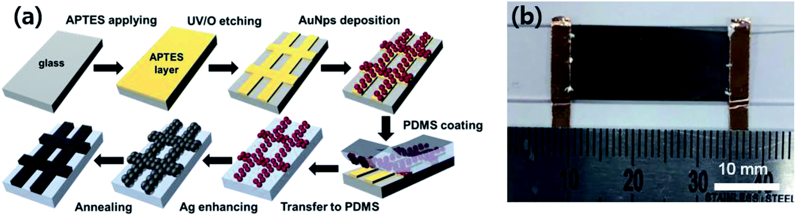 | ||
| Fig. 1 (a) Schematic illustration of fabrication process of metal grid structural strain sensor. (b) Photograph of strain sensor with 5:5 (width:spacing, μm) grid pattern. | ||
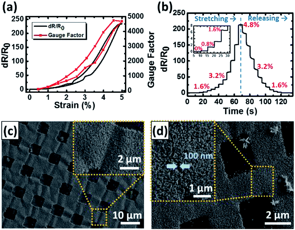
Using this method, 5 μm-wide metal grids with 5 μm or 25 μm spacings were the smallest dimensions that could be produced on the PDMS substrate, which is considered high-resolution patterning on an elastomer. A photograph of the strain sensor with a 5:5 metal grid is shown in Fig. 1b. Ag metal grids with different width/spacing ratios are shown in Fig. 2, while OM images of all specimens are shown in Fig. S1 and S2.† Wrinkles were formed during annealing due to the different thermal expansion coefficients of PDMS and Ag, as confirmed by FE-SEM images (Fig. 2).49
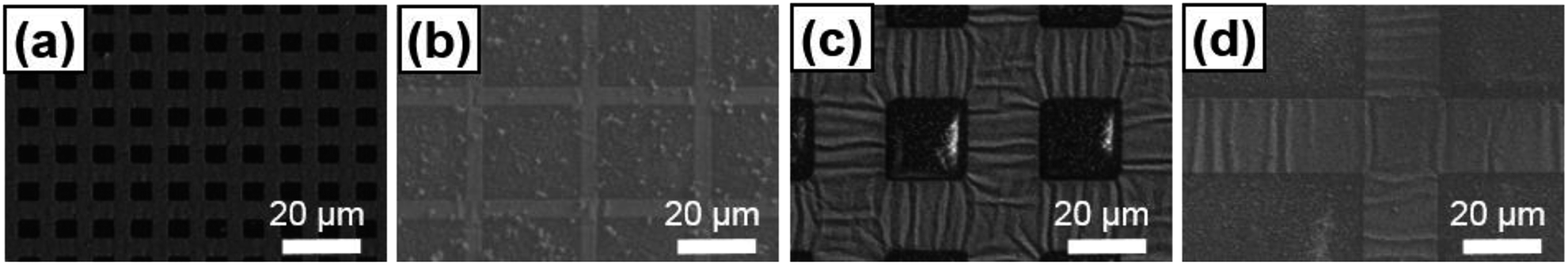 | ||
| Fig. 2 Electron microscopy images of strain sensors with different grid sizes and spacings (grid width:spacing, μm). (a) 5:5 (b) 5:25 (c) 20:20 (d) 20:100. | ||
The piezoresistive behavior of the strain sensors with various metal grid sizes was evaluated via cyclic loading/unloading tensile tests up to 1%, 3%, or 5% strain at a speed of 1.66 mm s−1 (Fig. S3–S5†). Strain sensors with 5:5, 10:10, 20:20, 30:30, and 50:50 metal grids (different widths, but the same width/spacing ratio), were used to demonstrate the effect of the metal grid width on the piezoelectric sensitivity (Fig. 3a). A complete film without any pattern showed the lowest relative change in resistance (lowest sensitivity), while the metal-grid sensors with smaller widths showed the higher sensitivity. The 5:5 grid strain sensor showed the highest sensitivity at 3% strain and 5% strain both (GF = 4685.9 at 5% strain).
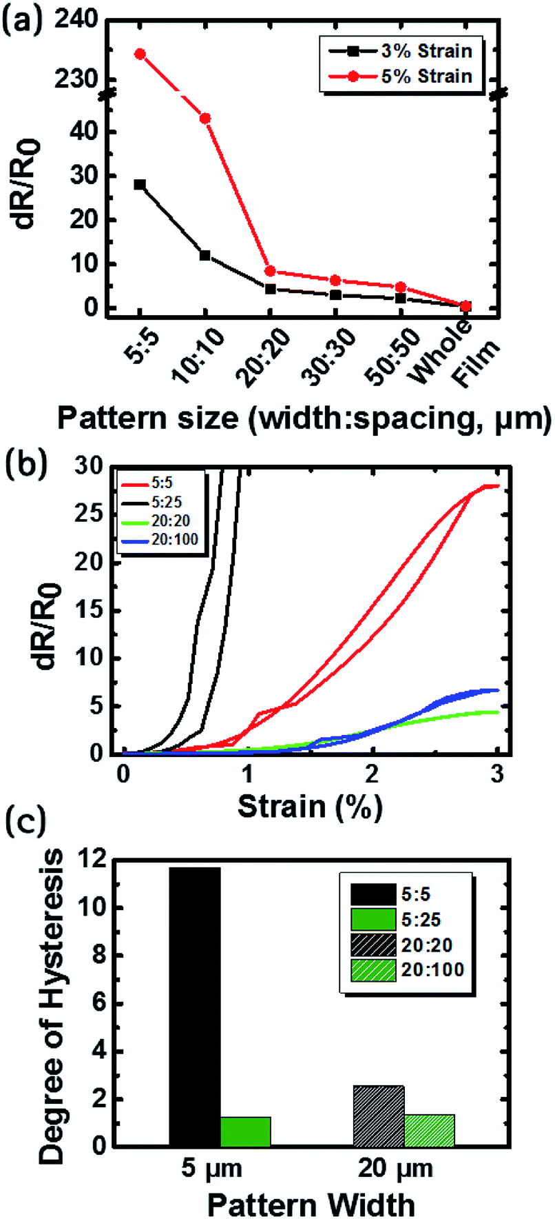 | ||
| Fig. 3 The effects of the grid width and spacing on the strain sensor behaviour. (a) The maximum relative change in resistance of various strain sensors with different pattern sizes but the same width/spacing ratio for 3% strain (black) and 5% strain (red). (b) Relative change in resistance as a function of strain with different grid sizes and width/spacing ratio, demonstrating the effect of width/spacing on sensitivity. (c) The influence of pattern size and width/spacing ratio on degree of hysteresis [DH = (AS − AR)/AS] under 3% cyclic strain. | ||
The correlation between width/spacing ratio of the pattern and the sensitivity of the sensor was also investigated (Fig. 3b). For the sensors with widths of 5 μm or 20 μm, lower width/spacing ratios resulted in more sensitive sensors. Although 5:25 grid sensor showed extremely high sensitivity (GF ∼ 20000 at 3% strain), it had poor stability under cyclic testing (Fig. S5d†). In addition, the pattern size influenced the degree of hysteresis [DH = (AS − AR)/AR], which is defined in a previous work50 (Fig. 3c). Metal grid strain sensors with smaller widths showed larger hysteresis. Smaller width/spacing ratios resulted in higher sensitivity and larger AR values, and consequently lower DH. Although the 5:5 grid strain sensor showed the highest DH among all specimens, it had competitive hysteresis (DH = 11.68). The uniform signals from cyclic motion of 5:5 grid strain sensors are shown in Fig. S4a.† The loading/unloading cycle (black) and the electrical signal converted to the GF (red) as functions of strain are shown in Fig. 4a. The 5:5 grid strain sensor showed the highest GF of 4685.9 at 5% strain. In the one-step test performed at 0.2% strain steps, the sensor showed a clear response and very short response time of 18.6 ms (Fig. S6†). The detectability test using a very small deformation (<0.2% strain) was not possible using the available equipment. Under 10% and 15% strain, the peak electrical signals decreased with increasing cycle number (Fig. S7†).
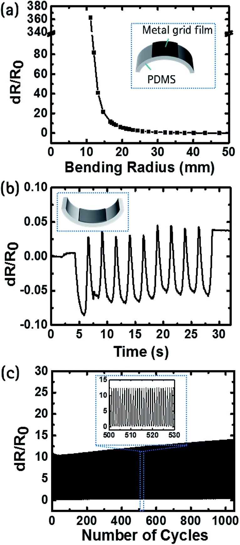 | ||
| Fig. 4 Performances of 5:5 strain sensors. Relative change in resistance as a function of time during (a) convex and (b) concave directional bending. Insets show the bending direction of the strain sensor with conducting (black) and PDMS (grey) substrates. (c) Durability test of sensor with strain up to ε = 0.6% at a speed of 1.67 mm s−1. The inset shows the signal over cycle numbers of 500–530. | ||
The stair-step tests showed distinct resistance signals in response to each step of 0.4% strain (Fig. 4b). A wrinkled structure was observed before applying strain (Fig. 4c) and cracks appeared as tensile strain was applied (Fig. 4d). The major piezoelectric sensing mechanism of the metal-grid strain sensor was crack propagation in the metal film. Some parts of the elongated metal film became thin and even cracked in the transversal direction to that of the applied strain (Fig. S8†). Although electrons pass through partially connected pathways near cracks in the conductor, grid conductor with smaller widths showed drastic deterioration of these conductive pathways. Hence, metal grids with narrower widths showed higher sensitivity. The cracks reducing the electrical conductive path appeared in the straight sections of the grid, rather than at the intersections (Fig. S8†). The grid patterns with lower width/spacing ratios had larger open spaces, which could explain the effect of the width/spacing ratio on the sensitivity.
The electrical responsivity to the bending radius as well as tensile strain is crucial performance of a strain sensor. Metal-grid strain sensors were tested under convex (Fig. 5a) and concave (Fig. 5b) bending motions. Convex bending resulted in a positive signal, i.e., an increase in the resistance due to tensile strain applied to the sensing region. Under tensile strain, the wavelength of the wrinkle increased and its amplitude decreased, resulting in an increase in resistance. The electrical response increased steeply at a comparatively low bending radius (15 mm) due to increased cracks in the metal film. On the contrary, concave bending resulted in negative resistance values. The compressive strain applied during concave bending increases the amplitude of the wrinkle and induced a concentrated metal film, resulting in a decrease in electrical resistance of the Ag conductor. In addition, the metal-grid strain sensors showed good durability for over 1000 loading/unloading cycles (Fig. 5c). Some flexible strain sensors recently reported is arranged in comparison table with important characteristics (Table S1†). This work shows outstanding sensitivity and large sensing range compared to metal-based strain sensors.
 | ||
| Fig. 5 Piezoresistive behaviour and FE-SEM images of 5:5 (grid width:spacing, μm) metal-grid strain sensors. (a) Relative change in resistance (black) and gauge factor (red) as a function of strain up to ε = 5%. (b) The stair-step test was performed up to 4.8% strain and each step was 0.4% strain. The inset shows the electrical signal under 2% strain. FE-SEM images of 5:5 patterned strain sensor (c) before and (d) after tensile strain test up to ε = 20%. The inset images are enlarged (c) wrinkle structure of conductor and (d) crack in the metal film. | ||
To verify the viability of the metal-grid strain sensors for practical applications, sensing of diverse motions of the body and voice signals was demonstrated. A sensor was mounted on the joint of an index finger and the finger was bent at two different angles (Fig. 6a). Due to the ultrahigh responsivity of the sensor, slight bending resulted in a clear electrical signal and the tiny angular movement was distinguished. The sensor was also applied to detect even smaller body movements; jerking of the triceps muscle was detected using the sensor (Fig. 6b). In addition, closing and opening a fist, and moving the antebrachial muscle between the wrist and elbow were detected. The sensor attached to the antebrachial muscle converted rapid motions to clear electrical signals (Fig. 6c).
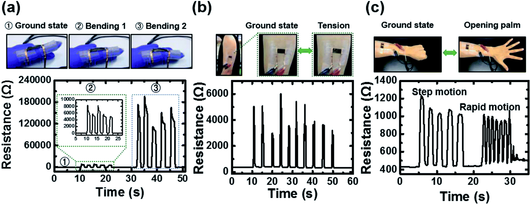 | ||
| Fig. 6 The electrical signals which is transformed from motion of body. (a) The sensor was attached on the joint of finger and the bending of finger was detected via strain senor. The angle of joint was two types and named as bending 1 (lower bending) and bending 2 (higher bending). (b) The target to sensing was stiffening of triceps and the resistance was expressed as a function of time. (c) The antebrachial muscle moves along to closing (ground state) and opening palms. This movement was converted to electrical signal through strain sensor. | ||
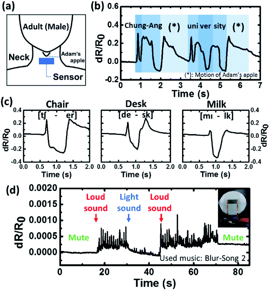
Considering other applications, a human voice signal from a volunteer or speaker was measured distinctively using these sensors. The strain sensor was placed on the neck under the Adam's apple of an adult male to sense vocal signals, as illustrated in Fig. 7a. The words “Chung-Ang University”, “Chair”, “Desk”, and “Milk” were spoken and the signals were analyzed by recording videos. The phrase “Chung-Ang University” was divided into five parts Chung/Ang/Uni/ver/sity. The motion of the neck and vocal cords, as well as the acoustic vibration stimulated the sensor. Jumps in the signal were from elongation from movement, and vibration, while drops in the signal were due to bending of the sensor in the concave direction (losing tension) (Fig. 7b). The words “Chair”, “Desk”, and “Milk” were distinguished by piezoresistive signals (Fig. 7c). The sensor was also placed on a speaker and used to produce signals from the sound waves. Light music composed of guitar and drums showed insignificant fluctuations in the resistance, while heavy sound accompanied by bass guitar, showed drastic variations in the signal.
 | ||
| Fig. 7 Applications for detecting voice and sound signals. (a) Illustration of sensor position to detect voice signals. The sensor was attached under the Adam's apple of the volunteer. (b) The vocal stimulus of words “Chung-Ang University” were expressed as an electrical signal via the strain sensor. (c) The words “chair”, “desk”, and “milk” were also distinguished by an electrical resistance signal. (d) The strain sensor was fixed on the speaker and two kinds of music (loud and light) were played. | ||
Experimental section
Fabrication of strain sensors
Glass substrates (Paul Marienfeld GmbH & Co. KR) of 25.4 mm × 76.2 mm were cleaned using a piranha solution at 180 °C for 5 h. Then, the glasses were washed with DI water (Human Power II+, Human Corporation) several times and dried in a flow of nitrogen gas. Subsequently, the glasses were placed in 0.1 vol% APTES (440140, Sigma Aldrich) solution at the room temperature for 1 h.47 The silanized glasses were annealed on a hot plate at 120 °C for 20 min and sonicated (CPX5800H-E, Branson) in ethanol for 30 min. Then, the glasses were rinsed with ethanol and dried under nitrogen gas. The surface-modified glasses were exposed to UV light through a quartz chrome mask to etch the APTES layer and form a grid pattern. To deposit the AuNPs, another glass substrate was air-plasma treated (PDC-32G, Harrick Plasma) for 1 min and fixed on the APTES patterned glass with a 100 μm gap. The AuNP solution prepared in advance was injected into the gap between the two plates.46,48,51 After 15 min, the glasses were rinsed with DI water and dried with nitrogen gas. Polydimethylsiloxane (PDMS) pre-polymer (Silgard 184, Dow Corning) with a base-to-curing agent ratio of 10:1 was coated on the AuNP-coated glasses with a thickness of 750 μm using a spin-coating technique. Then, the PDMS coated glasses were immediately cured on the hot plate at 80 °C for 2 h. Cured PDMS was cut into a sample size of 12.5 mm × >50 mm and carefully peeled off the glass substrate. Another glass substrate (rinsed with DI water and dried) was fixed on the PDMS substrate with a 250 μm gap for silver enhancing. Solution A and B of the silver enhancing kit SE-100 (Sigma Aldrich) were mixed in a 1:1 ratio and injected into the gap between PDMS and glass.52 After 15 min, the PDMS substrate was washed with DI water and dried under nitrogen gas. Ag/Au conductor with grid structure was annealed on a hot plate at 180 °C for 1 h. Copper tape was attached to both edges of the sensing region and E-gain (495425, Sigma Aldrich) was cast on the border between the Cu tape and sensing region.
Characterization of strain sensors
The grid widths and spacings were measured using optical microscopy (BX-51, Olympus) with a charge-coupled device (CCD) camera (ProgRes CF Scan, Jenoptik). The morphology of the metal grid sensor was scanned using FE-SEM (SIGMA, Carl Zeiss).Preparation of AuNP solution
The glassware and other equipment were thoroughly cleaned to remove dust to prevent aggregation of the AuNPs, which were produced using a modified Turkevich method.53 Sodium citrate solution was made with 40 ml DI water and 0.456 g sodium citrate (1613859, Sigma Aldrich). We added 138 μl of gold(III) chloride solution (484385, Sigma Aldrich) and preheated sodium citrate solution to 400 ml of boiling DI water, stirring vigorously. After 45 min of continuous stirring, the reactor was covered to prevent dust entering and the hot plate was cooled to 25 °C. The AuNP solution was concentrated using an Amicon® Stirred Cell (Merck KGaA). The desired concentration was quantitated using UV-vis-NIR spectrophotometry (V-670, Jasco) by diluting the filtered solution.Sensor performance
One side of the strain sensor was clamped to a motorized motion stage (AL1-1515-3S, Micro Motion Technology, Valley Center), while the other side was fixed to a motion translation stage (TS-40-2M, Science Town). Each of the two anchored points was separated from the sensing region by >10 mm and the stress applied to the sensor from clamping was negligible. The motion stage moved various distances (0.1–10 mm) back and forth at a rate of 1.67 mm s−1 or 41.7 mm s−1 to assess the cyclic performance of the sensors. In addition, a sensor was attached to the neck (under the Adam's apple), finger, and arm of a volunteer to obtain signals from the motion of a body. This experiment was performed in compliance with the institutional guideline of the Chung-Ang University and was approved by the Chung-Ang University Institutional Review Board (IRB) and all participants provided written informed consent. We also attached the sensor to a speaker to monitor sound waves. The electrical signals were measured using a digital multimeter (34401A, Keysight) combined with a custom-built LabVIEW program for real time analysis.Conclusions
We proposed a novel approach for fabricating highly sensitive and inexpensive metal-grid strain sensors based on a water-based solution process. Highly sensitive strain sensors were produced by adjusting the width of the metal-grid and the width/spacing ratio. Excellent performance was demonstrated, characterized by a high sensitivity (GF = 4685.9 at 5% strain) and stretchability (ε ≤ 5%), short response time (≈18.6 ms), and low hysteresis (DH = 11.68 for 3% strain motion). Additionally, the repeatability, durability, and responsivity to various strains were demonstrated. The viability of such sensors for practical applications was confirmed; the metal-grid strain sensors produced readable signals from very small human body motions and vocal signals. Furthermore, the all water-based solution process is environmentally friendly and inexpensive. Hence, our proposed technology has great potential for applications such as healthcare, human–machine interfaces, soft robots, and a wide range of next-generation electrical devices.Conflicts of interest
There are no conflicts to declare.Acknowledgements
This work was supported by the National Research Foundation of Korea (NRF) grant funded by the Korea government (No. 2016R1A2B4012992) and the Chung-Ang University Research Scholarship Grants in 2017.Notes and references
- J. S. Heo, J. Eom, Y.-H. Kim and S. K. Park, Small, 2018, 14, 1703034 CrossRef PubMed.
- M. Segev-Bar and H. Haick, ACS Nano, 2013, 7, 8366–8378 CrossRef CAS PubMed.
- Y. Shao, M. F. El-Kady, L. J. Wang, Q. Zhang, Y. Li, H. Wang, M. F. Mousavi and R. B. Kaner, Chem. Soc. Rev., 2015, 44, 3639–3665 RSC.
- R. Harle, IEEE Commun. Surv. Tutor., 2013, 15, 1281–1293 Search PubMed.
- S. C. Mukhopadhyay, IEEE Sens. J., 2015, 15, 1321–1330 Search PubMed.
- T. Q. Trung and N. E. Lee, Adv. Mater., 2016, 28, 4338–4372 CrossRef CAS PubMed.
- M. Ha, S. Lim and H. Ko, J. Mater. Chem. B, 2018, 6, 4043–4064 RSC.
- M. Amjadi, K. U. Kyung, I. Park and M. Sitti, Adv. Funct. Mater., 2016, 26, 1678–1698 CrossRef CAS.
- A. A. Barlian, W.-T. Park, R. Mallon Jr, A. J. Rastegar and B. L. Pruitt, Proc. IEEE, 2009, 97, 513–552 CAS.
- O. Kanoun, C. Müller, A. Benchirouf, A. Sanli, T. N. Dinh, A. Al-Hamry, L. Bu, C. Gerlach and A. Bouhamed, Sensors, 2014, 14, 10042–10071 CrossRef CAS PubMed.
- E. Roh, B. U. Hwang, D. Kim, B. Y. Kim and N. E. Lee, ACS Nano, 2015, 9, 6252–6261 CrossRef CAS PubMed.
- D.-H. Kim, N. Lu, R. Ma, Y.-S. Kim, R.-H. Kim, S. Wang, J. Wu, S. M. Won, H. Tao, A. Islam, K. J. Yu, T.-I. Kim, R. Chowdhury, M. Ying, L. Xu, M. Li, H.-J. Chung, H. Keum, M. McCormick, P. Liu, Y.-W. Zhang, F. G. Omenetto, Y. Huang, T. Coleman and J. A. Rogers, Science, 2011, 333, 838–844 CrossRef CAS PubMed.
- S. G. Yoon, B. J. Park and S. T. Chang, ACS Appl. Mater. Interfaces, 2017, 9, 36206–36219 CrossRef CAS PubMed.
- S. G. Yoon and S. T. Chang, J. Mater. Chem. C, 2017, 5, 1910–1919 RSC.
- Y. Menguc, Y. L. Park, E. Martinez-Villalpando, P. Aubin, M. Zisook, L. Stirling, R. J. Wood and C. J. Walsh, in Proceedings – IEEE International Conference on Robotics and Automation, 2013, pp. 5309–5315 Search PubMed.
- T. Yang, Y. Wang, X. Li, Y. Zhang, X. Li, K. Wang, D. Wu, H. Jin, Z. Li and H. Zhu, Nanoscale, 2014, 6, 13053–13059 RSC.
- X. Ye, Z. Yuan, H. Tai, W. Li, X. Du and Y. Jiang, J. Mater. Chem. C, 2017, 5, 7746–7752 RSC.
- C. Yan, J. Wang, W. Kang, M. Cui, X. Wang, C. Y. Foo, K. J. Chee and P. S. Lee, Adv. Mater., 2014, 26, 2022–2027 CrossRef CAS PubMed.
- Y. Wang, R. Yang, Z. Shi, L. Zhang, D. Shi, E. Wang and G. Zhang, ACS Nano, 2011, 5, 3645–3650 CrossRef CAS PubMed.
- S. H. Bae, Y. Lee, B. K. Sharma, H. J. Lee, J. H. Kim and J. H. Ahn, Carbon, 2013, 51, 236–242 CrossRef CAS.
- N. Lu, C. Lu, S. Yang and J. Rogers, Adv. Funct. Mater., 2012, 22, 4044–4050 CrossRef CAS.
- H. Song, J. Zhang, D. Chen, K. Wang, S. Niu, Z. Han and L. Ren, Nanoscale, 2017, 9, 1166–1173 RSC.
- M. Knite, V. Teteris, A. Kiploka and J. Kaupuzs, Sens. Actuators, A, 2004, 110, 142–149 CrossRef CAS.
- J. H. Kong, N. S. Jang, S. H. Kim and J. M. Kim, Carbon, 2014, 77, 199–207 CrossRef CAS.
- T. Yamada, Y. Hayamizu, Y. Yamamoto, Y. Yomogida, A. Izadi-Najafabadi, D. N. Futaba and K. Hata, Nat. Nanotechnol., 2011, 6, 296–301 CrossRef CAS PubMed.
- D. J. Lipomi, M. Vosgueritchian, B. C. K. Tee, S. L. Hellstrom, J. A. Lee, C. H. Fox and Z. Bao, Nat. Nanotechnol., 2011, 6, 788–792 CrossRef CAS PubMed.
- Alamusi, N. Hu, H. Fukunaga, S. Atobe, Y. Liu and J. Li, Sensors, 2011, 11, 10691–10723 CrossRef CAS PubMed.
- Y. Li, Y. A. Samad, T. Taha, G. Cai, S.-Y. Fu and K. Liao, ACS Sustainable Chem. Eng., 2016, 4, 4288–4295 CrossRef CAS.
- M. Amjadi, M. Turan, C. P. Clementson and M. Sitti, ACS Appl. Mater. Interfaces, 2016, 8, 5618–5626 CrossRef CAS PubMed.
- J. Zhou, H. Yu, X. Xu, F. Han and G. Lubineau, ACS Appl. Mater. Interfaces, 2017, 9, 4835–4842 CrossRef CAS PubMed.
- M. Li, L. Zheng, T. Xu, H. Wo, U. Farooq, W. Tan, C. Bao, X. Wang, S. Dong, W. Guo, J. Luo and J. M. Kim, Sens. Actuators, A, 2018, 279, 424–432 CrossRef CAS.
- S. G. Yoon, B. J. Park and S. T. Chang, Sens. Actuators, A, 2017, 254, 1–8 CrossRef CAS.
- J. B. Chossat, Y. L. Park, R. J. Wood and V. Duchaine, IEEE Sens. J., 2013, 13, 3405–3414 CAS.
- H. Lee, J. Lee, B. Seong, H. S. Jang and D. Byun, Adv. Mater. Technol., 2018, 3, 1700228 CrossRef.
- M. Zheng, W. Li, M. Xu, N. Xu, P. Chen, M. Han and B. Xie, Nanoscale, 2014, 6, 3930–3933 RSC.
- J. Lee, S. Kim, J. Lee, D. Yang, B. C. Park, S. Ryu and I. Park, Nanoscale, 2014, 6, 11932–11939 RSC.
- W. Jiao, L. Yi, C. Zhang, K. Wu, J. Li, L. Qian, S. Wang, Y. Jiang, B. Das and S. Yuan, Nanoscale, 2014, 6, 13809–13816 RSC.
- B. Radha, A. A. Sagade and G. U. Kulkarni, ACS Appl. Mater. Interfaces, 2011, 3, 2173–2178 CrossRef CAS PubMed.
- N. Hu, Y. Karube, C. Yan, Z. Masuda and H. Fukunaga, Acta Mater., 2008, 56, 2929–2936 CrossRef CAS.
- M. Amjadi, A. Pichitpajongkit, S. Lee, S. Ryu and I. Park, ACS Nano, 2014, 8, 5154–5163 CrossRef CAS PubMed.
- H. Jeon, S. K. Hong, M. S. Kim, S. J. Cho and G. Lim, ACS Appl. Mater. Interfaces, 2017, 9, 41712–41721 CrossRef CAS PubMed.
- D. Kang, P. V. Pikhitsa, Y. W. Choi, C. Lee, S. S. Shin, L. Piao, B. Park, K. Y. Suh, T.-I. Kim and M. Choi, Nature, 2014, 516, 222–226 CrossRef CAS PubMed.
- T. Yang, X. Li, X. Jiang, S. Lin, J. Lao, J. Shi, Z. Zhen, Z. Li and H. Zhu, Mater. Horiz., 2016, 3, 248–255 RSC.
- B. Park, J. Kim, D. Kang, C. Jeong, K. S. Kim, J. U. Kim, P. J. Yoo and T.-I. Kim, Adv. Mater., 2016, 28, 8130–8137 CrossRef CAS PubMed.
- S. Moon, H. K. Park, J. H. Song, S. Cho, J. C. Kim, J. Kim, H. Hwang, H. S. Kim and U. Jeong, Adv. Mater., 2018, 30, 1801408 CrossRef PubMed.
- S. E. Williams, P. R. Davies, J. L. Bowen and C. J. Allender, Nanomaterials, 2013, 3, 192–203 CrossRef CAS PubMed.
- J. Klug, L. A. Pérez, E. A. Coronado and G. I. Lacconi, J. Phys. Chem. C, 2013, 117, 11317–11327 CrossRef CAS.
- H. H. Kyaw, S. H. Al-Harthi, A. Sellai and J. Dutta, Beilstein J. Nanotechnol., 2015, 6, 2345–2353 CrossRef CAS PubMed.
- P. J. Yoo and H. H. Lee, Phys. Rev. Lett., 2003, 91, 154502 CrossRef PubMed.
- S. G. Yoon, H.-J. Koo and S. T. Chang, ACS Appl. Mater. Interfaces, 2015, 7, 27562–27570 CrossRef CAS PubMed.
- Y. C. Lin, B. Y. Yu, W. C. Lin, Y. Y. Chen and J. J. Shyue, Chem. Mater., 2008, 20, 6606–6610 CrossRef CAS.
- S. Gupta, S. Huda, P. K. Kilpatrick and O. D. Velev, Society, 2007, 79, 3810–3820 CAS.
- J. Kimling, M. Maier, B. Okenve, V. Kotaidis, H. Ballot and A. Plech, J. Phys. Chem. B, 2006, 110, 15700–15707 CrossRef CAS PubMed.
Footnote |
| † Electronic supplementary information (ESI) available: Optical microscopy images of metal grid structures as strained and unloaded, piezoresistance curves from stretch/release cycles, relative changes in resistance of strain sensors, comparison table. See DOI: 10.1039/c8ra08721k |
| This journal is © The Royal Society of Chemistry 2018 |