
 Open Access Article
 This Open Access Article is licensed under a Creative Commons Attribution-Non Commercial 3.0 Unported Licence
The influences of V and Gd dopants on the structures and electrical and magnetic properties of PbPdO2 thin films
Hai Jiaab,
Yanmin Yangab,
Weifeng Zhengab,
Jian-Min Zhang*ab,
Shuiyuan Chenac and
Zhigao Huang *ac
*ac
aCollege of Physics and Energy, Fujian Normal University, Fujian Provincial Key Laboratory of Quantum Manipulation and New Energy Materials, Fuzhou, 350117, China. E-mail: jmzhang@fjnu.edu.cn; zghuang@fjnu.edu.cn
bFujian Provincial Engineering Technical Research Centre of Solar-Energy Conversion and Stored Energy, Fuzhou, 350117, China
cFujian Provincial Collaborative Innovation Center for Optoelectronic Semiconductors and Efficient Devices, Xiamen, 361005, China
First published on 19th November 2018
Abstract
PbPdO2, PbPd0.9V0.1O2 and PbPd0.9Gd0.1O2 thin films with body-centered orthorhombic structure were prepared by PLD technique, respectively. Their structures, magnetic and electrical properties were measured by XRD, SEM, AFM, EDS, XPS and VSM, respectively. The experimental results indicate that the three samples all have the preferred orientation of (002), and room temperature ferromagnetism. From EDS and XPS results, we can deduce that there exist Pb vacancies in the three samples. Meanwhile, the valence states for Pb, Pd, O, Gd and V ions were found to be 2+, 2+, 2−, 3+ and mixed 4+ and 5+, respectively. It was also found that the magnetic moments of PbPdO2 and PbPd0.9Gd0.1O2 are least and largest, respectively. Moreover, the electrical characteristics analysis indicates that the electrical resistivity is enhanced by V ion substitution, but reduced by Gd ion substitution. In addition, the significant insulator–metal transition temperatures of PbPdO2, PbPd0.9V0.1O2 and PbPd0.9Gd0.1O2 were found to be about 385 K, 390 K and 430 K, respectively. Finally, according to the experimental facts of Pb vacancies in the three samples, the first-principles calculated models containing Pb vacancies were established. The calculated results explain well the magnetic origin of PbPdO2, and V and Gd doping roles on its electrical and magnetic properties.
Introduction
Materials with a zero or small band gap (such as HgCdTe, HgZnSe, PbPdO2, graphene, MoS2 and topological insulators) have attracted increasing attention due to their intriguing physical properties.1 PbPdO2 was found to be a zero band gap semiconductor; it is very sensitive to the temperature, pressure and magnetic field.2–4 Having many novel physical properties, the doped PbPdO2 materials can hopefully be used in spintronics, electronics, optics, sensors and energy storage.1 As early as 2005, Ozawa et al. synthesized PbPdO2 single phase polycrystal samples by solid phase reaction.2 The electrical, magnetic and thermoelectric properties were measured. A metal–insulator transition at about 90 K and p-type carriers were observed. In 2008, Wang proposed at first that Co-doped PbPdO2 is a zero-spin gapless semiconductor (SGS) based on band structure calculations.3 Then, Wang et al. prepared Co-doped PbPdO2 thin films by pulsed laser deposition (PLD), and studied the effects of current and magnetic field on the resistivity in the thin film.4 Both colossal electroresistance (CER) and giant magnetoresistance (GMR) were observed. Wang's pioneering research led to a series of experimental and theoretical studies of PbPdO2. In the past few years, many researchers followed behind and studied theoretically and experimentally the microstructures, transport and magnetic properties of PbPdO2 doped with different transition metal elements (such as Mn, Co, Cu, Zn, etc.).5–13 Su et al. prepared single phase PbPd0.81Co0.19O2 thin films by sol–gel spin coating and oxidation treatment.5 It was found that the metal–insulator transition temperature of PbPd0.81Co0.19O2 film is 358 K, which is markedly higher than 90 K. Choo et al. prepared PbPdO2 and Pb (Pd, Co) O2 thin films oriented along the (020) direction by PLD, and studied ex situ annealing effects on the surface morphology, electrical and magnetic properties.6,7 They found that, the electrical conduction was improved for PbPdO2 film by annealing, which can be well explained by the reduction of lattice imperfections of PdO droplets and Pd or O deficiencies. It is suggested that the hybridization between the Pd 4d and O 2p bands plays key role. Lee et al. studied the physical properties tuned by magnetic and nonmagnetic ion substitutions (Zn and Cu), found that chemical dopants play an important role.9 When Pd in PbPdO2 is substituted by Zn (3d10), the electrical resistivity decreases and the magnetic properties are not changed to remain diamagnetic. However, by substituting Cu2+ (3d9) with S = 1/2, the electrical resistivity increases and the magnetization shows paramagnetic behavior.In this paper, 3d transition element V and rare earth ferromagnetic element Gd were chosen as dopant ions. Why V and Gd dopants are considered? V is also 3d transition metal, and its properties are similar to those of Mn. And Gd is unique rare earth metal with room temperature magnetism. The PbPdO2, PbPd0.9V0.1O2 and PbPd0.9Gd0.1O2 films were prepared using PLD technique. The structures, ion valence states, magnetic and electrical properties of the three samples were measured. The experimental results indicate that, PbPdO2, PbPd0.9V0.1O2 and PbPd0.9Gd0.1O2 films have (002) preferred orientation and room temperature ferromagnetism. Both V and Gd dopants can evidently enhance the magnetic moment of PbPdO2. Moreover, PbPdO2 and PbPd0.9V0.1O2 have about 390 K insulator–metal transition temperature, while PbPb0.9Gd0.1O2 has a larger insulator–metal transition temperature with 430 K. At last, V dopant has the conductivity of PbPdO2 increase, but Gd dopant makes the conductivity of PbPdO2 to decrease. In addition, the calculated results based on density functional theory (DFT) were used to explain the experimental facts.
Experimental and first-principles calculation
At first, PbPdO2, PbPd0.9V0.1O2 and PbPd0.9Gd0.1O2 nanoparticles were prepared by sol–gel method. Pb(NO3)2 (99.99%), Pd(NO3)2 (99.99%), V(NO3)2 (99.9%) and Gd(NO3)3·6H2O (99.99%) were used as raw materials. The chelating agent and solvent were citric acid monohydrate (C6H8O7·H2O 99.5%) and deionized water, respectively. In order to supplement the volatilization of Pb in the process of the heating treatment, an additional 5 mol% Pb(NO3)2 was used. Secondly, the PbPdO2, PbPd0.9V0.1O2 and PbPd0.9Gd0.1O2 cylinder bulk sheets were synthesized by using their nanoparticles, respectively. PbPdO2, PbPd0.9V0.1O2 and PbPd0.9Gd0.1O2 thin films were deposited on (100) oriented MgO single crystal substrate using PLD technique. The substrate temperature was 550 °C. A KrF excimer laser with wavelength of 248 nm was used as the energy source for target ablation. The energy and repetition rate of laser were chosen as about 250 mJ and 1 Hz, and the deposited time was 60 min. The samples were deposited at different O2 ambient pressure and the initial vacuum condition of the chamber reached 10−6 torr. After deposition, the samples were ex situ annealed in air at 650 °C.X-ray diffraction (XRD) patterns of PbPdO2, PbPd0.9V0.1O2 and PbPd0.9Gd0.1O2 thin films were obtained by Rigaku MiniFlex II (CuKα, λ = 0.15418 nm). X-ray photoelectron spectra (XPS) were measured by using Thermo Fisher ESCALAB250Xi. The morphologies of the films were observed by Hitachi SU-8010 Scanning Electron Microscopy (SEM) and atomic force microscopy (AFM, Bruker Dimension), and the elements of the samples were analyzed by EDS. The electronic properties were measured by KEITHLEY 4200-SCS and HALL8686 semiconductor characterization system. The magnetic properties were measured by VersaLab (VSM) of Quantum Design.
Our DFT calculations were performed by Vienna ab initio simulation package (VASP)14 with projected-augmented-wave (PAW) potential.15 The functional of Perdew–Burke–Ernzerhof generalized gradient approximation (GGA-PBE)16,17 were used in the all calculations. We choose a PbPdO2 (002) film with the experimental lattice constants of a = 9.4547 Å, b = 5.4597 Å, c = 4.6605 Å. The adjacent atomic slabs were decoupled by using a vacuum layer of 15 Å. The cutoff energy was set at 550 eV. A 6 × 8 × 4 Monkhorst k-point mesh was adopted for 2 × 2 × 1 PbPdO2 (002) film supercells. The on-site Hubbard U was included in the strong correlation elements Pd, Gd and V. All the atoms were fully relaxed until the residual forces on each atom are less than 0.02 eV Å−1.
Results and discussion
Fig. 1(a) shows the XRD patterns of PbPdO2, PbPd0.9V0.1O2 and PbPd0.9Gd0.1O2, film. In order to distinguish weaker peak, the log intensity as a function of 2θ was present in Fig. 1(b). From Fig. 1(a), it is found that PbPdO2, PbPd0.9V0.1O2 and PbPd0.9Gd0.1O2 are mainly single-phase with body-centered orthorhombic structure with the standard PDF (No. 38-1357). The diffraction peaks observed at 2θ = 31.52° and 2θ = 38.60° are corresponding to (211) and (002) of PbPdO2 phase, respectively. PbPdO2, PbPd0.9V0.1O2 and PbPd0.9Gd0.1O2 films have all (002) preferred direction. V and Gd dopants do not change the crystal structure. Moreover, under log enlargement, four very weak peaks at 2θ ≈ 28.5°, 30.0°, 32.5° and 33.7° were observed in PbPd0.9V0.1O2 and PbPd0.9Gd0.1O2 films, which means that there may exist very little impurity phases induced by the V and Gd dopants. By analyzing weak additional peaks, we find that, for PbPdO2, there does hardly exist the additional peaks; for PbPd0.9V0.1O2, the additional peaks are very weak, and they may correspond PdO phase; for PbPd0.9Gd0.1O2, the additional peaks correspond Gd2O3 phase with paramagnetism. When the deposition time is short and the thickness of the sample is thin, there is a lattice mismatch between the substrate and PbPdO2 thin film. The lattice constant c of PbPdO2 (002) film is 4.6605 Å, while the lattice constant a of Mg (001) is 4.2112 Å. PbPdO2 (002) films with c = 4.6605 Å can be grew on the MgO (001) substrate with a = 4.2112 Å because of little lattice mismatch (+9.7%). The detailed discussion can be found in our previous work.11 So, the deposition of the sample on the MgO substrate can lead to the shift of the diffraction peak (111) in the high angle direction of PbPdO2. Therefore, the diffraction peak at 26.35° corresponds to the (111) diffraction peak of PbPdO2. It is obvious that PbPdO2, PbPd0.9V0.1O2 and PbPd0.9Gd0.1O2 films all grow along the (002) crystal face. So far, only PbPdO2 and PbPd0.75Co0.25O2 films with (112) crystal surface preferred growth were reported by Wang et al.4 Here, (112) should be considered to be (002) according to XRD formula.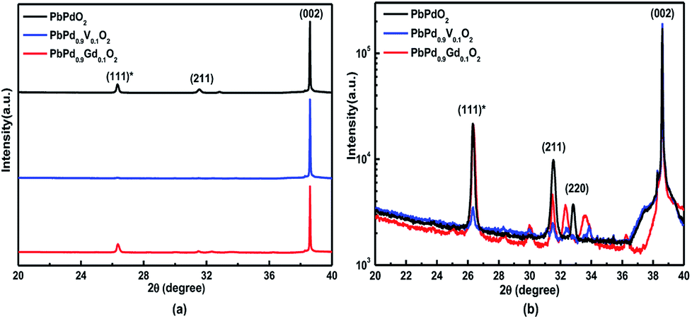 | ||
| Fig. 1 XRD patterns of PbPdO2, PbPd0.9V0.1O2 and PbPd0.9Gd0.1O2. (a) and (b) present the intensity and log intensity as a function of 2 theta, respectively. | ||
Fig. 2(a)–(f) shows the SEM images and AFM surface morphologies of PbPdO2, PbPd0.9V0.1O2, PbPd0.9Gd0.1O2 thin films, respectively. Fig. 3(a), (b) and (c) show the EDS spectra of PbPdO2, PbPd0.9V0.1O2, PbPd0.9Gd0.1O2 thin films, respectively. From Fig. 2(a), it can be found that the PbPdO2 thin film is composed of nanoparticles with a particle size of about 100 nm and the PbPd0.9V0.1O2 film contains many bar-like structures with width of 100–150 nm in Fig. 2(b). Moreover, Gd doping changes obviously the morphologies of the samples, and a lot of rod-like structures with the length of about 500 nm and width of about 100 nm are observed in Fig. 2(c). Moreover, from the surface morphologies in Fig. 2(d)–(f), the values of the surface roughness (Rq) are 52.4 nm, 92.2 nm and 90.7 nm for PbPdO2, PbPd0.9V0.1O2, PbPd0.9Gd0.1O2 thin films, which is consistent with the observed results from SEM. The sizes of PbPdO2, PbPd0.9V0.1O2 and PbPd0.9Gd0.1O2 thin films prepared by PLD technique are larger than those prepared by sol–gel spin coating.5,12 From the EDS measured results in Fig. 3, it is obtained that the atomic ratio of Pb![[thin space (1/6-em)]](https://www.rsc.org/images/entities/char_2009.gif) :Pd is 0.81:1.00 for PbPdO2; Pb:Pd:V atomic ratio is 0.60:1.00:0.18 for PbPd0.9V0.1O2; the atomic ratio of Pb:Pd:Gd is 0.57:1.00:0.18 for PbPd0.9Gd0.1O2. It should specially be noticed that the Mg signal in the EDS spectra is from the MgO substrate. From the measured results, we can deduce that there exist Pb vacancies in the three samples, which may be caused by the volatilization of Pb during the heating process. And the percentage of Pb vacancy in the samples also is changed due to the role of different ions. The measured results indicate that the percentage of Pb vacancy in PbPdO2 is the lowest, and the percentage of Pb vacancy in PbPd0.9Gd0.1O2 is the highest.
:Pd is 0.81:1.00 for PbPdO2; Pb:Pd:V atomic ratio is 0.60:1.00:0.18 for PbPd0.9V0.1O2; the atomic ratio of Pb:Pd:Gd is 0.57:1.00:0.18 for PbPd0.9Gd0.1O2. It should specially be noticed that the Mg signal in the EDS spectra is from the MgO substrate. From the measured results, we can deduce that there exist Pb vacancies in the three samples, which may be caused by the volatilization of Pb during the heating process. And the percentage of Pb vacancy in the samples also is changed due to the role of different ions. The measured results indicate that the percentage of Pb vacancy in PbPdO2 is the lowest, and the percentage of Pb vacancy in PbPd0.9Gd0.1O2 is the highest.
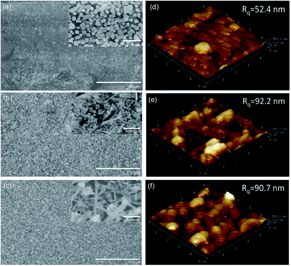 | ||
| Fig. 2 SEM surface images and AFM surface morphologies of PbPdO2 (a) and (d), PbPd0.9V0.1O2 (b) and (e) and PbPd0.9Gd0.1O2 (c) and (f). | ||
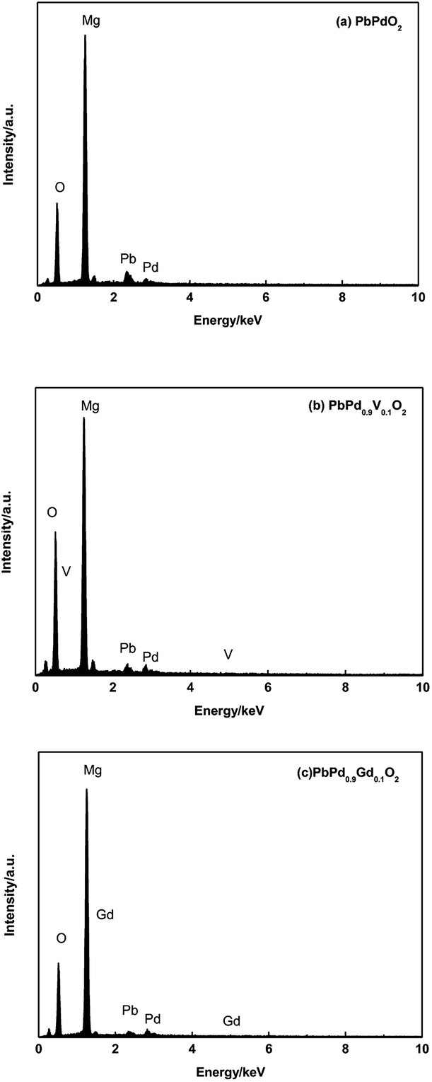 | ||
| Fig. 3 EDS spectra of PbPdO2 (a), PbPd0.9V0.1O2 (b) and PbPd0.9Gd0.1O2 (c). | ||
Fig. 4(a), (b) and (c) shows the XPS images of Pb 4f in PbPdO2, PbPd0.9V0.1O2 and PbPd0.9Gd0.1O2 films, respectively. From the figures, it is found that the XPS spectra of Pb 4f for three films can be divided into two pairs of characteristic peaks corresponding to Pb 4f5/2 and Pb 4f7/2, which is similarly to previous studied results.13 From Fig. 4(a), two pairs of characteristic peaks are described as following: main peaks (136.55 eV, 141.49 eV), and satellite peaks (137.50 eV, 142.20 eV); from Fig. 4(b), two pairs of characteristic peaks are described as following: main peaks (137.22 eV, 142.07 eV), and satellite peaks (138.05 eV, 142.88 eV); from Fig. 4(c), two pairs of characteristic peaks are described as following: main peaks (136.87 eV, 141.65 eV), and satellite peaks (137.75 eV, 142.50 eV). Clearly, with doping V and Gd, the sites and intensities of two pairs of peaks are changed, which means that doping has important role on ion vacancy and valence. The main peaks can be attributed to the lattice Pb of the samples, and the satellite peaks can be attributed to Pb vacancies.11 Moreover, the areas of main and satellite peaks for Pb 4f5/2 and Pb 4f7/2 in Fig. 4 were calculated. The calculated results indicate that the average area ratio of satellite peaks to total spectra (satellite + main peaks) are about 37.65%, 38.28% and 43.7% for Fig. 4(a), (b) and (c), respectively. Thus, it is obtained that Pb vacancies are about 37.65%, 38.28% and 43.7% for PbPdO2, PbPd0.9V0.1O2 and PbPd0.9Gd0.1O2 films, respectively. The above results are consistent with the results of EDS.
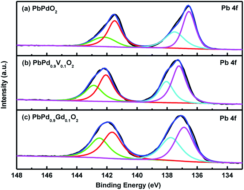 | ||
| Fig. 4 XPS spectra of Pb in PbPdO2 (a), PbPd0.9V0.1O2 (b) and PbPd0.9Gd0.1O2 (c). | ||
Fig. 5(a), (b) and (c) shows Pd 3d XPS images for PbPdO2, PbPd0.9V0.1O2 and PbPd0.9Gd0.1O2 thin films, respectively. From the figure, it is found that, both peaks for Pd 3d are symmetric and centered at around 336.28 eV and 341.59 eV for PbPdO2, around 336.09 eV and 341.51 eV for PbPd0.9V0.1O2, and around 336.10 eV and 341.51 eV for PbPd0.9Gd0.1O2, respectively. The two peaks stand for Pd 3d5/2 and Pd 3d3/2, which can be attributed to the formation of Pd2+.13,18,19
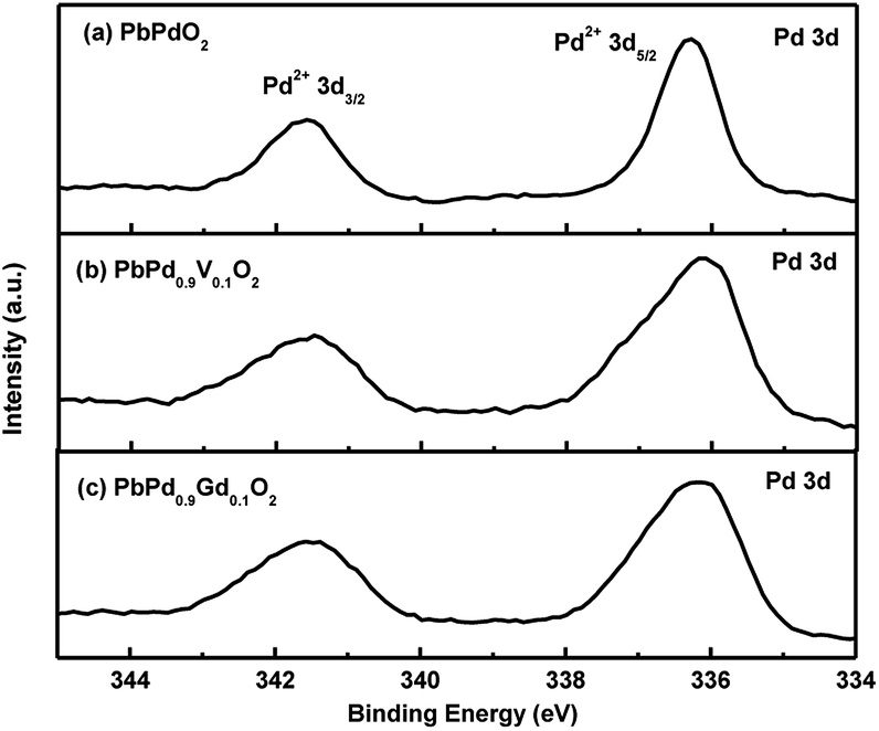 | ||
| Fig. 5 XPS spectra of Pd of PbPdO2 (a), PbPd0.9V0.1O2 (b) and PbPd0.9Gd0.1O2 (c). | ||
Fig. 6(a), (b) and (c) shows the XPS spectra of O 1s in PbPdO2, PbPd0.9V0.1O2 and PbPd0.9Gd0.1O2 films, respectively. From the figure, it can be seen that every O 1s spectrum can be divided into three peaks with one main peak I at about 528.93–529.39 eV and two satellite peaks II and III at about 530.80–531.01 eV and 532.83–533.80 eV. Moreover, the sites of main peak and satellite peaks are evidently influenced by V and Gd dopants. For PbPdO2, PbPd0.9V0.1O2 and PbPd0.9Gd0.1O2 films, the main peak can be attributed to the lattice O in PbPdO2, and the satellite peaks can be attributed to the oxygen and hydroxyl absorption on the surface of the sample.20,21 In particular, the peak III at about 532.83–533.8 eV should be related to the Pb vacancy, which can be explained as follows: since the Pb vacancy is generated, the valence of Pb is changed from +2 to +0, which makes the excess oxygen oxidized to O1−. As a result, O1− will absorb hydroxyl and CO2. Thus, the sample surface will be exposed in the atmosphere to absorb the hydroxyl and CO2.11 Compared with the doped samples, peak area percentage of II and III for the undoped sample is lowest. Thus, the content of Pb vacancies in undoped PbPdO2 is lowest. It is reasonable to deduce that ion doping can increase surface absorbed oxygen and Pb vacancy. V and Gd dopants increase the content of Pb vacancies. Especially, Gd doping makes PbPdO2 to produce most Pb vacancies. These results are consistent with the EDS those above.
 | ||
| Fig. 6 XPS spectra of O 1s in PbPdO2 (a), PbPd0.9V0.1O2 (b) and PbPd0.9Gd0.1O2 (c). | ||
Fig. 7(a) and (b) shows the XPS images of V and Gd in PbPd0.9V0.1O2 and PbPd0.9Gd0.1O2 films, respectively. From the Fig. 7(a), it can be seen that, two peaks at 515.70 eV and 516.80 eV should be corresponding to V4+ 2p3/2 and V5+ 2p3/2, respectively.22–24 V4+ and V5+ ions coexist in the V doping TiO2 has also been reported.25 At the same time, one can notices that the two peaks of Gd at about of 1186.86 eV and 1220.86 eV should be corresponding to Gd3+ 3d5/2 and Gd3+ 3d3/2.26,27
 | ||
| Fig. 7 XPS spectrum of (a) V 2p and (b) Gd 3d. | ||
Fig. 8(a), (b) and (c) show the M–H hysteresis loops for PbPdO2, PbPd0.9V0.1O2 and PbPd0.9Gd0.1O2 at room temperature, respectively. From Fig. 8, it is found that three samples have all ferromagnetism at room temperature. The saturation magnetization of PbPdO2, PbPd0.9V0.1O2 and PbPd0.9Gd0.1O2 were about 2.0 emu cm−3, 5.0 emu cm−3 and 8.0 emu cm−3, respectively. Obviously, V and Gd dopants improve magnetic moment of PbPdO2, and enhancing effect of Gd dopant is largest. The source of magnetism is generally related to its defects, the carrier concentration, and the valence of the dopant ions for metal oxides.28–30 Although, there exist very little impurity PdO and Gd2O3 phases in PbPd0.9V0.1O2 and PbPd0.9Gd0.1O2, these impurity phases do not contribute to ferromagnetism. Based on the above EDS and XPS measured results, one can notice that, the Pb vacancy, Pd2+ and O1− exist in PbPdO2. In theory, the effective spin magnetic moment of Pd2+ is zero. The magnetism of PbPdO2 film should result from O1−. Here, O1− is produced due to the presence of Pb vacancies, and 2p5 in O1− will lead to 1μB effect magnetic moment. Moreover, the valence states of V and Gd ions were confirmed to be V4+, V5+ and Gd3+ by XPS. For PbPd0.9V0.1O2, V4+ can contribute 1μB magnetic moment and V5+ makes no contribution. Therefore, the enhanced magnetism results from V doping. By contrast, Gd3+ can contribute 7μB magnetic moment. Thus, Gd doping increases evidently the magnetism of PbPd0.9Gd0.1O2. Fig. 9 shows the calculated spin DOSs of PbPdO2, PbPd0.9V0.1O2 and PbPd0.9Gd0.1O2 with Pb vacancy. The calculated results indicate that, the magnetic moment of PbPdO2 with Pb vacancy is 2.8μB, as shown in Fig. 9(a). As seen in Fig. 9(b) and (c), V dopant makes the magnetic moment to enhance to 6.5μB, and further Gd doping leads to the largest magnetic moment with 12.3μB. The doping role of the above magnetic moments explains well the experimental results in Fig. 8.
 | ||
| Fig. 8 M–H curves at room temperature of PbPdO2 (a), PbPd0.9V0.1O2 (b) and PbPd0.9Gd0.1O2 (c). | ||
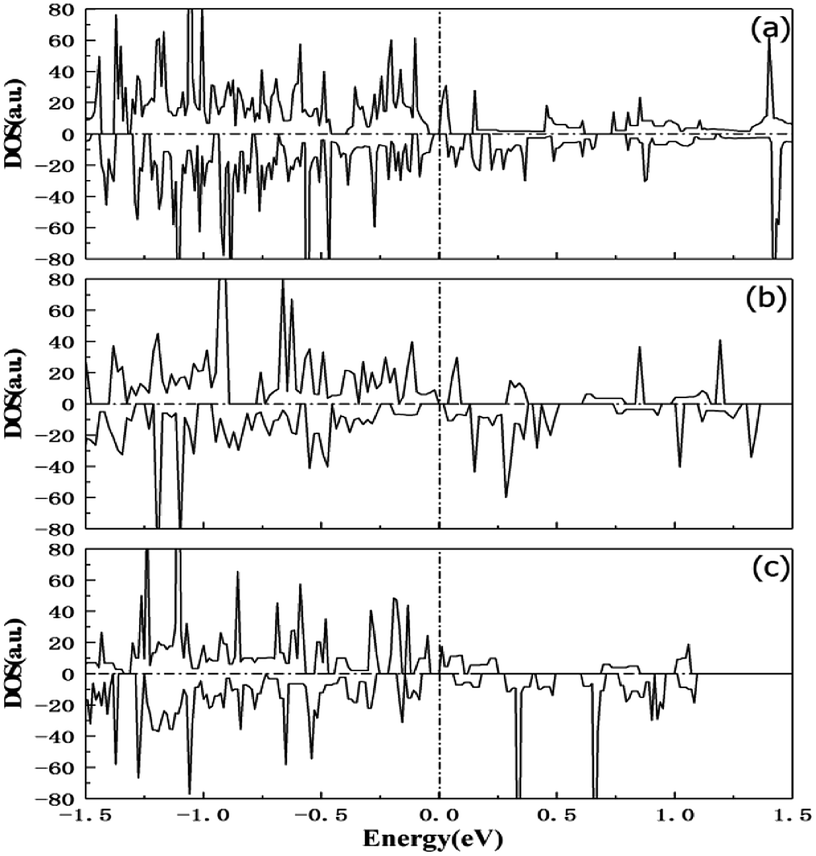 | ||
| Fig. 9 The calculated spin DOSs of PbPdO2 (a), PbPd0.9V0.1O2 (b) and PbPd0.9Gd0.1O2 (c). | ||
Fig. 10(a)–(c) shows the magnetization as a function of the temperature under zero-field cooling (ZFC) and field cooling (FC) for PbPdO2, PbPd0.9V0.1O2 and PbPd0.9Gd0.1O2 thin films. As the temperature is changed from 370 K to 70 K, the ZFC and FC curves gradually separated. As the temperature is larger about 375 K, the FC and ZFC curves tended to coincide, and the crosspoint is named as blocking temperature. The evident deviation between the FC and ZFC curves indicates that superparamagnetism and ferromagnetism can coexist PbPdO2, PbPd0.9V0.1O2 and PbPd0.9Gd0.1O2 thin films. These results are consistent with the previous report.5
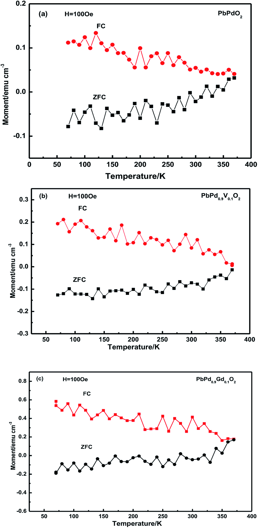 | ||
| Fig. 10 ZFC–FC M–T curves of PbPdO2 (a), PbPd0.9V0.1O2 (b) and PbPd0.9Gd0.1O2 (c) thin films. | ||
Fig. 11 exhibits the temperature dependence of the DC electrical resistivity (ρ). It can be seen from the figure that the resistivities of PbPdO2, PbPd0.9V0.1O2 and PbPd0.9Gd0.1O2 at room temperature are 0.179 Ω cm, 0.389 Ω cm and 0.143 Ω cm, respectively. Compared with the bulk resistivity,3 these values become less. In addition, it is found that the resistivity of PbPd0.9V0.1O2 is larger than that of PbPdO2, and the resistivity of PbPd0.9Gd0.1O2 is smaller than that of PbPdO2. This indicates that different ion doping has a significant effect on the physical properties of PbPdO2. To analyze the resistivity change produced by ion doping, the carrier densities and mobilities at room temperature for three films were measured, and the results are as following: for PbPdO2, the hole-type carrier density and mobility is 5.56 × 1017 cm−3 and 2.22 × 104 cm2 V−1 s−1, respectively; for PbPd0.9V0.1O2, they are 1.0 × 1017 cm−3 and 20.2 × 104 cm2 V−1 s−1; for PbPd0.9Gd0.1O2, they are 26.9 × 1017 cm−3 and 7.1 × 104 cm2 V−1 s−1, respectively. Obviously, the resistivity change produced by ion doping can be explained by difference of the carrier density. To clarify the role of vacancy and dopant on the resistivity, we have also carried out first-principles calculations. From the calculated spin-polarized DOSs of PbPdO2, PbPd0.9V0.1O2 and PbPd0.9Gd0.1O2 in Fig. 9, one can find that V and Gd dopants have clear role on the band gap. From Fig. 9(a), the presence of Pb vacancies results in a band gap of 0.028 eV in PbPdO2. After the further doping of Gd and V atoms, we found distinct effects on the band gap: the introduction of Gd3+ reduces the band gap to 0.019 eV, while the doping of V4+,5+ increases the band gap to 0.036 eV. The above calculated results reveal well the variation of electrical resistivity for three samples as shown in Fig. 11.
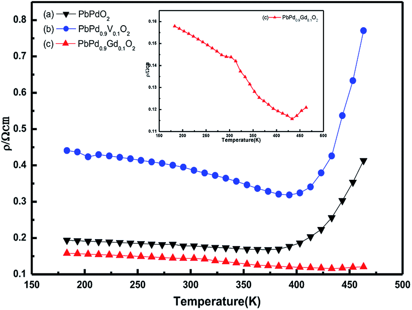 | ||
| Fig. 11 Temperature dependence of DC electrical resistivity for PbPdO2, PbPd0.9V0.1O2 and PbPd0.9Gd0.1O2 thin films. The inset shows the magnified temperature dependence of resistivity of PbPd0.9Gd0.1O2 thin film. | ||
The electron transport in PbPdO2 is controlled by hole carriers through the Pd–O hybridization, and the doping of Gd ions can make the Pd–O hybrid stronger, while the doping of V ions weaken the Pd–O hybridization. Therefore, ion doping significantly changes the conductivity of the sample. In addition, it is found that there is a significant insulator–metal transition temperature in the samples. The insulator–metal transition temperatures for PbPdO2, PbPd0.9V0.1O2 and PbPd0.9Gd0.1O2 are respectively about 385 K, 390 K, 430 K, which is much higher than previous experimental reports.2,4 Significant differences in TMI may be related to microstructural differences arising from different preparation conditions.
Conclusions
PbPdO2, PbPd0.9V0.1O2 of PbPd0.9Gd0.1O2 films with the preferred orientation of (002) have been synthesized by PLD technique. The particle size and surface roughness of three films were obtained by SEM and AFM measurements. Moreover, the valence states for Pb, Pd, O, Gd and V ions were found to be 2+, 2+, 2−, 3+ and the mixed 4+ and 5+, respectively. Meanwhile, it is found that three samples have Pb vacancies and room temperature ferromagnetism. The saturation magnetization of PbPdO2, PbPd0.9V0.1O2 and PbPd0.9Gd0.1O2 were found to be about 2.0 emu cm−3, 5.0 emu cm−3 and 8.0 emu cm−3, respectively. Moreover, the temperature dependence of resistivity indicates that, the electrical resistivity is enhanced by V ion substitution, but being weakened by Gd ion substitution. Significant insulator–metal transition temperatures were also observed. Finally, based on the calculated spin DOSs of PbPdO2, PbPd0.9V0.1O2 and PbPd0.9Gd0.1O2 with Pb vacancy, the magnetic origin of three samples, and V (Gd) doping roles on the electrical and magnetic properties can be explained well.Conflicts of interest
There are no conflicts to declare.Acknowledgements
This work is supported by the National Science Foundation of China (61574037, 61404029, 11404058, 11274064); Natural Science Foundations of Fujian Province of China (Grant No. 2017J06001).Notes and references
- X.-L. Wang, S. X. Dou and C. Zhang, NPG Asia Mater., 2010, 2(1), 31–38 CrossRef.
- T. C. Ozawa, T. Taniguchi, Y. Nagata, Y. Noro, T. Naka and A. Matsushita, J. Alloys Compd., 2005, 388, 1–5 CrossRef CAS.
- X. L. Wang, Phys. Rev. Lett., 2008, 100, 3136–3140 Search PubMed.
- X. L. Wang, G. Peleckis, C. Zhang, H. Kimura and S. X. Dou, Adv. Mater., 2009, 21, 2196–2199 CrossRef CAS.
- H. L. Su, S. Y. Huang, Y. F. Chiang, J. C. A. Huang, C. C. Kuo, Y. W. Du, Y. C. Wu and R. Z. Zuo, Appl. Phys. Lett., 2011, 99, 102508 CrossRef.
- S. M. Choo, K. J. Lee, S. M. Park, G. S. Park and M. H. Jung, J. Appl. Phys., 2013, 113, 014904 CrossRef.
- S. M. Choo, K. J. Lee, S. M. Park, J. B. Yoon, G. S. Park, C.-Y. You and M. H. Jung, Appl. Phys. Lett., 2015, 106, 172404 CrossRef.
- K. J. Lee, S. M. Choo, J. B. Yoon, K. M. Song, Y. Saiga, C.-Y. You, N. Hur, S. I. Lee, T. Takabatake and M. H. Jung, J. Appl. Phys., 2010, 107, 09C306 CrossRef.
- K. J. Lee, S. M. Choo and M. H. Jung, Appl. Phys. Lett., 2015, 106, 072406 CrossRef.
- K. J. Lee, S. M. Choo, Y. Saiga, T. Takabatake and M. H. Jung, J. Appl. Phys., 2011, 109, 07C316 CrossRef.
- X. Chen, Y. Chen, Y. M. Yang, H. Jia, J. M. Zhang, S. Y. Chen and Z. G. Huang, Ceram. Int., 2017, 43, 10428–10433 CrossRef CAS.
- J. Liu, C. Mei, P. Y. Chuang, T. T. Song, F. L. Tang, H. L. Su, J. C. A. Huang and Y. C. Wu, Ceram. Int., 2016, 42, 15762–15766 CrossRef CAS.
- F. L. Tang, J. Liu, C. Mei, S. Y. Huang, T. T. Song, H. L. Su, M. K. Lee, Y. C. Wu and J. C. A. Huang, RSC Adv., 2016, 6, 37522–37529 RSC.
- G. Kresse and J. Hafner, Phys. Rev. B: Condens. Matter Mater. Phys., 1993, 48, 13115–13118 CrossRef CAS; G. Kresse and J. Furthmüller, Phys. Rev. B: Condens. Matter Mater. Phys., 1996, 54, 11169 CrossRef.
- P. E. Blöchl, Phys. Rev. B: Condens. Matter Mater. Phys., 1994, 50, 17953 CrossRef.
- G. Kresse and J. Furthmüller, Comput. Mater. Sci., 1996, 6, 15 CrossRef CAS.
- J. P. Perdew, K. Burke and M. Ernzerhof, Phys. Rev. Lett., 1996, 77, 3865 CrossRef CAS PubMed.
- K. C. Lee, Y. J. Chiang, Y. C. Lin and F. M. Pan, Sens. Actuators, B, 2016, 226, 457–464 CrossRef CAS.
- M. Brun, A. Berthet and J. C. Bertolini, J. Electron Spectrosc. Relat. Phenom., 1999, 104, 55–60 CrossRef CAS.
- H. Q. Zhao, J. Wang, L. X. Zhang, Y. C. Rong, J. Chen, K. Ibrahimb and X. R. Xing, Dalton Trans., 2013, 42, 10358–10364 RSC.
- S. Takatani, H. Miki, K. Kushida-Abdelghafar and K. Torii, J. Appl. Phys., 1999, 85, 7784–7791 CrossRef CAS.
- J. Xu, C. X. Qin, Y. L. Huang, Y. R. Wang, L. Qin and H. J. Seo, Appl. Surf. Sci., 2017, 396, 1403–1410 CrossRef CAS.
- R. Larsson, B. Folkesson and G. Schoen, Chem. Scr., 1973, 3, 88 CAS.
- V. I. Nefedov, M. N. Firsov and I. S. Shaplygin, J. Electron Spectrosc. Relat. Phenom., 1982, 26, 65 CrossRef CAS.
- F. Z. Ren, H. Y. Li, Y. X. Wang and J. J. Yang, Appl. Catal., B, 2015, 176, 160–172 CrossRef.
- Y. Uwamino, Y. Ishizuka and H. Yamatera, J. Electron Spectrosc. Relat. Phenom., 1984, 34, 69 CrossRef.
- D. Raiser and J. P. J. Deville, J. Electron Spectrosc. Relat. Phenom., 1991, 57, 91 CrossRef CAS.
- A. Sundaresan and C. N. R. Rao, Nano Today, 2009, 4(1), 96–106 CrossRef CAS.
- S. B. Ogale, Adv. Mater., 2010, 22(29), 3125–3155 CrossRef CAS PubMed.
- T. Dietl, Nat. Mater., 2010, 9(12), 965–974 CrossRef CAS PubMed.
| This journal is © The Royal Society of Chemistry 2018 |