DOI:
10.1039/C8RA07955B
(Paper)
RSC Adv., 2018,
8, 39241-39247
Characteristics of microcontact printing with polyelectrolyte ink for the precise preparation of patches on silica particles†
Received
25th September 2018
, Accepted 15th November 2018
First published on 23rd November 2018
Abstract
This publication demonstrates the abilities of a precise and straightforward microcontact printing approach for the preparation of patchy silica particles. In a broad particle size range, it is possible to finely tune the number and parameters of three-dimensional patches like diameter and thickness using only polyethyleneimine ink, poly(dimethoxysilane) as stamp material and a suitable release solvent.
Introduction
The advantages and possibilities of anisotropic colloids and their self-assembly have extensively been described in the literature.1,2 Examining the various synthetic methods for these nano- and microscopic building blocks shows an exceptional wealth of ideas and creativity: interface chemistry at the boundary of two immiscible phases produces anisotropic colloids by the partial functionalization of the particle surface while controlling the patch balance.3 The assembly of triblock terpolymers yields soft patchy nanoparticles, which are able to undergo further ordering on a higher hierarchical level.4 Inorganic films can be deposited onto particles using physical vapour deposition, influencing the patch size by adjusting the incident angle, or by using a flow-through nucleation and grow mechanism.5–7 Polyelectrolyte solutions are used in a dip coating process to produce thin patches on colloids.8 Solid templates shield the particle surface from modification with nanoparticles with a tuneable coverage, or the complete coating with organic films and the subsequent partial exposure via plasma etching allows the functionalization of mono- and bifunctional particles.9,10 Between all these methods the microcontact printing approach still exhibits a fascinating accessibility for the direct surface modification of organic or inorganic colloids.11–15 This strategy was used for both, printing sophisticated polymer systems onto organic particles and the direct surface modification of silica particles with silanes.16,17 The latter was further used to modify the particle surface directly with ATRP initiators, subsequently starting a polymerization of multifunctional polymer patches.18
We recently reported a new strategy for the accurate production of 5 μm patchy silica particles using microcontact printing (μCP) with polyethyleneimine ink (PEI) and poly(dimethoxysilane) stamps (PDMS).19,20 We outlined the possibility of switching between two-dimensional modification (2D) and three-dimensional structures (3D) by simple alteration of solvent during particle release and discussed the underlying physical mechanism. We furthermore used the volume of the obtained patches for the incorporation of functional nanoadditives, without altering the patch surface chemistry, and post modification of said patches leading to supramolecular self-assembly. Previous investigations showed different ways to manipulate the patch diameter during μCP by changing stamp stiffness, pressure and reaction time between the particle surface and molecular ink.16,21 While all these concepts possess certain benefits, the possibility of printing 3D structures onto the particle surface had not been shown before, let alone to change the patch thickness in a single μCP step. In our approach we renounce the mentioned techniques but use an easier and more convenient way of changing the patch geometry at a constant printing force by using polymeric inks. The advantage of polymeric inks is the nearly complete absence of ink diffusion, which is a common problem for molecular inks, as well as the ability to change the ink film thickness on the PDMS stamp to ultimately control the patch diameter and thickness.22,23 As an ideal counterpart for the negatively charged silica surface we selected the polyelectrolyte PEI.24–27 With its high density of positively charged amine groups, and therefore its potential for additional modification steps, it possess a very strong electrostatic bonding to the particle surface and is a perfect starting material for covalent or supramolecular self-assembly experiments.19
During our investigations we further improved this new 3D μCP method by greatly broadening the particle size range while still being able to vary the patch geometry for single patched particles (SPP). Following this, we investigated the influence of the synthetically given particle size distribution of used silica spheres on the patch diameter. By using simple assumptions, we were able to obtain an evaluation of the accruing error margins, given better quality estimation for our achieved results. We were further able to expand our concept to double patched particles (DPP), meaning a particle with two patches on opposite sides (180° angle). While ‘‘sandwich’’ printing is a typical tool for the modification with molecular inks which covalently attach to the particle surface, it is a nontrivial task for our electrostatic approach leading to a slightly modified printing procedure and patch geometries.28 Finally, we compare key parameters for characterization of achieved patches and discuss differences between SPP and DPP results.
Results and discussion
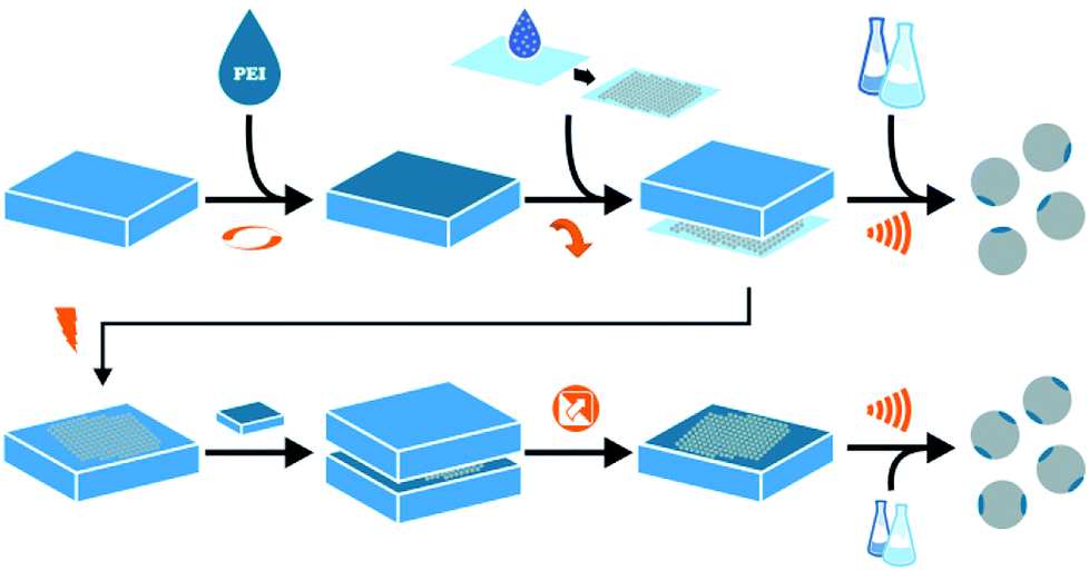
Fig. 1 illustrates our μCP approach starting in the top row for SPP![[thin space (1/6-em)]](https://www.rsc.org/images/entities/char_2009.gif) :PDMS stamps are loaded with aqueous PEI solutions using spin coating. The thickness of the PEI film is adjusted by changing the concentration of said solutions. During this research four thicknesses were used (25 nm, 50 nm, 85 nm, 127 nm). Particle monolayers are produced by drop casting alcoholic dispersions onto cleaned glass. During the printing process, a loaded PDMS stamp is softly pressed onto the particle monolayer, using the same printing force for all samples, and directly removed from the glass substrate.19 Finally, the particle-covered PDMS stamps are immersed into a suitable solvent and the patchy particles are released from the stamp using ultra-sonification.
:PDMS stamps are loaded with aqueous PEI solutions using spin coating. The thickness of the PEI film is adjusted by changing the concentration of said solutions. During this research four thicknesses were used (25 nm, 50 nm, 85 nm, 127 nm). Particle monolayers are produced by drop casting alcoholic dispersions onto cleaned glass. During the printing process, a loaded PDMS stamp is softly pressed onto the particle monolayer, using the same printing force for all samples, and directly removed from the glass substrate.19 Finally, the particle-covered PDMS stamps are immersed into a suitable solvent and the patchy particles are released from the stamp using ultra-sonification.
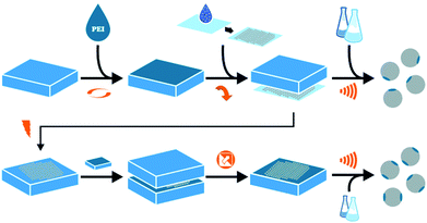 |
| | Fig. 1 Scheme displays microcontact printing approach for single (SSP) and double patched particles (DPP) in top and bottom row respectively. From left to right: production of PDMS stamps loaded with differently concentrated PEI solutions; drop casting of silica particle dispersion for monolayer creation; printing process and particle release from stamp using ultrasonic treatment in a suitable solvent. For DPP additional plasma treatment step, repetition of printing step and particles release from the second PDMS stamp. | |
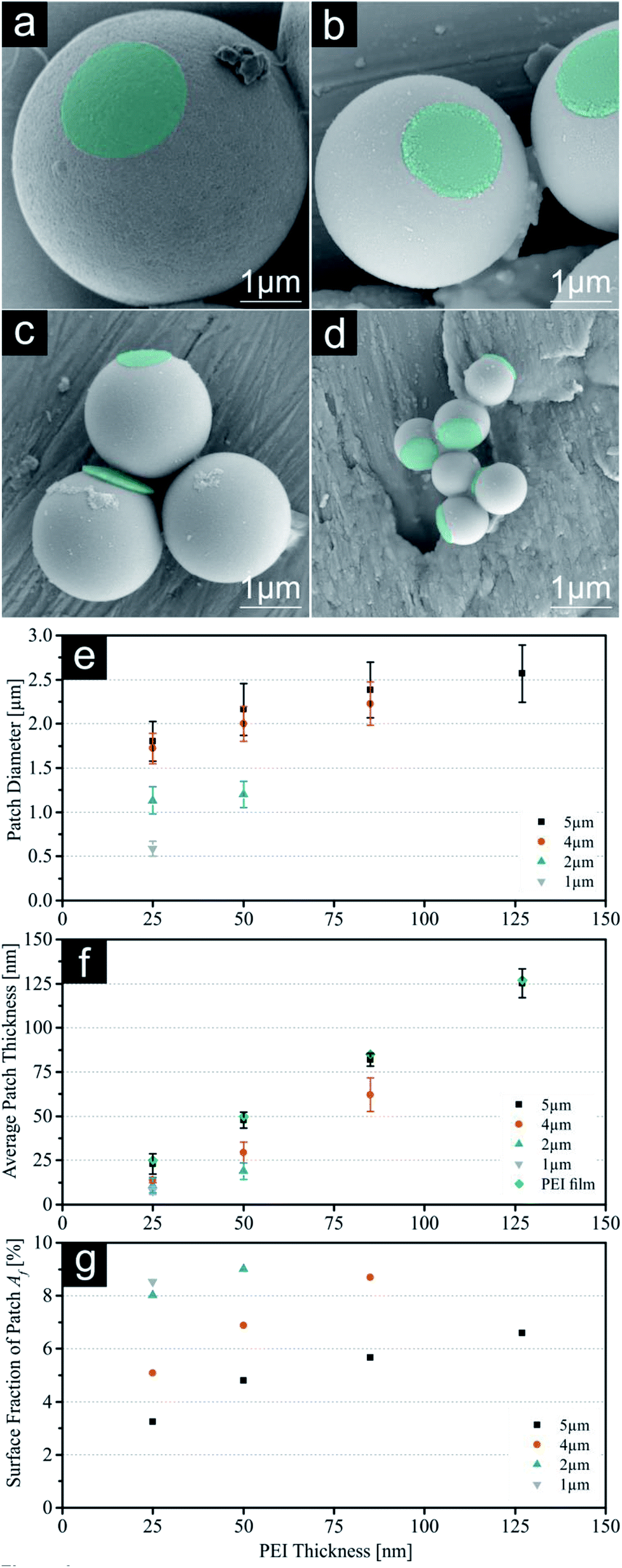
We used several analytical methods to investigate the quality of the resulting SPP and measured different parameters: scanning electron microscopy (SEM) images give a clear image of the structure and geometrical form of the obtained 3D patches. Fluorescence microscopy (FM) and labelling of the printing patches was used to check the composition and to calculate an average patch diameter d. Scanning force microscopy (SFM) was used as an indirect measurement on the dried PDMS stamps after particle release to receive the average patch thickness t from formed holes left on the stamp and to compare them with the initial film thickness of the PEI.
Single patched particles (SPP)
First, our results concerning single patched particles with a size of 5, 4, 2 and 1 μm will be discussed. As previously reported, the largest SPP were successfully printed with all four PEI thicknesses giving it a broad range of different patch sizes.19 Printing of higher thicknesses of PEI onto smaller silica particles resulted in an insufficient amount of achieved patchy particles, because the thickness of the polymeric film reaches a certain threshold where it is too thick to release the printed particles. As a result of this, no particles were visible for these samples during microscopic evaluation using similar release times. For these conditions' particles remained attached to the loaded PDMS stamp. Consequently, smaller particles were only printed with ink films enabling adequate particle yields (e.g. 4 μm particles with 25 nm, 50 nm, 85 nm PEI). SEM images of all SPP sizes printed with the lowest PEI thickness (25 nm) and diagrams summarizing the calculated patch parameters are shown in Fig. 2. Additional SEM (without colouring), FM and SFM images for all particle sizes and higher PEI thicknesses and particles yield for SPP can be found in the ESI (Fig. S1–S4, S9–S12 and Table S7†). The 5 μm particles exhibit a t value almost identical to the measured thickness of the PEI film on the stamps, which was deduced by analysing the PEI film thickness after spin coating on a silica wafer model system and ensuing scratching of the ink film. These measurements give a theoretical maximum for the reachable patch thickness on the silica particles, which is obviously completely transferred onto the particle surface during the release mechanism of 5 μm spheres.19 Smaller particles do not show this correlation, but a systematic decline of the average patch thickness with decreasing particle size. Simple calculations of the particle density for the silica monolayer with different particle diameters show a plausible explanation for this behaviour (compare Fig. S18†). While applying the same printing force onto all systems, the contact area between the particle surfaces and polymer film increases with decreasing particle size, because the particle density increases. Due to this the printing pressure for each individual particle decreases with decreasing particle diameter. The calculated absolute (P) and relative printing pressures (Pr) are displayed in Table 1. For this reason, it is suggested, that smaller particles show thinner patch geometry, as the particles are not completely submerged into the polymeric film on the stamp. At this point we would like to mention, that the presented t data should be understood as an average thickness value for the patch thickness. SEM images clearly show an uneven distribution of the PEI along the patch (compare ESI†). This is a result of two different effects, which will most probably occur simulations during the particle printing:
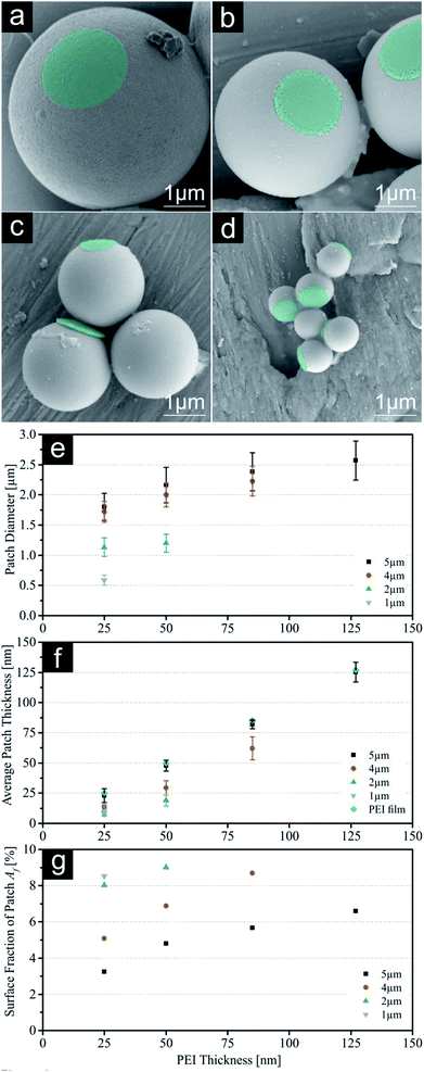 |
| | Fig. 2 (a–d) SEM images with constant scale of single patched particles (SPP, printed with 25 nm PEI) with decreasing sizes (5 μm, 4 μm, 2 μm & 1 μm). Images of PEI patches were subsequently coloured for better visualization. (e) Patch diameter d measured with fluorescence microscopy. (f) Indirect measurement of the average patch thickness t using SFM on the PDMS stamps after release. (g) Calculated surface fraction of patch Af. For values see ESI.† Error bars represent standard deviation. | |
Table 1 Table shows the calculated values for absolute P and relative printing pressures Pr for all particles during microcontact printing at constant printing force with changing particle size (see ESI Fig. S18).19
| Particle size |
5 μm |
4 μm |
2 μm |
1 μm |
| P |
889 kPa |
718 kPa |
375 kPa |
181 kPa |
| Pr |
100% |
81% |
42% |
20% |
First, the particle penetration into the PEI during printing. The ink film under the particle will be inhomogeneously deformed (especially strong beneath the particle pole) and therefore pressed out around the immersed segment of the particle surface. After particle release, this results in a lower patch thickness in its centre and higher in its outer regions, respectively. Second, the PDMS is not a hard substrate and will therefore sag in upon the pressure imposed by the printed particle. This will lead to the formation of concave contact areas between the PDMS stamp, the ink film and the particle surface and further to the uneven patch thickness and to its not flat but rather convex geometry. In good agreement with this, holes in the PEI film on the PDMS stamps seem to be quite uniform in thickness (compare ESI†), conforming the almost complete transfer of polymer ink to the particle surface. As a consequence of both effects, measured d values will be higher in comparison to theoretical calculations for them, which will be discussed in the following section.
Nevertheless, the resulting t values for all particle systems are still high enough to identify these patches as 3D structures rather than a 2D surface functionalization, which we presented previously.19 Fig. 2g shows the calculated surface fractions of the patch Af. With this system we can cover a range of 3% to 9% (25 nm on 5 μm and 50 nm on 2 μm respectively). This parameter is important for future self-assembly experiments as it gives us a tool to precisely adjust the Janus balance of particles.29–31 To confirm the electrostatic bonding between the silica particle surface and the PEI, additional pH-dependant experiments were carried out. Remarkably the patches show a good adhesion to a particle's surface even in aqueous solutions in a pH-range between 3 and 11. Beyond this range the detachment of the polymer patches from the particle surface is observed, due to the protonation of the silica surface or deprotonation of the PEI respectively. Surprisingly, the patches did not dissolve but remain stable in spite of good water solubility of PEI and labelled patches are clearly visible via FM (see Fig. S17†).
Influence of particle size distribution
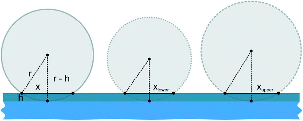
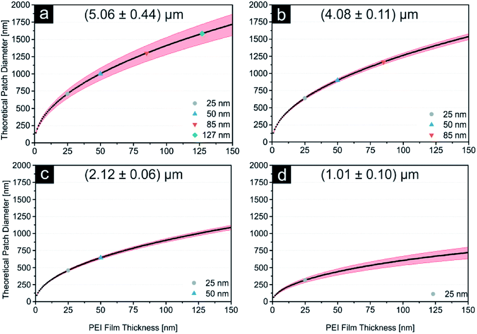
As displayed in Fig. 2e and Table 2, the error margin for the patch diameter reaches high values of up to ±0.32 μm and is varying strongly for different particle sizes. It should be mentioned, that the results and error margins are calculated as mean values for multiple printing experiments for all particle sizes and ink film thicknesses. Therefore, an evaluation of the high reproducibility of this process is included in these values. Still, this did not reach our self-imposed goal and further investigations concerning this quality factor were conducted. Since all synthesized colloids possess a certain particle size distribution, we aimed to calculate the influence of this factor on the patch diameter during microcontact printing. Fig. 3 illustrates the concept and the used variables for this evaluation. To simplify this calculation harshly we hypothesized two points: firstly, the particles completely penetrated the polymer film without altering the film surface. And secondly, no bending of the PDMS was considered. As these two factors are difficult to quantify in a simple mathematical model, it was necessary to discard them. These substantial simplifications generate a lowest possible influence of the size distribution during printing and will not represent a real printing result. For that reason, it is not feasible to predict actual patch diameters with this model. Diagrams in Fig. 4 display the calculated functions, highlighted theoretical error margins of the patch diameter and the values corresponding to our experimental data are given in Table 3. It is clearly visible that the particle size distribution can contribute significantly to the measured error margin for the patch diameter. The contribution of the particle size distribution on the measured errors of d for the 5 μm silica spheres lies between 59% and 88% and is therefore the main influence for the broadening of the patch diameter. The usage of a perfectly monodisperse particle sample would lead to a considerable decrease of the error margin and reveal the true potential of this approach. At this point it is to be reminded, that this model does not consider the elasticity of the stamping material. For that reason, the calculated absolute values of d are significantly lower in comparison to the experimental values. Bending of the stamp and the viscosity of the polyelectrolyte ink do influence the overall geometry of the patches (e.g. Fig. S2c†). For the future, we aim to give a more sophisticated model of our experimental observations. Furthermore, it is most likely, that the influence of the particle size distribution will be even higher due to bending and polymer movement during particle penetration into the ink film, further increasing the error margins.
Table 2 Measured patch diameter d with calculated standard deviation for single patched particles (SPP) including results for all particles sizes and applicable ink film thicknesses during microcontact printing
| PEI thickness |
d5 μm [μm] |
d4 μm [μm] |
d2 μm [μm] |
d1 μm [μm] |
| 25 nm |
1.80 ± 0.22 |
1.72 ± 0.17 |
1.13 ± 0.15 |
0.59 ± 0.08 |
| 50 nm |
2.16 ± 0.29 |
2.00 ± 0.20 |
1.20 ± 0.15 |
|
| 85 nm |
2.38 ± 0.31 |
2.23 ± 0.25 |
|
|
| 127 nm |
2.57 ± 0.32 |
|
|
|
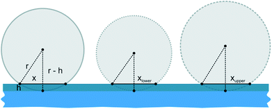 |
| | Fig. 3 Illustration of silica particles with average size value (solid line) accompanied by the upper (striped line) and lower (dotted line) size distribution limit. Particles penetrate the ink film completely. The sketch should clarify the used model and variables for calculating the influence of particle size distribution on the experimentally measured patch diameter. A larger particle leads in conclusion to a larger patch diameter, which would alter the achieved precision. | |
 |
| | Fig. 4 (a–d) The influence of the particle size distribution on the patch diameter is displayed here as the theoretical patch diameter is plotted as a function of the polymer film thickness for (5.06 ± 0.44) μm, (4.08 ± 0.11) μm, (2.12 ± 0.06) μm and (1.01 ± 0.1) μm particles. Red areas highlight the influence of the size distribution. Film thicknesses corresponding to the polymer solutions used experimentally are highlighted in different colours (compare ESI). | |
Table 3 Theoretically calculated error e describing the influence of the particle size distribution for different particles sizes on the patch diameter, which was obtained using a simplified evaluation (compare Fig. 3 and ESI S16). Results show how size distribution contributes to a significant extent of the patch diameter broadening
| PEI thickness |
e5 μm [μm] |
e4 μm [μm] |
e2 μm [μm] |
e1 μm [μm] |
| 25 nm |
0.13 |
0.04 |
0.03 |
0.07 |
| 50 nm |
0.18 |
0.08 |
0.04 |
|
| 85 nm |
0.23 |
0.12 |
|
|
| 127 nm |
0.28 |
|
|
|
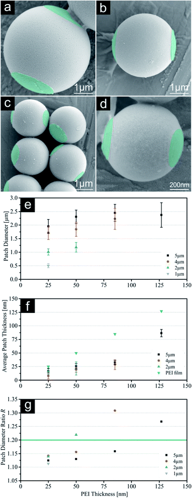 |
| | Fig. 5 (a–d) SEM images of double patched particles (DPP, printed with 25 nm PEI) with decreasing sizes (5 μm, 4 μm, 2 μm & 1 μm). PEI patches were subsequently coloured for better visualization. (e) Patch diameter d measured with fluorescence microscopy. (f) Indirect measurement of the average patch thickness t using AFM on the PDMS stamps after release. (g) Calculated patch size ratio R. For values see ESI.† Error bars represent standard deviation. | |
Double patched particles (DPP)
The increase of patch number was investigated to create trivalent patchy particles with this approach. The generation of DPP proved to be a rather difficult task for our system considering the particle release using ultra-sonication to be the most important step for 3D patches. Experiments without additional adaptation and two consecutive printing steps led almost exclusively to SPP. Hereby particles were removed from the first stamp without attachment of any PEI. Attempts keeping the substrates connected during particle release proven to be unsuccessful with almost no distinct patches visible during FM investigations.
However, we were able to introduce a simple air plasma etching step prior to the second printing step (see Fig. 1 bottom row). With this, the polymeric ink in between the particles is carefully removed, leading to a reduced contribution of the lateral component of the adhesion force during lift-off with the second PDMS stamp. This approach opens the way for the generation of symmetrical patchy particles with three-dimensional structures. Fig. 5 displays SEM images of all DPP sizes printed with 25 nm PEI from both sides and diagrams summarizing the patch parameters (d, t, R). All parameters have been calculated as an average for both patch sides. Respective images (SEM, FM, SFM) and particles yield for DPP can be found in the ESI (Fig. S5–S8, S9–S12 and Table S7†). The average patch thicknesses t were compared with results for SPP showing a significant decrease of corresponding values. This finding could be explained by two reasons: first, due to the removal of PEI from the first PDMS stamp during plasma etching, the values obtained by SFM are decreased as it gives the height difference between the top of the polymer ink film and the bottom of the remaining holes. Second, printing is conducted using two soft substrates in contrast to the glass/PDMS combination for SPP. Using the same printing force in all experiments a softer stamp material leads to a damping of printing pressure for the individual DPP and a reduced penetration depth into the polymeric ink film will occur. In general, the course of the patch diameter is similar showing reduced values for the DPP, but we examined a strong increase in the error margin for the highest PEI thickness. Accordingly, we calculated the diameter ratio R between the smaller and larger patch for all samples. At lower thicknesses we observe ratios between 1.12 and 1.16 demonstrating a good symmetry, but thicker PEI films lead to values up to 1.31. These samples show a clear size difference between the first and second patch, hence increasing the error margin for the patch diameter greatly. We chose a ratio smaller than 1.2 to be a sufficient quality for DPP. However, this effect can be used deliberately to generate asymmetric patchy particles and may even be finely controlled by using two stamps loaded with different PEI thicknesses.
Conclusions
In conclusion, we have developed a method for the precise generation of single and double patched silica particles in a broad size range using a simple microcontact printing approach with PDMS stamps and PEI as polymeric ink. PEI is used as a positively charged polyelectrolyte creating a strong and stable electrostatic bond to the negative silica surface which, if necessary, can be cleaved by increasing or decreasing the pH value beyond the isoelectric point of one of both materials. Geometrical patch parameters like average diameter, thickness and patch area are finely tuneable for all particle sizes and were studied in detail using FM and SFM. With the possibilities of simple post modification of the PEI patches, we achieved the versatile toolbox for precise self-assembly experiments using colloidal building blocks with highly controllable parameters.
Materials and methods
Chemicals
Poly(dimethylsiloxane) (PDMS) was prepared from Sylgard 184 elastomer kit obtained from Dow Corning. 50 wt% aqueous solutions polyethyleneimine (PEI) was purchased from Fluka Chemicals with a molecular weight distribution from 600 to 1000 kg mol−1. Dry silica particles with a size of (5.06 ± 0.44) μm and (1.01 ± 0.1) μm were purchased from Bang Laboratories, with a size of (4.08 ± 0.11) μm from Cospheric and particles in aqueous solution with a size of (2.12 ± 0.06) μm from microparticles. Ethanol was purchased from Th. Geyer (reinst) and acetone from VWR (ACS reagent). Fluorescein isothiocyanate (FITC) was obtained from Sigma Aldrich.
PDMS stamps
Poly(dimethylsiloxane) (PDMS) was synthesized on the basis of an elastomer kit, which consists of monomer and curing agent. For the production of flat PDMS stamps a 10:1 mixture of monomer and curing agent was poured into a clean, plane Petri dish to obtain a 3 mm thick film. The film was degassed over night at ambient conditions to remove all enclosed air bubbles and cured for 2 h at 80 °C. The crosslinked PDMS was cut into (1 × 1) cm2 pieces for further use.
Polymer ink films
PEI solutions were further diluted with Milli-Q water to obtain desired concentrations of 1, 2, 3 and 4 wt%. The surface of flat PDMS stamps was activated using air plasma treatment (60 s, 100 W, 0.2 mbar/PlasmaFlecto 10). The activated PDMS stamps were loaded with polymer ink by spin coating 60 μL PEI solution of desired concentration (60 s at 4000 rpm/Laurell WS-650-23B).19
Silica particle monolayer
The 1 μm, 2 μm, 4 μm and 5 μm silica particles were dispersed in ethanol at concentrations of 1 wt%, 2 wt%, 3 wt% and 4 wt% respectively, using an ultrasonic bath for 10 min (37 kHz/Elmasonic P). Microscope slides (VWR) were cut into (1 × 1) cm2 pieces, cleaned with ethanol, dried under nitrogen and activated using air plasma treatment (60 s, 300 W, 0.2 mbar/PlasmaFlecto 10). Particle monolayers were obtained by drop casting 3 μL of particle dispersion onto the glass substrates. Possible multilayer build-ups were removed during further microcontact printing steps.
Microcontact printing
The fabrication of particles 3D patches was conducted as follows: a silica particle monolayer was formed on a glass substrate fixated horizontally using a vacuum sample holder. A loaded PDMS stamp was brought in contact with the particle monolayer and pressure was applied.19 During separation of the stamp and glass substrate, particles were embedded into the PEI film and were removed with the PDMS. Afterwards the loaded stamp was immersed into 2 mL of acetone for 3D patches, and the particles were released using an ultrasonic bath (37 kHz/Elmasonic P). SPP were collected and concentrated for further applications using centrifugation. For DPP, the PDMS stamp was etched using air plasma treatment (60 s, 300 W, 0.2 mbar/PlasmaFlecto 10) after the separation step. A second printing step was conducted with a new loaded PDMS stamp. After the separation, only the second stamp was used for particle release and further treatment.
Patch functionalization
Fluorescent labelling of patchy particles for fluorescence microscopy was conducted as follows: a sample of released particles was centrifuged and re-dispersed in a 1 wt% FITC ethanol solution. After incubation time of 15 min the sample was washed three times in ethanol by centrifugation and subsequent re-dispersion via ultra-sonication.
Characterization
Scanning electron microscopy (SEM) images were taken with a JSM6330F (JOEL) and a GeminiSEM 300 (Zeiss) at an acceleration voltage of 5 kV. Before measuring, the samples were sputtered with platinum (4 nm thickness). Fluorescence microscopy (FL) pictures were taken with DMi8 (Leica) at different magnifications (20×/40×/63× dry and 100× oil objective). For image processing LAS X software (Version 2.0.0) from Leica was used. Scanning force microscopy (SFM) images were taken with a Bruker Dimension Icon using Tapping Mode with OTESPA-R3 tips (k = 26 N m−1, f0 = 300 kHz). Nanoscope (Version 9.1) and Nanoscope Analysis (Version 1.5) were used for measurements and for the image processing, respectively. X-ray photoelectron spectroscopy (XPS) measurements were carried out using an AXIS165 instrument (Kratos Analytical, UK). Monochromatic Al Kα radiation (300 W) was used for excitation. The instrument was run in electrostatic mode and thermal electrons from a filament were used to neutralize the sample charges. CASA-XPS software (2.3.16) was used for data processing. All quantification was carried out after subtracting a Shirley background and Gaussian–Lorentzian functions (30% Lorentz) were used for peak fitting.
Conflicts of interest
There are no conflicts of interest to declare.
Acknowledgements
The reported work was funded by the European Research Council (Replicoll; Project 648365) and the Volkswagen foundation (FR: 91 791).
Notes and references
- A. van Blaaderen, Nature, 2006, 439, 545–546 CrossRef CAS PubMed.
- A. Walther and A. H. E. Müller, Soft Matter, 2008, 4, 663 RSC.
- L. Hong, S. Jiang and S. Granick, Langmuir, 2006, 12, 9495–9499 CrossRef PubMed.
- A. H. Gröschel, A. Walther, T. I. Löbling, F. H. Schacher, H. Schmalz and A. H. E. Müller, Nature, 2013, 503, 247–251 CrossRef PubMed.
- Q. Chen, S. C. Bae and S. Granick, Nature, 2011, 469, 381–384 CrossRef CAS PubMed.
- S. Gangwal, A. Pawar, I. Kretzschmar and O. D. Velev, Soft Matter, 2010, 6, 1413 RSC.
- H. Bao, W. Peukert and R. N. K. Taylor, Adv. Mater., 2011, 23, 2644–2649 CrossRef CAS PubMed.
- M. Sabapathy, S. D. Christdoss Pushpam, M. G. Basavaraj and E. Mani, Langmuir, 2015, 31, 1255–1261 CrossRef CAS PubMed.
- R. Brüx, S. Hiltl, V. Schröder, C. Von Essen and A. Böker, Part. Part. Syst. Charact., 2014, 31, 871–878 CrossRef.
- X. Y. Ling, I. Y. Phang, C. Acikgoz, M. Deniz Yilmaz, M. A. Hempenius, G. Julius Vancso and J. Huskens, Angew. Chem., Int. Ed., 2009, 48, 7677–7682 CrossRef CAS PubMed.
- O. Cayre, V. N. Paunov and O. D. Velev, J. Mater. Chem., 2003, 13, 2445–2450 RSC.
- T. Kaufmann and B. J. Ravoo, Polym. Chem., 2010, 1, 371–387 RSC.
- T. Kaufmann, M. T. Gokmen, S. Rinnen, H. F. Arlinghaus, F. Du Prez and B. J. Ravoo, J. Mater. Chem., 2012, 22, 6190 RSC.
- B. Chen, Y. Jia, Y. Gao, L. Sanchez, S. M. Anthony and Y. Yu, ACS Appl. Mater. Interfaces, 2014, 6, 18435–18439 CrossRef CAS PubMed.
- Y. Gao and Y. Yu, Langmuir, 2015, 31, 2833–2838 CrossRef CAS PubMed.
- S. Jiang and S. Granick, Langmuir, 2009, 25, 8915–8918 CrossRef CAS PubMed.
- T. Tigges, D. Hoenders and A. Walther, Small, 2015, 11, 4540–4548 CrossRef CAS PubMed.
- S. Sagebiel, L. Stricker, S. Engel and B. J. Ravoo, Chem. Commun., 2017, 53, 9296–9299 RSC.
- M. Zimmermann, D. John, D. Grigoriev, N. Puretskiy and A. Böker, Soft Matter, 2018, 14, 2301–2309 RSC.
- D. John, M. Zimmermann and A. Böker, Soft Matter, 2018, 14, 3057–3062 RSC.
- P. Seidel and B. J. Ravoo, Macromol. Chem. Phys., 2016, 217, 1467–1472 CrossRef CAS.
- T. Kaufmann, C. Wendeln, M. T. Gokmen, S. Rinnen, M. M. Becker, H. F. Arlinghaus, F. Du Prez and B. J. Ravoo, Chem. Commun., 2013, 49, 63–65 RSC.
- D. B. Hall, P. Underhill and J. M. Torkelson, Polym. Eng. Sci., 1998, 38, 2039–2045 CrossRef CAS.
- S. Kobayashi, H. Shirasaka, K. D. Suh and H. Uyama, Polym. J., 1990, 22, 442–446 CrossRef CAS.
- C. K. Choudhury and S. Roy, Soft Matter, 2013, 9, 2269–2281 RSC.
- S. M. Notley and Y.-K. Leong, Phys. Chem. Chem. Phys., 2010, 12, 10594–10601 RSC.
- R. Mészáros, L. Thompson, M. Bos and P. De Groot, Langmuir, 2002, 18, 6164–6169 CrossRef.
- T. Kaufmann, M. T. Gokmen, C. Wendeln, M. Schneiders, S. Rinnen, H. F. Arlinghaus, S. A. F. Bon, F. E. Du Prez and B. J. Ravoo, Adv. Mater., 2011, 23, 79–83 CrossRef CAS PubMed.
- S. Jiang and S. Granick, Langmuir, 2008, 24, 2438–2445 CrossRef CAS PubMed.
- E. Bianchi, R. Blaak and C. N. Likos, Phys. Chem. Chem. Phys., 2011, 13, 6397 RSC.
- D. Z. Rocklin and X. Mao, Soft Matter, 2014, 10, 7569–7576 RSC.
Footnote |
| † Electronic supplementary information (ESI) available. See DOI: 10.1039/c8ra07955b |
|
| This journal is © The Royal Society of Chemistry 2018 |
Click here to see how this site uses Cookies. View our privacy policy here. 
 Open Access Article
 This Open Access Article is licensed under a Creative Commons Attribution-Non Commercial 3.0 Unported Licence
 ab,
Dmitry Grigorieva,
Nikolay Puretskiya and
Alexander Böker
ab,
Dmitry Grigorieva,
Nikolay Puretskiya and
Alexander Böker