
 Open Access Article
 This Open Access Article is licensed under a Creative Commons Attribution-Non Commercial 3.0 Unported Licence
Mechanical exfoliation and electrical characterization of a one-dimensional Nb2Se9 atomic crystal†
Bum Jun Kim‡
a,
Byung Joo Jeong‡b,
Seungbae Ohb,
Sudong Chaeb,
Kyung Hwan Choia,
Tuqeer Nasira,
Sang Hoon Leeb,
Kwan-Woo Kimb,
Hyung Kyu Limb,
Ik Jun Choib,
Linlin Chib,
Sang-Hwa Hyunc,
Hak Ki Yu c,
Jae-Hyun Lee*c and
Jae-Young Choi*ab
c,
Jae-Hyun Lee*c and
Jae-Young Choi*ab
aSKKU Advanced Institute of Nanotechnology (SAINT), Sungkyunkwan University, Suwon, 16419, Korea. E-mail: jy.choi@skku.edu; Tel: +82-31-290-7353
bSchool of Advanced Materials Science & Engineering, Sungkyunkwan University, Suwon 16419, Korea
cDept. of Materials Science and Engineering, Dept. of Energy Systems Research, Ajou University, Suwon, 16499, Korea. E-mail: jaehyunlee@ajou.ac.kr; Tel: +82-31-219-2465
First published on 9th November 2018
Abstract
A novel semiconductor 1D nanomaterial, Nb2Se9, was synthesized on a bulk scale via simple vapor transport reaction between niobium and selenium. Needle-like single crystal Nb2Se9 contains numerous single Nb2Se9 chains linked by van der Waals interactions, and we confirmed that a bundle of chains can be easily separated by mechanical cleavage. The exfoliated Nb2Se9 flakes exhibit a quasi-two-dimensional layered structure, and the number of layers can be controlled using the repeated-peeling method. The work function varied depending on the thickness of the Nb2Se9 flakes as determined by scanning Kelvin probe microscopy. Moreover, we first implemented a field effect transistor (FET) based on nanoscale Nb2Se9 flakes and verified that it has p-type semiconductor characteristics. This novel 1D material can form a new family of 2D materials and is expected to play important roles in future nano-electronic devices.
Introduction
To overcome the physical limitations of high-density integration in electronic manufacturing, it is necessary to develop novel three-dimensional (3D) device structures and study low-dimensional semiconductor nanomaterials.1–4 It is expected that these materials will exhibit novel quantum physical characteristics and excellent electrical, optical, and mechanical properties.2,5 Since graphene, a one-atom-thick honeycomb structure, was first separated from graphite, graphene-based applications in electronics, chemistry, and mechanics have been intensively studied due to its superior physical properties (e.g., high charge carrier mobility and mechanical strength).2,5,6 However, the development of technologies for the electronics industry, which is one of the most anticipated applications for various types of graphene-based materials, faces significant obstacles. Graphene does not have a bandgap, making it difficult to develop with transistors, as they are a basic component of electronic devices.7,8 If the graphene is finely patterned with narrow widths, a bandgap can be formed.7 Unfortunately, as the width of the graphene decreases, the bandgap increases and the electron mobility decreases sharply. Theoretically, if the graphene exhibits a bandgap of 0.5 eV (half the value of Si), the mobility should be smaller than that of Si.8 Bandgap openings have also been observed in bilayer graphene with certain angles.9 However, developing synthesis methods for large-area twisted bilayer graphene remains a significant challenge.New 2D materials with appropriate bandgaps, including transition metal dichalcogenides (TMDCs) and black phosphorus, have recently been introduced.3,10–12 However, their charge carrier mobilities are one-tenth to one-hundredth that of Si materials and their chemical stabilities are lower than those of conventional semiconductor materials.3,10,11 Most importantly, similar to graphene, a dramatic reduction in the charge carrier mobility due to edge scattering may inevitable after device manufacture.13
Therefore, an ideal structure for overcoming these problems should be developed to replace quasi-two-dimensional conducting channels currently used in devices and minimize the reduction of electron mobility caused by defects and dangling bonds.14–16 Carbon nanotubes (CNTs) contain sp2 hybridized carbons and high electron mobility, with a range of electronic structures that can arise from the chirality of CNTs.16 This variation can complicate the fabrication of electronic devices and result in uneven performance.
Recently, a novel family of 1D nanomaterials has been reported that adopt 3D forms of multiple single-molecular chains coupled by weak van der Waals (vdW) interactions.17–27 For example, Mo6S9−xIx, Sb2S3, and VS4 exist as a single molecular chain of transition metals and sulfur and can be used in bio-compatible electronic devices, optoelectronic devices, and electrochemical energy storage devices.23,25–27 However, most related studies have been on thin films and no research on nanostructures for use as electronic channels has been reported.
In this study, we synthesized a 1D semiconductor nanomaterial, Nb2Se9, on a bulk scale via simple vapor transport.28–30 The as-grown needle-like single crystal Nb2Se9 contains numerous single Nb2Se9 chains linked by vdW interactions. It was confirmed that the bundle of chains can be easily separated by mechanical cleavage. Interestingly, the isolated Nb2Se9 flakes exhibit a quasi-two-dimensional layered structure. The variation of the work function depends on the thickness of the Nb2Se9 flakes, as determined by scanning Kelvin probe microscopy (SKPM) measurements. Moreover, we first implemented a field effect transistor (FET) based on nanoscale Nb2Se9 flake and verified that it has p-type semiconductor characteristics.
Results and discussion
The valence electrons of the transition metal niobium exist in the 4d orbital, allowing the formation of various compounds (e.g., from Nb2Se to Nb2Se9) upon reaction with selenium (Fig. S1 in ESI†). Therefore, to accurately determine the stoichiometry of high-purity and high crystallinity Nb2Se9, the ratio of Nb![[thin space (1/6-em)]](https://www.rsc.org/images/entities/char_2009.gif) :Se and reaction temperature were considered. For the atomic mixing ratio of Nb to Se powder of exactly 2:9, unwanted phases such as NbSe3 and NbSe2 can form due to the unpredictable fluctuation of Nb and Se at the reaction tube. Based on the lever-rule, the mixing ratio was adjusted until the single crystal Nb2Se9 was synthesized with an exact stoichiometry ratio of 2:9 by adding an excess of Se, as shown in Fig. 1(a) (atomic mixing ratio of Nb to Se of 2:18). The crystal structure of the bulk Nb2Se9 crystal was investigated by X-ray diffraction (XRD) and the Nb2Se9 phase formed under the optimal growth conditions (JCPDS card 33-0968). The SEM images in Fig. 1(c) and (d) clearly show the needle-like wire structures and the torn 1D Nb2Se9 bundles generated during sample preparation.
:Se and reaction temperature were considered. For the atomic mixing ratio of Nb to Se powder of exactly 2:9, unwanted phases such as NbSe3 and NbSe2 can form due to the unpredictable fluctuation of Nb and Se at the reaction tube. Based on the lever-rule, the mixing ratio was adjusted until the single crystal Nb2Se9 was synthesized with an exact stoichiometry ratio of 2:9 by adding an excess of Se, as shown in Fig. 1(a) (atomic mixing ratio of Nb to Se of 2:18). The crystal structure of the bulk Nb2Se9 crystal was investigated by X-ray diffraction (XRD) and the Nb2Se9 phase formed under the optimal growth conditions (JCPDS card 33-0968). The SEM images in Fig. 1(c) and (d) clearly show the needle-like wire structures and the torn 1D Nb2Se9 bundles generated during sample preparation.
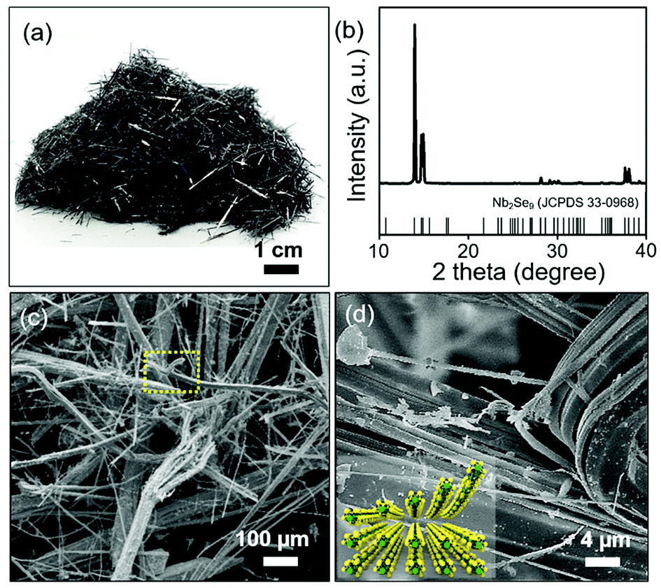 | ||
| Fig. 1 (a) Photograph of the mass-production of needle-like Nb2Se9 crystals; (b) XRD pattern of the Nb2Se9 crystal; (c) and (d) low- and high-magnification SEM images of the Nb2Se9 crystal. The inset shows an illustration of the crystal structure of Nb2Se9. | ||
To examine the characteristics of the layered structure of the Nb2Se9, the bulk Nb2Se9 crystal was cleaved via conventional peeling method.2 It was easily separated into Nb2Se9 flakes adopting a quasi-two-dimensional layered structure and transferred onto a 300 nm SiO2/Si substrate. Fig. 2 shows the SEM and AFM images of the quasi-two-dimensional Nb2Se9 flake with three-layer thicknesses on a 300 nm SiO2/Si substrate.
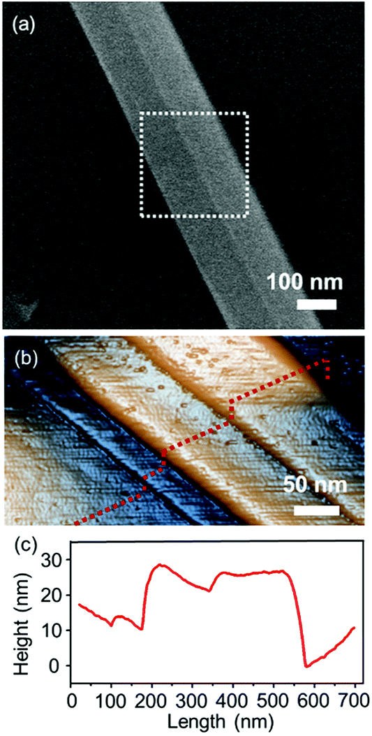 | ||
| Fig. 2 (a) SEM and (b) 3D AFM images of the exfoliated quasi-two-dimensional Nb2Se9 flake on a 300 nm SiO2/Si substrate. (c) Line profile of the corresponding Nb2Se9 flakes, as marked in (b). | ||
Through weak vdW interactions, we were able to control the number of layers of the Nb2Se9 flakes. Fig. 3(a) shows the AFM images of several exfoliated Nb2Se9 flakes with different thickness on a 300 nm SiO2/Si substrate. After the second peeling process at the same position using blue tape, the thickness of flakes reduced from 160 to 107 nm (P1 to P1′), and from 80 to 30 nm (P2 to P2′), as shown in Fig. 3(b) and (c).
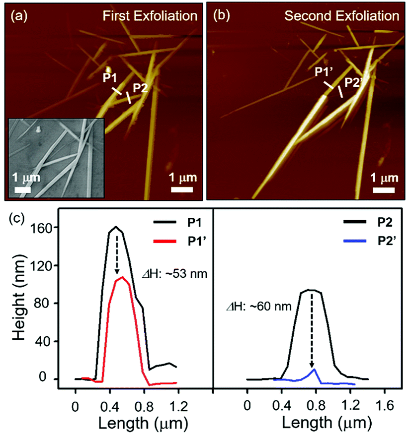 | ||
| Fig. 3 (a) AFM image of the exfoliated quasi-two-dimensional Nb2Se9 flakes on a 300 nm SiO2/Si substrate. (b) AFM image of the exfoliated Nb2Se9 flakes on a 300 nm SiO2/Si substrate after an additional peeling process. (c) Line profile of the Nb2Se9 flakes before and after a second exfoliation. | ||
An isolated monolayer of Nb2Se9 can be obtained on the 300 nm SiO2/Si substrate after multiple peeling processes. Fig. 4 shows the quasi-two-dimensional structure of Nb2Se9 with a single chain thickness and a width of approximately 200 nm (Fig. 3(b)). Because Nb2Se9 is composed of single chains of Nb2Se9 without dangling bonds, it is likely that the exfoliated quasi-two-dimensional Nb2Se9 would exhibit ideal transport characteristics without degradation caused by edge scattering.
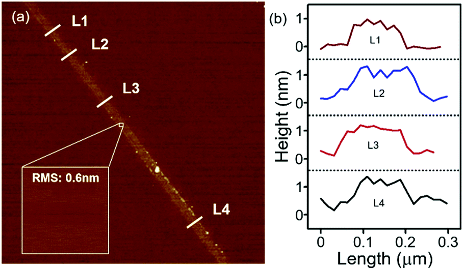 | ||
| Fig. 4 AFM image of exfoliated quasi-two-dimensional monolayer Nb2Se9 on 300 nm SiO2/Si substrate. The inset shows the HR-AFM image of selected regions and its RMS value. (b) Line profile of quasi-two-dimensional monolayer Nb2Se9 ribbon as marked L1, L2, L3, and L4 in (a). | ||
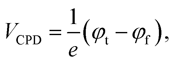
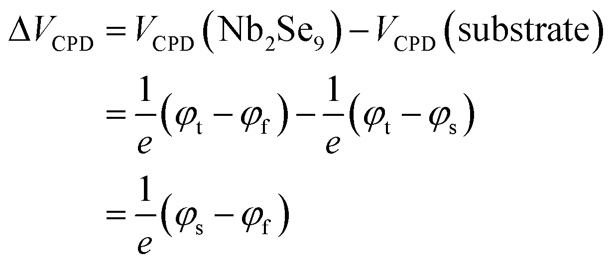
The electrical properties of the Nb2Se9 flakes with different thicknesses were investigated by SKPM analysis. SKPM is a non-destructive analytical tool that can probe the local surface potential energy and work function by measuring the contact potential difference between the tip and sample (VCPD).31,32 Since the Nb2Se9 flakes were adhered onto a Si substrate, the work can be calculated using the following equation:
where φt, φs, and φf represent the contact potential difference and work functions of the tip, Si substrate, and Nb2Se9 flakes, respectively.
As shown in Fig. 5(a), the distribution of the surface potential energy was homogeneous over the entire surface of each flake, but its value varied depending on its thickness. The surface potential energy difference between 5 nm (L1, 5–6 layers) and 20 nm (L2, approximately 20–22 layers) thick Nb2Se9 flakes and the Si substrate were 20 and 40 mV, respectively (Fig. 5(b) and (c)). The statistical results of >28 samples show that both the surface potential energy difference and work function begin to decrease as the thickness of the Nb2Se9 flakes decreases to <20 nm due to interlayer screening effects, which were also observed in typical layered materials (Fig. 5(d) and (e)).31 The surface of the Si substrate was covered by a naturally formed hydrophilic Si oxides, generating large numbers of charge trapping sites. These sites strongly influenced the charge transfer behavior between the Nb2Se9 and Si substrate. Since the effective length of the interlayer screening effects increases with decreasing flake thickness, the potential energy difference and work function decreased compared to that of the bulk Nb2Se9.
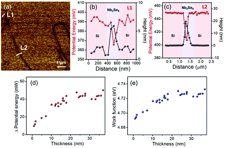 | ||
| Fig. 5 (a) SKPM image of the exfoliated Nb2Se9 flakes on an Si substrate; (b) and (c) height and potential energy profiles of the Nb2Se9 flakes and Si substrate, as marked in (a); (d) and (e) variation of the potential energy difference and work function according to the thickness of the Nb2Se9 flakes. | ||
To evaluate the electrical characteristics of the isolated Nb2Se9 flake, we performed electrical transport measurements of single Nb2Se9 field effect transistor (FET) (Fig. 6). The current–voltage (Ids–Vds) curve at various gate voltage (Vg) and current–gate voltage (Ids–Vg) curve exhibited p-type field effect transistor characteristics (Fig. 6(b) and (c)). The transconductance (gm) and field effect electron mobility (μe) were determined from the Ids–Vg with the drain bias of 4 V in Fig. 6(b) using the following equations: gm = dIds/dVg, at the maximum slope of the Ids–Vg curve in the linear region and μe = gmL2/CoxVds, where L is the gate length and C is the gate capacitance of a Nb2Se9 flake.33 The oxide capacitance (Cox) per unit area (for the 300 nm SiO2/Si substrate, Cox = 0.2301 fF). The extracted gm and μe values for the Nb2Se9 FET are 12.9 pS and 0.0035 cm2 V−1 s−1.
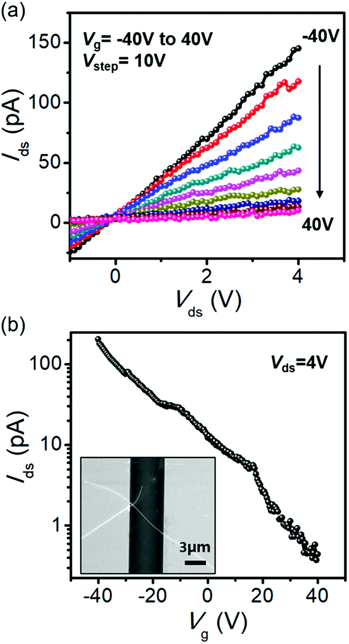 | ||
| Fig. 6 (a) Current–voltage (Ids–Vds) characteristics of the Nb2Se9 FET. (b) Transfer characteristics (Ids–Vg) of the Nb2Se9 FET. Vg = −40 V to 40 V. Inset shows SEM image of the Nb2Se9 FET. | ||
Conclusions
In this study, layered 1D Nb2Se9 was successfully synthesized via niobium–selenium solid-state reaction on a bulk scale. Typical mechanical cleavage afforded a needle-like single crystal Nb2Se9 composed of numerous single Nb2Se9 chains linked by weak vdW interactions. The isolated Nb2Se9 flakes exhibited a quasi-two-dimensional layered structure whose thickness can be controlled by the repeated peeling method. The work function varied as a function of Nb2Se9 flake thickness as determined by SKPM measurements. In particular, the Nb2Se9 FET clearly exhibited p-type semiconductor characteristics with hole mobility of 0.0035 cm2 V−1 s−1. We believe that this novel 1D Nb2Se9 represents an improvement over typical 2D materials and the results of the work function variation may be helpful for selecting a proper metal electrode for future Nb2Se9-based electronic devices.Experimental
Synthesis
Nb2Se9 was synthesized using Nb (99.99%, 325 mesh, Alfa Aesar) and Se (99%, Alfa Aesar) powders. First, 2.15 mmol of Nb and 430 mmol of Se were mixed and pelletized, then sealed in a quartz tube with a neck in the middle. The evacuated quartz tube was heated to 800 °C at 2.3 °C min−1 for 72 h and subsequently cooled. The unreacted Se flux was then removed by dropping the Se flux onto the other side of the tube. The residual Se was sublimed in a tube furnace at 250 °C for 24 h under an Ar atmosphere.Mechanical exfoliation
The bulk Nb2Se9 was placed on wafer dicing tape (BT150EKL, Nitto) and the materials were stuck several times to yield thinner-than-bulk materials. A SiO2/Si substrate was cleaned by ultrasonication in acetone, ethanol, and deionized water for 15 min, followed by heating at 100 °C to remove moisture from the SiO2/Si surface. The polymer tape was strongly pressed against and adhered to and the SiO2/Si substrate. After adhesion, the polymer tape was removed from the SiO2/Si substrate and this process was repeated for exfoliation.Characterization
Powder X-ray diffraction (XRD, Mac Science, M18XHF22) was performed using Cu-Kα radiation (λ = 0.154 nm). Field emission-scanning electron microscopy (FE-SEM, Hitachi, S4300SE) and atomic force microscopy (AFM, Park systems, NX 10) were performed in a non-contact mode for the topographic analysis of the mechanically exfoliated Nb2Se9 on the substrate. SKPM (Park systems, NX10) measurements were performed using Si tips coated by Cr–Pt (Multi75-G, Budget Sensors Inc.) with a resonance frequency of 75 kHz, a scan rate of 0.3 Hz, and a sample bias of ± 1 V.Device fabrication
The Nb2Se9 FET was fabricated by conventional photolithography using p+ Si (100) wafer with a 300 nm thick SiO2 layer on top.33 Metal electrodes were pattered and deposited using thermal evaporator in an ultra-high vacuum (20 nm Cr and 200 nm Au, ∼10−6 Torr). The conducting channel length, width, and the thickness of the Nb2Se9 flake is 5 μm, 400 nm, and 70 nm, respectively (Fig. S2†).Conflicts of interest
There are no conflicts to declare.Acknowledgements
This work was supported by the Technology Innovation Program (or Industrial Strategic Technology Development Program, 10063400, Development of Growth and Transfer Technology for Defectless 350 × 350 mm2 Single Crystalline Graphene) funded By the Ministry of Trade, Industry & Energy (MOTIE, Korea). J. H. Lee acknowledges support from the Presidential Postdoctoral Fellowship Program of the NRF in Korea (2014R1A6A3A04058169).Notes and references
- X. Huang, W. C. Lee, C. Kuo, D. Hisamoto, L. Chang, J. Kedzierski, E. Anderson, H. Takeuchi, Y. K. Choi, K. Asano, V. Subramanian, T. J. King, J. Bokor and C. Hu, IEEE Trans. Electron Devices, 2001, 48, 880–886 CrossRef.
- K. S. Novoselov, A. K. Geim, S. V. Morozov, D. Jiang, M. I. Katsnelson, I. V. Grigorieva, S. V. Dubonos and A. Firsov, Nature, 2005, 438, 197–200 CrossRef CAS PubMed.
- B. Radisavljevic, A. Radenovic, J. Brivio, I. V. Giacometti and A. Kis, Nat. Nanotechnol., 2011, 6, 147–150 CrossRef CAS PubMed.
- A. K. Geim and I. V. Grigorieva, Nature, 2013, 499, 419–425 CrossRef CAS PubMed.
- Y. Zhang, Y.-W. Tan, H. L. Stormer and P. Kim, Nature, 2005, 438, 201–204 CrossRef CAS PubMed.
- C. Lee, X. Wei, J. W. Kysar and J. Hone, Science, 2008, 321, 385–388 CrossRef CAS PubMed.
- Y. W. Son, M. L. Cohen and S. G. Louie, Nature, 2006, 444, 347–349 CrossRef CAS PubMed.
- P. Avouris, Z. Chen and V. Perebeinos, Nat. Nanotechnol., 2007, 2, 605–615 CrossRef CAS PubMed.
- Y. Zhang, T. T. Tang, C. Girit, Z. Hao, M. C. Martin, A. Zettl, M. F. Crommie, Y. R. Shen and F. Wang, Nature, 2009, 459, 820–823 CrossRef CAS PubMed.
- J. Qiao, X. Kong, Z. X. Hu, F. Yang and W. Ji, Nat. Commun., 2014, 5, 4474 CrossRef PubMed.
- A. Castellanos-Gomez, L. Vicarelli, E. Prada, J. O. Island, K. L. Narasimha-Acharya, S. I. Blanter, D. J. Groenendijk, M. Buscema, G. A. Steele, J. V. Alvarez, H. W. Zandbergen, J. J. Palacios and H. S. J. Van Der Zant, 2D Materials, 2014, 1, 025001 CrossRef.
- A. S. Mayorov, R. V. Gorbachev, S. V. Morozov, L. Britnell, R. Jalil, L. A. Ponomarenko, P. Blake, K. S. Novoselov, K. Watanabe, T. Taniguchi and A. K. Geim, Nano Lett., 2011, 11, 2396–2399 CrossRef CAS PubMed.
- F. Schwierz, Nat. Nanotechnol., 2010, 5, 487–496 CrossRef CAS PubMed.
- P. Avouris, M. Freitag and V. Perebeinos, Nat. Photonics, 2008, 2, 341–350 CrossRef CAS.
- J. Wang and M. Musameh, Anal. Chem., 2003, 75, 2075–2079 CrossRef CAS PubMed.
- M. Kusunoki, T. Suzuki, C. Honjo, T. Hirayama and N. Shibata, Chem. Phys. Lett., 2002, 366, 458–462 CrossRef CAS.
- D. N. McCarthy, V. Nicolosi, D. Vengust, D. Mihailovic, G. Compagnini, W. J. Blau and J. N. Coleman, J. Appl. Phys., 2007, 101, 014317 CrossRef.
- J. H. Golden, F. J. DiSalvo, J. M. J. Fréchet, J. Silcox, M. Thomas and J. Elman, Science, 1996, 273, 782–784 CrossRef CAS PubMed.
- B. Messer, J. H. Song, M. Huang, Y. Wu, F. Kim and P. Yang, Adv. Mater., 2000, 12, 1526–1528 CrossRef CAS.
- A. Heidelberg, H. Bloeß, J. W. Schultze, C. J. Booth, E. T. Samulski and J. J. Boland, Z. Phys. Chem., 2003, 217, 573–585 CrossRef CAS.
- F. E. Osterloh, H. Hiramatsu, R. K. Dumas and K. Liu, Langmuir, 2005, 21, 9709–9713 CrossRef CAS PubMed.
- A. Meden, A. Kodre, J. P. Gomilšek, I. Arčon, I. Vilfan, D. Vrbanic, A. Mrzel and D. Mihailovic, Nanotechnology, 2005, 16, 1578–1583 CrossRef CAS.
- N. Sun, M. McMullan, P. Papakonstantinou, H. Gao, X. Zhang, D. Mihailovic and M. Li, Anal. Chem., 2008, 80, 3593–3597 CrossRef CAS PubMed.
- M. I. Ploscaru, S. J. Kokalj, M. Uplaznik, D. Vengust, D. Turk, A. Mrzel and D. Mihailovic, Nano Lett., 2007, 7, 1445–1448 CrossRef CAS PubMed.
- Y. Zhou, L. Wang, S. Chen, S. Qin, X. Liu, J. Chen, D. J. Xue, M. Luo, Y. Cao, Y. Cheng, E. H. Sargent and J. Tang, Nat. Photonics, 2015, 9, 409–415 CrossRef CAS.
- X. Xu, S. Jeong, C. S. Rout, P. Oh, M. Ko, H. Kim, M. G. Kim, R. Cao, H. S. Shin and J. Cho, J. Mater. Chem. A, 2014, 2, 10847–10853 RSC.
- S. Britto, M. Leskes, X. Hua, C. A. Hébert, H. S. Shin, S. Clarke, O. Borkiewicz, K. W. Chapman, R. Seshadri, J. Cho and C. P. Grey, J. Am. Chem. Soc., 2015, 137, 8499–8508 CrossRef CAS PubMed.
- A. Meerschault, L. Guema, R. Berger and J. Rouxel, Acta Crystallogr., Sect. B: Struct. Crystallogr. Cryst. Chem., 1979, 35, 1747–1750 CrossRef.
- S. A. Sunshine and J. A. Ibers, Acta Crystallogr., Sect. C: Cryst. Struct. Commun., 1987, 43, 1019–1022 CrossRef.
- R. Sanjines, H. Berger and F. Levy, Mater. Res. Bull., 1988, 23, 549–553 CrossRef CAS.
- N. J. Lee, J. W. Yoo, Y. J. Choi, C. J. Kang, D. Y. Jeon, D. C. Kim, S. Seo and H. J. Chung, Appl. Phys. Lett., 2009, 95, 222107 CrossRef.
- S. H. Choi, Z. Shaolin and W. Yang, J. Korean Phys. Soc., 2014, 64, 1550–1555 CrossRef CAS.
- J. H. Lee, B.-S. Kim, S.-H. Choi, Y. Jang, S. W. Hwang and D. Whang, Nanoscale, 2013, 5, 8968–8972 RSC.
Footnotes |
| † Electronic supplementary information (ESI) available. See DOI: 10.1039/c8ra07437b |
| ‡ Equal contribution as first author to this work. |
| This journal is © The Royal Society of Chemistry 2018 |