DOI:
10.1039/C8RA06899B
(Paper)
RSC Adv., 2018,
8, 39321-39333
Characterization of electrodeposited undoped and doped thin ZnO passive films on zinc metal in alkaline HCO3−/CO32− buffer solution
Received
17th August 2018
, Accepted 19th November 2018
First published on 26th November 2018
Abstract
Electrochemical characterization of anodically grown thin ZnO films on pure zinc metal was studied in pH 9.2 bicarbonate/carbonate buffer solution. The different undoped passive films were formed potentiostatically in pH 9.2 borate buffer solution at processing anodic voltage (Va) of −1.04, −1.02, −1.0 and −0.99 V (vs. Ag/AgCl). While, various doped ZnO films were fabricated by anodizing the metal at a fixed potential of −1.00 V in the same borate buffer solution containing different amounts of LiCl or InCl3. The electrochemical and semiconducting properties of all formed films were investigated using chronoamperometric measurements, EIS and Mott–Schottky analysis supported by scanning electron microscopy. The impedance results showed a direct correlation between Va and the value of either total resistance (Rf) of undoped passive film or its thickness (δf). It is evident that anodization can afford better conditions for forming thicker compact passive films with more advanced barrier properties. On the other hand, Rf decreases with increasing Li-doping level in the oxide film, and increases in case of In-doping. Interestingly, Rf values of the doped films are always lower when compared to its value for the undoped film grown at −1.00 V, likely due to possible change in the film microstructure upon doping. For both undoped and doped ZnO films, Mott–Schottky plots reveals unintentional n-type conductivity with high electron density. Moreover, with increasing dopant level in ZnO host materials, Mott–Schottky analysis revealed a parallel correlation between charge carrier donor concentration (ND) and the passive film thickness (δf), where the trend of their values are to decrease for Li+-doped and to increase for In3+-doped films.
1. Introduction
Zinc oxide (ZnO) is the most successful semiconductor material in its nanostructure forms due to its wide band gap energy of 3.37 eV and large excitation binding energy of 60 meV which have attracted great interest for several applications in short-wavelength optoelectronic devices and room temperature UV-luminescence.1 Anodization has been investigated for a long time to increase the corrosion resistance by forming protective films on Zn metal.2 The resulting films are widely used in various areas including transparent conductive coatings, electrodes for dye-sensitized solar cells, field emission materials, gas sensing, energy storage, optoelectronic devices, catalysis, UV-lasing action, blue light emitting diodes etc.3,4 It has been shown that anodic oxidation of Zn in alkaline medium can produce ZnO nanowires and porous structures.5,6 Electrodeposition is one of the most common methods for production of metal oxide thin films in the semiconducting process due to its simplicity and ease of implementation, where uniform thin films with various structures and thicknesses can be obtained from zinc oxide. Passive ZnO films formed in various electrolytes have been shown to possess some semiconducting properties which have been found to play an important role on corrosion behavior of zinc in many situations. However, correlations between the electrochemical behavior of zinc oxide and its semiconductive performance are still lacking.7 At low potential, if the forming alkaline medium is at low carbonate concentration, the obtained anodic layers are mainly composed of zincite, (ZnO) and zinc hydroxide.8–12 ZnO formed on zinc surface suggests passivation of zinc in buffer carbonate. Accordingly, passive corrosion traits of ZnO films have to be considered.
It is commonly accepted that structural and electronic properties of ZnO passive layers have a great influence on corrosion performance of zinc and its based alloys in aerated solutions.11 Also, doping which denotes introduction of a small fraction of foreign atoms into a pure intrinsic semiconductor material, is generally used to control the physical, electrical and electronic properties of ZnO materials.13 Wurtzite ZnO is an n-type semiconductor in which the dominant major charge carriers are electrons.14 For an n-type semi-conductor, electrons will be transferred from the electrode into the solution cations. At equilibrium conditions, there is no net transfer of charge, and hence there is no band bending.15 This potential is therefore referred to as the flatband potential (EFB). Among the various dopant impurities in ZnO layers, lithium (Li) is characterized as an acceptor impurity and indium (In) as a donor one.1 Therefore, in the present study Li+ and In3+ ions in solution were incorporated into the transparent conductive oxide ZnO thin films16 during its formation by anodization under potentiostatic conditions to investigate their effect on the electrochemical and semiconducting properties of the resultant films. These two dopants can be used to control the carrier generation which is related to oxygen vacancies. Li and In absorption may lead to different results in crystallization and electrical characteristics, compared to mono-phase oxides.17 It has been shown that increasing dopant concentrations in solution rises and enhances the doping levels in ZnO thin films obtained by electrodeposition and the native n-type semi-conductivity of films.18,19 Other authors have demonstrated that Li doping in ZnO can destine the lattice constant of annealed ZnO![[thin space (1/6-em)]](https://www.rsc.org/images/entities/char_2009.gif) :Li to become slightly larger than that of undoped ZnO because Zn–O bond length (1.97 Å) is slightly smaller than that of Li–O bond (2.01 Å).20 Li-doped ZnO shows the nonstoichiometric point defect.21 Generally, the formation of electrodeposited ZnO can be described by the following equations.4,22,23
:Li to become slightly larger than that of undoped ZnO because Zn–O bond length (1.97 Å) is slightly smaller than that of Li–O bond (2.01 Å).20 Li-doped ZnO shows the nonstoichiometric point defect.21 Generally, the formation of electrodeposited ZnO can be described by the following equations.4,22,23
| | |
Zn → Zn2+ + 2e (anodic reaction)
| (1) |
| | |
2H2O + 1/2O2 + 2e → 2OH− (cathodic reaction)
| (2) |
| | |
Zn2+ + 2OH− → ZnO + H2O
| (3) |
ZnO is mainly described by intrinsic defects, where impurities plays a minor role on its structural, electrical and optical properties.
23
For a semiconductor, the upper, unfilled band is called the conduction band (Ec) while the lower, almost filled band is called the valence band (Ev). The width of the band gap, Eg = Ev − Ec, which is the most important electronic characteristic of a crystal, depends on the strength of chemical bonds. For ZnO, Eg = 3.37 eV at room temperature. Simultaneously, an equal number of positively charged holes are created in the valence band. In an electric field, these holes behave like particles possessing a positive charge equal in absolute value to the charge of the electron. On the other hand, for extrinsic semiconductors, impurities and defects (which have energy levels located in the band gap) are classified as either donors or acceptors. Donors usually located at energy levels slightly below the conduction band give away excess electrons to the conduction band, thereby creating electron conductivity (n-type semiconductors). Acceptors, located at energy levels slightly above the valence band, capture valence electrons from atoms of the basic substance, producing a hole conductivity (p-type semiconductors).
2. Experimental
2.1 Materials and electrochemical methods
Samples were prepared from zinc rod of 99.99% purity as supplied from Johnson and Matthey (England). The samples were abraded with 600 up to 1500 grit emery papers, rinsed with deionized water, dried and then anodically fixed. A borate buffer solution of pH 9.2 (0.05 M H3BO3 + 0.075 M Na2B4O7·10H2O) was used as an electrolyte for preparing the different passive films on pure zinc24 in which ZnO solubility is very low.25,26 These films were formed potentiostatically at controlled potentials over the range from −1.04 V to −0.99 V (vs. Ag/AgCl) for 15 min in order to attain steady state current values.27 Some modifications were made for the passive film formed at −1.0 V by adding Li+ ions or In3+ ions in the concentration ranges 4 × 10⁻⁵ to 8 × 10⁻⁵ M and 6 × 10⁻⁵ to 10 × 10−5 M, respectively, to the borate electrolyte during the anodic treatment. Once the passive film was formed, it was washed with deionized water, dried gently with filter paper and soon immersed in pH 9.2 bicarbonate/carbonate buffer solution for electrochemical characterization. The test medium was composed from 90 ml 0.1 M NaHCO3 + 10 ml 0.1 M Na2CO3 mixture of pH 9.2.28 The anodization was conducted in a typical three-electrode electrolytic cell under constant applied voltage at room temperature of 25 °C. All solutions were prepared using deionized water and analytical grade reagents Applichem panreac, Germany, and their pH values were measured using HANNA 213 pH meter with a combined glass electrode. Electrochemical measurements were performed in the following sequence:
(i) After reaching steady state open circuit potential in the treatment borate solution, anodization was started at the prescribed applied potential value and the associated anodic current was recorded with time every 0.5 min for a period of 15 min which was sufficient to obtain a steady state current value.
(ii) Electrochemical impedance spectroscopy (EIS) was recorded in a fresh pH 9.2 buffer HCO3−/CO32− solution using the electrochemical workstation IM6e Zahner-electrik GmbH, Meβtechnic, Kronach, Germany. The measurements were done in a conventional three-electrode system with anodized zinc electrode as the working electrode, large platinum sheet as the counter electrode and Ag/AgCl (3 M KCl) as the reference electrode. An excitation AC signal with amplitude of 10 mV peak-to-peak was employed over a frequency domain from 50 kHz down to 10 mHz, unless otherwise stated.
(iii) Mott–Schottky experiments were conducted on zinc electrodes bearing the formed passive films at a fixed frequency of 3 kHz using 10 mV sinusoidal AC signal and a step potential from −0.5 to 0.9 V (vs. Ag/AgCl), in the anodic direction. The chosen frequency has to be higher than the characteristic frequencies of reactions linked to redox species present in the solution.29 The flatband potential and charge carrier concentrations were determined from Mott–Schottky analysis for ZnO. The semiconducting properties of an oxide film can be studied by measuring the capacitance of the interface layer developed in the oxide film when the electrode is immersed in an electrolyte as a function of the experimental factor under investigation. The experimental parameters tested in the present work include passive film formation voltage, as well as nature and dopant concentration.
2.2 Surface examination
The morphology of surface films formed at different experimental conditions were observed using field emission scanning electron microscopy (FE-SEM), Quanta 250 FEG (Field Emission Gun), Netherlands.
3. Results and discussion
3.1 Effect of anodizing voltage
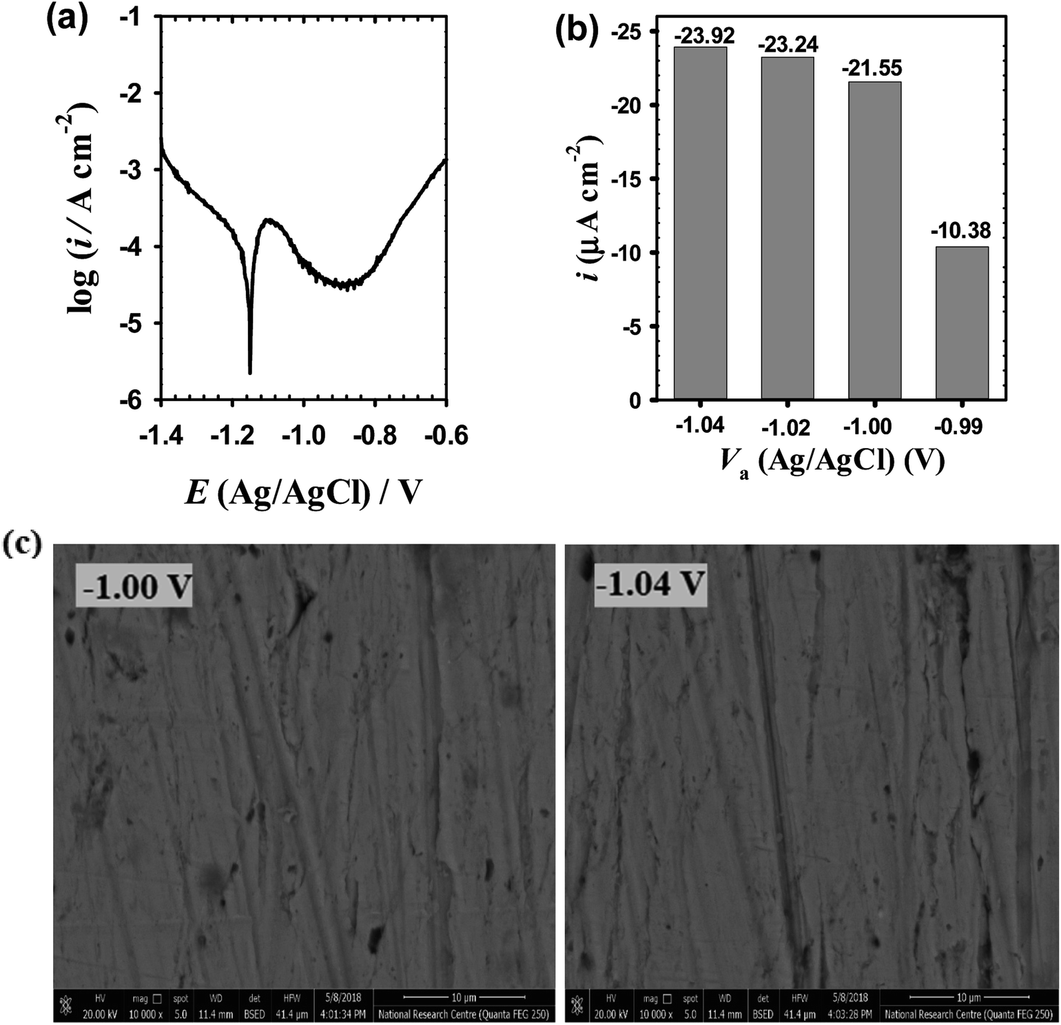
3.1.1 Chronoamperometric behavior. Chronoamperometry is an electrochemical technique by which the potential of the working electrode is stepped and the response current is recorded as a function of time. At each stepped potential, anodization was extended for 15 min to ensure the formation of a thin passive films on the zinc substrate.2 A complete polarization curve was first recorded for bare zinc surface in pH 9.2 borate buffer solution in order to select the anodizing voltage (Va) values to be used for passive ZnO film formation. As can be seen in Fig. 1a the best passive region chosen for forming anodic passive films in the present work is from −1.04 to −0.99 V (vs. Ag/AgCl). This is to avoid oxygen generation at potentials more positive than −0.99 V as observed during anodic polarization scan of zinc in borate buffer solution that accompanied the passive film formation. Fig. 1b shows the chronoamperometric behavior of ZnO after 15 min immersion. At each selected formation voltage the current was found to decrease exponentially with time to a steady value indicating a continuous growth of a protective passive film on the zinc surface which impedes the flow of electronic charge.30 Fig. 1b presents the steady state current density (ia) value measured after 15 min anodization where it is noted that ia decreases with increasing the processing voltage. This trend indicates a monotonic increase in the oxide formation layers with the applied voltage. However, the current efficiency for the oxide formation decreases gradually with increasing the forming potential over the tested domain from −1.04 V to −0.99 V. This behavior most probably is due to changes not only in the film thickness, but also to possible changes in its morphological microstructure as supported by the two FE-SEM images shown in Fig. 1c.
 |
| | Fig. 1 (a) Potentiodynamic polarization curve of pure Zn in pH 9.2 borate buffer solution. (b) Chronoamperometric current values after 15 min potentiostatic anodization of pure Zn at different voltages (Va). (c) FE-SEM micrographs of anodic ZnO thin films formed on zinc substrate at −1.00 and −1.04 V (vs. Ag/AgCl) in pH 9.2 borate buffer solution followed by immersion in pH 9.2 bicarbonate solution for 20 min. | |
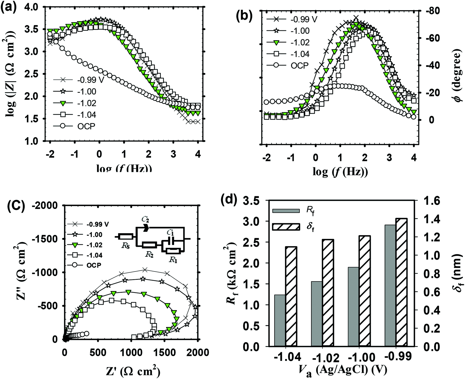
3.1.2 EIS measurements. Electrochemical impedance spectroscopy (EIS) occupies a special important place among various electrochemical methods as being nonionizing and noninvasive technique.31 It is one of the powerful tools for investigating properties of anodic passive films of metals and characterizing their semiconductor behavior. The impedance spectra of anodic ZnO thin passive films on zinc substrate measured in pH 9.2 HCO3−/CO32− buffer solution as a function of their anodizing voltage (Va). EIS measurements were recorded directly after forming the 15 minute thin passive films in pH 9.2 borate buffer solution at different controlled anodic processing voltages of −1.04, −1.02, −1.0 and −0.99 V (vs. Ag/AgCl). Impedance spectra are represented in both logarithm of the impedance modulus (log|Z|) and phase angle (φ) plotted as a function of logf (Bode diagrams in Fig. 2a and b respectively), as well as the imaginary component (Z′′) of the impedance plotted as a function of the real component (Z′) (Nyquist diagrams in Fig. 2c). The results generally reveals a continuous increase in the absolute impedance (|Z|) over middle (MF) to low frequency (LF) region from 10 to 0.1 Hz with increasing Va value (Fig. 2a). This is associated with a parallel increase in the phase angle maximum (φmax) as shown in Fig. 2b, where its value increases from −65.39° at −1.04 V to −71.48° at −0.99 V. At the LF region of 10−1 Hz to 10−2 Hz there is no significant difference between the impedance values of the four tested oxide films. Each plot on the Nyquist format (Fig. 2c) displays a feature of two merged distorted semicircle capacitive loops with an overall size that continuously increases as the forming voltage (Va) is raised from −1.04 until −0.99 V. Such behavior can be attributed to a continuing improvement in the passive performance of the anodic surface film with increasing its processing voltage (Va). The highly similar shapes of Nyquist plots suggest that the Va value only changes the properties of the formed passive film and has no impact on the film formation mechanism. Impedance results of un-anodized bare zinc electrode measured in the same buffer solution are also included in Fig. 2a–c for comparison. The exceptional higher impedance values of anodic films compared to that of spontaneously formed one suggests that anodization can significantly enhances the protective capability of the surface film due to growing of ZnO passive layer with a better barrier properties on the substrate surface, that can be further boosted with increasing Va value.
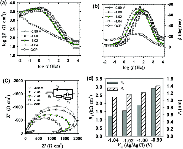 |
| | Fig. 2 Impedance spectra in pH 9.2 bicarbonate buffer solution for ZnO films on pure Zn formed at different anodic voltages (Va vs. Ag/AgCl) in pH 9.2 borate buffer solution: (a and b) Bode diagrams and (c) Nyquist diagrams. (d) Effect of Va on the total film resistance (Rf) and its thickness (δf). | |
In order to evaluate the important impedance parameters necessary to interpret the obtained impedance responses, the experimental EIS data could be analyzed using the proposed equivalent circuits (EC) depicted in Fig. 2c inset. This electronic model was selected based on the high and low frequency features of the impedance Bode and Nyquist diagrams where it was found to be appropriate to accurately fit the measured EIS data and to simulate well the results with an average error of less than 0.4%. The model consists of two parallel time constants in series with the solution resistance (Rs) between the reference and working electrode.32 In this adopted electronic model (Fig. 2c inset) the first time constant parallel combination (R1C1) is linked to the system behavior at the low LF region which comes from the resistance and capacitance effects due to the inner barrier oxide layer. On the other hand, the second time constant is the parallel combination (R2C2) describing the behavior in the MF to HF region of the charge transfer resistance and the capacitance at the outer oxide layer/solution interface.32,33 This explanation is based on the well-established notion that passive film formed on zinc normally is bi-layer structure comprising an inner barrier layer in direct contact to the metal substrate covered by an outermost layer facing the solution.9 In order to modify the suggested EC model due to non-ideal behavior, a constant phase element (CPE) had replaced the pure capacitor (C2) in real electrochemical process. The used CPE is not an ideal capacitor accounting for the non-uniform current distribution caused by roughness and inhomogeneity of the outermost layer. The CPE impedance is defined by the following equation:28,32–34
where
n is a CPE empirical exponent ranging from zero to one (0 ≤
n ≤ 1),
Q is the CPE admittance (Ω
−1 cm
−2 s
n) and
j is the complex unit

. The two factors
Q and
n are both independent of the frequency
f (s
−1) of applied ac signal during the impedance scan. The deviation of
n from unity is an indication of deviation of
Q from ideal capacitance. At frequency
f = 1/2π, the angular frequency
ω = 1, where
ω = 2π
f (rad s
−1), then
Q would be equal to the capacitance
C (F cm
−2).
35 A good agreement between experimental data and simulated ones are noticed for all tested anodic films, which are also imbedded in the impedance plots of
Fig. 2a–c.
Table 1 summarizes the obtained fitted impedance parameters of the used EC model. As can be seen, R1 is of kΩ cm2 order and R2 is of only Ω cm2 order, while C1 is inferior to C2 (at least 30 times less). This behavior clearly indicates that the inner layer of the anodic passive film is more resistive and has much higher insulting properties than its outermost layer. As the processing anodic voltage (Va) is increased the total resistance (Rf = R1 + R2) of the formed oxide film increases, while its total capacitance (Ct = C1 + C2) is decreased. This behavior hints to a decrease in the corrosion susceptibility of the metal substrate owing to an increase in the protective efficacy of the formed passive film with increasing its processing Va value.36,37 Based on the parallel plate capacitor model, the capacitance of the interface is related to the passive film thickness (δf) according to the following relation:28,38,39
where
ε is the dielectric constant of the passive film (8.5 for ZnO),
40 ε0 is the permittivity of the free space (8.854 × 10
−14 F cm
−1) and
A is the geometric surface area of the electrode.
Eqn (5) indicates a reverse correlation between
Ct and
δf which points towards a direct increase in the film thickness (
δf) with increasing the anodizing voltage (
Va) as depicted in
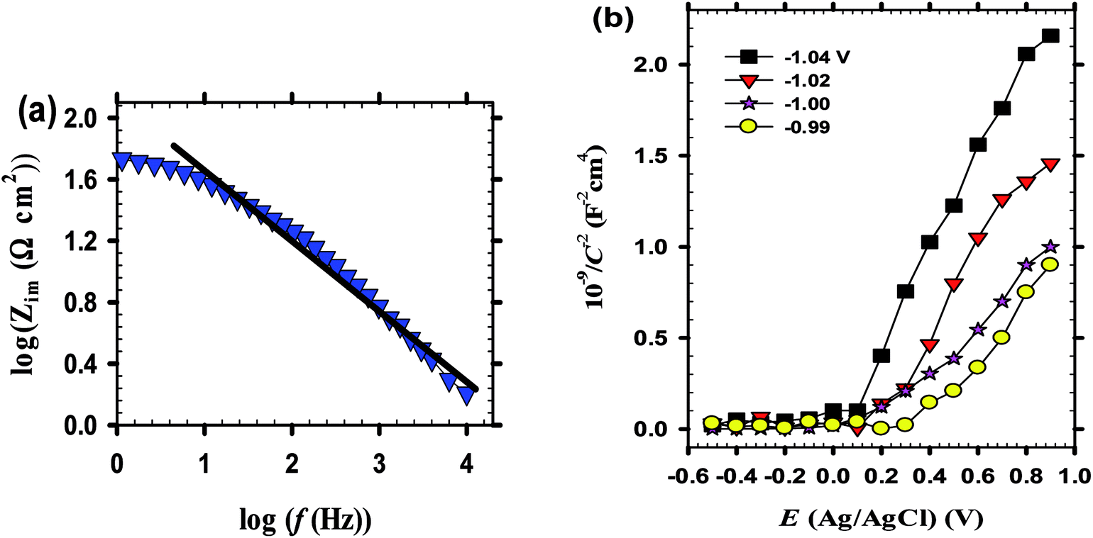
Fig. 2d. Additionally, the linear plot of log
Zim vs. log
f shown in
Fig. 3a, has a constant slope with a value of -
n confirming the presence of an oxide layer on bare zinc substrate in pH 9.2 bicarbonate buffer solution.
41
Table 1 Equivalent circuit parameters of the impedance data in pH 9.2 bicarbonate buffer solution for undoped ZnO film as a function of the forming anodic voltage (Va)
| Va (VAg/AgC) |
R1 (kΩ cm2) |
C1 (μF cm−2) |
R2 (Ω cm2) |
C2 (μF cm−2) |
n |
RS (Ω cm2) |
| −1.04 |
1.23 |
0.23 |
7.96 |
6.62 |
0.860 |
22.9 |
| −1.02 |
1.55 |
0.18 |
8.08 |
6.23 |
0.863 |
17.8 |
| −1.00 |
1.89 |
0.08 |
8.85 |
6.12 |
0.859 |
17.0 |
| −0.99 |
2.90 |
0.06 |
9.10 |
5.29 |
0.856 |
29.6 |
 |
| | Fig. 3 (a) Logarithm of the imaginary part of the impedance (logZimg) for bare zinc substrate in pH 9.2 bicarbonate buffer solution as a function of logf. (b) Mott–Schottky plots in pH 9.2 bicarbonate buffer solution for the formed anodic ZnO films on pure Zn in borate buffer solution as a function of the processing anodic voltages (Va). | |
3.1.3 Semiconducting properties. The electronic properties of the surface oxide film on a substrate is among the critical values determining its electrochemical performance in a given environment. According to the point defect model, the passive film on a pure metal is usually a highly defective semiconductor oxide layer which is best described by Mott–Schottky theory. This defect structure is formed due to a set of defect generation and annihilation reactions occurring at the metal/barrier layer interface and the outer layer/solution interface.42–44 Generally, the point defect present in a barrier oxide layer are cation vacancies  , oxygen vacancies
  and cation interstitials
  . Cation vacancies are electron acceptors resulting in the p-type conduction, whereas oxygen vacancies and/or cation interstitials are electron donor resulting in n-type conduction.45–47
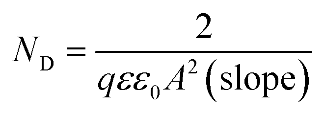
Fig. 3b shows the Mott–Schottky plots for the passive films formed anodically on zinc metal measured in pH 9.2 bicarbonate buffer solution as a function of the processing anodic voltage (Va) over the range −1.04 to −0.99 V. A reasonably linear relationship between C−2 and E with a positive slope observed for all tested films reveal their n-type semiconductor behavior. This implies that conductivity of those passive films mainly relies on oxygen vacancies and zinc cation interstitials which are preponderance over metal vacancies in the barrier layer and creating shallow donor levels just below the conduction band.40,48–52 The evolution of the main charge carrier density as a function of the film anodizing voltage confirms well the impedance results. In fact, for a semiconductor/electrolyte interface its capacitance (C) is related to the space charge capacitance (Csc) and the Helmholtz capacitance (CH), where C−1 = Csc−1 + CH−1. Commonly, Csc ≪ CH and therefore C ≈ Csc. Hence, according to Mott–Schottky theory, the relation between the space charge capacitance and the applied electrode potential (E) can thus be described by eqn (6):53–55
| |
 | (6) |
where
q is the electron elementary charge (1.602 × 10
−19 C),
ND is the charge carrier donor concentration and
EFB is the flat band potential. Based on the Mott–Schottky (MS) analysis of the plots in
Fig. 3b, the slope of the linear MS plot is commonly used to determine the free charge carrier concentration:
. While the intercept of the plot as well as the slope can be both used to calculate the flatband potential:
, where

at room temperature which is a very small quantity and thus can be neglected (
k being the Boltzmann's constant, 1.38 × 10
−23 J K
−1).
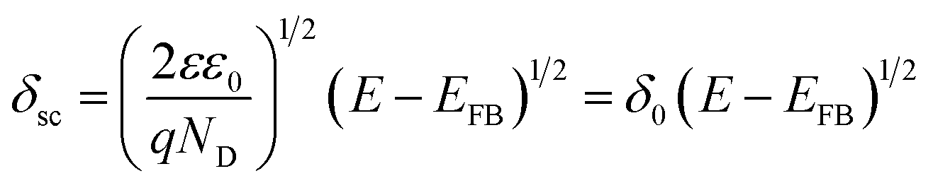
The values of ND and EFB obtained from the linear part of MS plots in Fig. 3b are summarized in Table 2 which includes also δf values. The calculated donor concentrations are relatively higher than the value for the unanodized bare zinc substrate being equal to 1.81 × 1020 cm−3 as obtained in the same pH 9.2 bicarbonate buffer solution.28 The donor density concentration (ND) obviously increases with increasing Va value and subsequently as the film thickness (δf) is increased. On the other hand, the obtained flat band potentials (EFB) are in good agreement with previously relevant values28,36 and becomes more negative with the increase of the processing anodic voltage (Va). The observed results can be generally understood based on the fact that existing donor level arises due to highly disorder nature of the formed passive film and its relation to the width of the depletion layer, i.e. the thickness of space charge region (δsc) through the following expression (eqn (7)):28,53
| |
 | (7) |
Table 2 Mott–Schottky plots data in pH 9.2 bicarbonate buffer solution for the undoped electrodeposited ZnO thin film as a function of the forming anodic voltage (Va)
| Va (VAg/AgC) |
ND (cm−3) |
EFB (V) |
δf (nm) |
| −1.04 |
6.32 × 10²¹ |
−0.031 |
1.09 |
| −1.02 |
8.21 × 10²¹ |
−0.128 |
1.17 |
| −1.00 |
9.79 × 10²¹ |
−0.276 |
1.21 |
| −0.99 |
12.56 × 10²¹ |
−0.280 |
1.40 |
A further simplification can be made by observing that δsc = δfCsc. In this way, calculated values of δsc as a function of Va should give the same trend as the film thickness (δf) with the growth of its processing anodic voltage (Va) (Table 2). It follows that ND of the anodic passive film on zinc substrate is a direct function of its processing voltage (Va), and the shift in its band potential towards more negative values is a consequence of the increase in film formation voltage and the impact it has on rising donor concentration level in the applied bicarbonate buffer solution as an electrolyte.56,57 Taking degeneracy into consideration, high dopant levels are generally not accessible in the bulk oxides. The order of the donor densities in this process are 1021 cm−3 which is analogous with that reported in literature.28,58,59
3.2 Effect of doping by lithium and indium
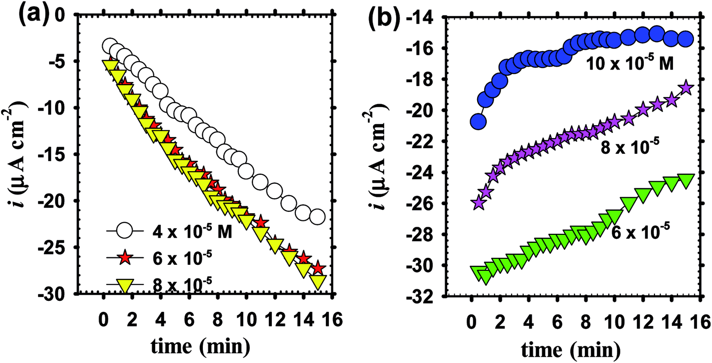
3.2.1 Chronoamperometric behavior. Among the various doping methods, electrodeposition growth in aqueous solution has been an important approach for ZnO deposition with doping capabilities. This is due to variety of advantages such as low-cost, non-vacuum and easy doping.60,61 Dopant nature and concentration are two essential growth parameters worth to be studied, as they can modulate the deposition conditions for doped ZnO materials, and thus modified its electrochemical and electronic characteristics for some useful technical applications.1,62 The dopant acts as a donor when it occupies a substitutional position for Zn2+ cation or an interstitial position in the ZnO lattice. In the current work lithium (Li) and indium (In) are selected as doping candidates, where Li is considered as an acceptor dopant while In is considered as a donor one.1,63,64Before commencement the electrochemical experimentation, chronoamperometric behavior of zinc as a substrate is needed to be measured for 15 min which is the time duration for electrodeposition of doped ZnO passive films in pH 9.2 borate buffer solution containing the dopant cations Li+ or In3+ at various concentrations. At the chosen fixed applied voltage of −1.00 V vs. Ag/AgCl, Fig. 4a displays a non-significant decrease in current density with the increase of Li+ ion level in borate solution loaded with 4 × 10⁻⁵, 6 × 10⁻⁵ and 8 × 10⁻⁵ M LiCl, but it falls rapidly with time.4,51 On the other hand, Fig. 4b reveals that the current density increases with time and significantly with increasing In3+ ion level in solution within the range 6 × 10⁻⁵ to 10 × 10−5 M InCl3.65,66 It should be noticed that the recorded dissolution current densities during In–ZnO deposited films have higher negative values than those for the Li case.67 The results remarkably demonstrate that during potentiostatic anodizing growth, Li can sustain dissolution more than the formation process with time laps. Meanwhile, In can help to shift the formation-dissolution process more towards a net growth development in good agreement with the well-known fact that In content in ZnO thin films decreases the resistivity of the deposited films.68 It is worth to note that, under the same deposition conditions and current efficiency the incorporated amount from Li and In atoms in the crystalline structure of the fabricated doped ZnO would be, in all cases, a direct function of the dopant concentration in the borate buffer processing solution.
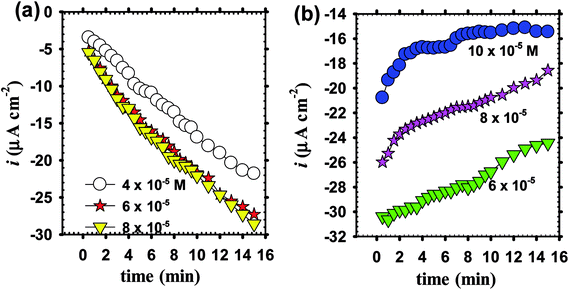 |
| | Fig. 4 Chronoamperometric plots during the formation of doped ZnO films for 15 min in pH 9.2 borate buffer solution at −1.00 V vs. (Ag/AgCl) as a function of the dopant concentration. (a) Li+, and (b) In3+. | |
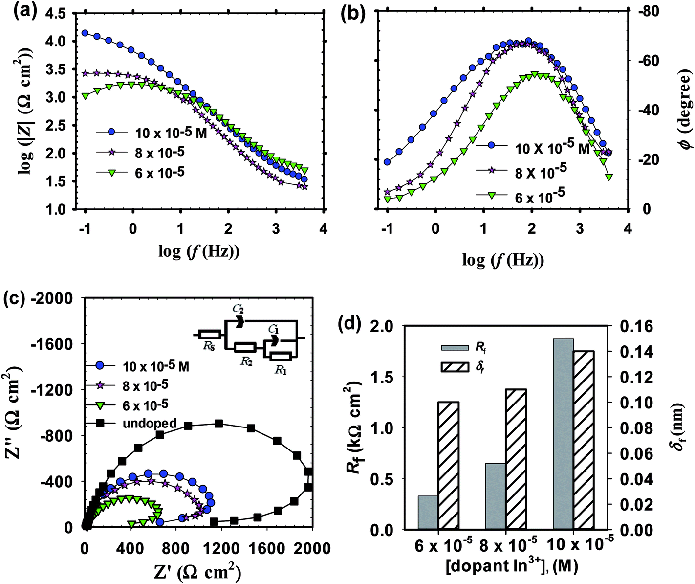
3.2.2 EIS measurements. In order to investigate the influence of Li and In doping on the electrochemical characteristics of the doped anodic passive films on pure zinc metal, EIS measurements were performed in pH 9.2 bicarbonate buffer solution for the resultant six passive films fabricated as described in Section 3.2.1. The impedance spectra traced after 15 min anodization are presented on Bode and Nyquist diagrams as a function of the dopant concentration in Fig. 5a–c for Li doped films and in Fig. 6a–c for In doped ones. The results validate that nature and concentration of the dopant ions have both a substantial influence on the impedance spectra of the undoped passive film, which is also incorporated for comparison in Fig. 5c and 6c. By comparing the size of the capacitive loop, it is evident that undoped passive film exhibits always higher impedance behavior than those for the doped films, albeit having the same shape. Obviously, for lithium doped films the increase of Li+ doping spawns in decreasing the absolute impedance (|Z|) and phase maximum as shown in Fig. 5a and b with a concomitant reduction in the size of the capacitive loops on the Nyquist diagrams (Fig. 5c). Nonetheless, for indium doped films a reverse trend can be realized for the change of impedance spectra and phase with raising In3+ ion doping as observed in Fig. 6a–c. Such behavior indicates relative continuous improvement of passive film on zinc substrate with the increase of indium amount in the doped film. In all cases a broad phase maximum is observed in the Bode ɸ-logf plots at the medium frequencies. At high frequencies, the impedance and phase have both similar shape irrespective of the dopant concentration but a big variation can be seen at the low frequency range (<50 Hz).
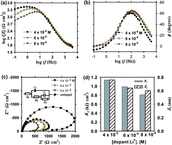 |
| | Fig. 5 Impedance spectra in pH 9.2 bicarbonate buffer solution for the anodized Zn at −1.00 Va as a function of Li+ dopant concentration (a and b) Bode diagrams and (c) Nyquist diagrams. (d) Effect of dopant amount on the total film resistance (Rf) and its thickness (δf). | |
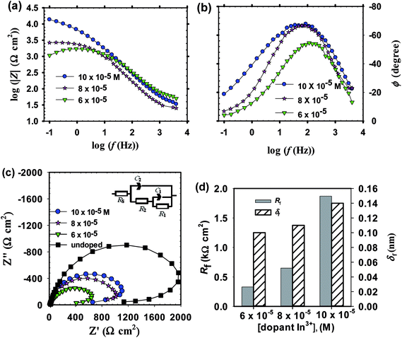 |
| | Fig. 6 Impedance spectra in pH 9.2 bicarbonate buffer solution for the anodized Zn at −1.00 V as a function of In3+ dopant concentration (a and b) Bode plots and (c) Nyquist plots. (d) Effect of dopant amount on the total film resistance (Rf) and its thickness (δf). | |
The obtained EIS spectra for both Li and In doped passive films on zinc substrate measured in pH 9.2 bicarbonate buffer solution can be described by an equivalent circuit model comprised two time constants similar to the one used for the EIS data analysis of undoped anodic ZnO films, as given in Fig. 5c and 6c insets. In the case of In doped films two effective CPE exponent parameters were used24 (Fig. 6c inset) to allow a more accurate analysis for their impedance data. The fitted EC impedance parameters thus obtained are all summarized in Table 3. For both Li and In doped films, upon increasing dopant concentration in solution an inverse relation can be realized between total film resistance (Rf) and capacitance (Cf). Nonetheless, for Li doped films Rf decreases while Cf increases with doping concentration, while a reverse trend can be recognized in the case of In doped films.
Table 3 Equivalent circuit parameters of the impedance data in pH 9.2 bicarbonate buffer solution for doped ZnO films formed on pure Zn at different dopant concentrations (Li+ and In3+)
| Dopant (M) |
R1 (kΩ cm2) |
C1 (μF cm−2) |
n1 |
R2 (kΩ cm2) |
C2 (μF cm−2) |
n2 |
RS (Ω cm2) |
| Li+ |
| 4 × 10⁻⁵ |
0.40 |
3.22 |
— |
0.74 |
6.57 |
0.837 |
20.4 |
| 6 × 10⁻⁵ |
0.35 |
4.20 |
— |
0.64 |
7.53 |
0.839 |
17.3 |
| 8 × 10⁻⁵ |
0.28 |
4.41 |
— |
0.53 |
8.00 |
0.887 |
18.1 |
|
| In3+ |
| 6 × 10⁻⁵ |
0.12 |
54.0 |
0.590 |
0.21 |
18.8 |
0.812 |
6.9 |
| 8 × 10⁻⁵ |
0.25 |
45.4 |
0.568 |
0.40 |
21.4 |
0.850 |
3.4 |
| 10 × 10−5 |
0.97 |
27.7 |
0.765 |
0.90 |
24.4 |
0.825 |
4.2 |
Determination of the thickness (δf) for doped ZnO passive film was also intended using eqn (5) mentioned above. With increasing dopant amount in the processing solution, it is clear from Fig. 6d that for In doped films of thickness (δf) and total resistance (Rf) are both increased,69 yet these two parameters are decreased for the case of Li doping (Fig. 5d). In good corroboration with the present findings, Shinde et al.70 have previously reported that the increase of indium content in solution increases the resistivity of ZnO film for [In]/[Zn] ratio higher than 3 at% due to the deterioration of the (101) preferential growth. On the other hand, for Li doped ZnO thin film Chiu and Wu71 observed a decrease in the grain-boundary resistance from 60 to 2 kΩ with increasing Li content from 0.1 to 0.5 mol%. Fig. 7 shows a quick comparison between FE-SEM micrographs for undoped and doped ZnO thin films formed on zinc substrate at the same anodizing voltage (Va) of −1.00 V and same dopant amount of 6 × 10⁻⁵ M from Li+ or In3+. As can be shown, the undoped film has an intact and compact microstructure in comparison with the doped ones. In the meanwhile, the morphology of In doped film has somewhat more defective feature than that of Li doped one, which is in good support of EIS results.
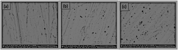 |
| | Fig. 7 FE-SEM micrographs of ZnO thin films formed on zinc substrate at anodizing voltage Va = −1.00 V (vs. Ag/AgCl) (a) undoped ZnO, (b) Li+ doped ZnO, and (c) In3+ doped ZnO at concentration of 6 × 10⁻⁵ M from each dopant in the processing borate buffer solution. | |
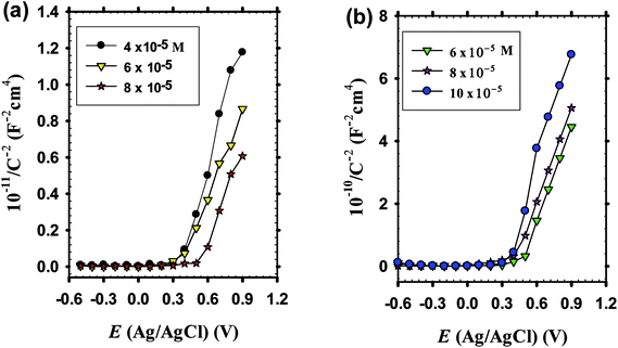
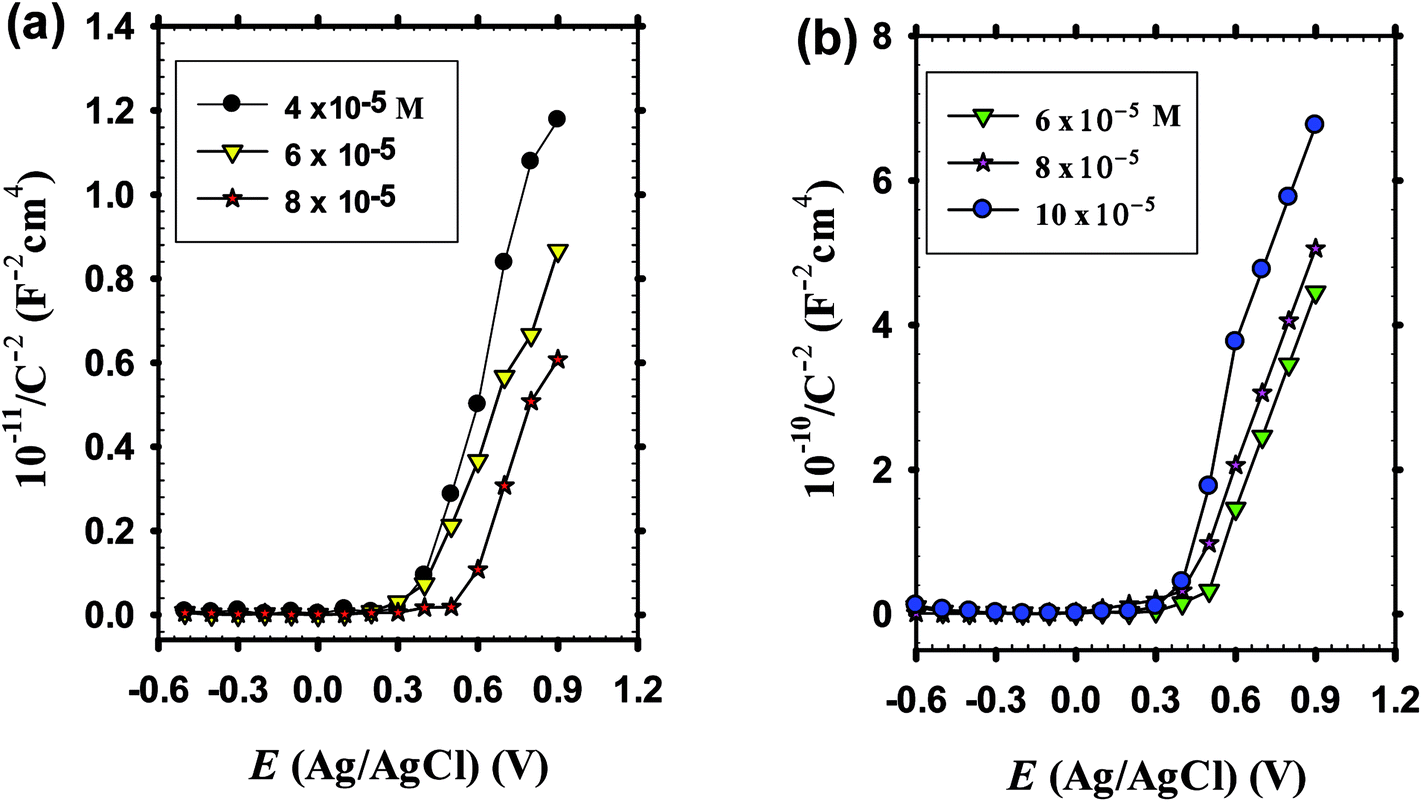
3.2.3 Mott–Schottky analysis. Vacancies, interstitials and antisites of Zn and of O are considered to be the native point defects in ZnO connected with its n-type conductivity.1,72 Zinc interstitials is a shallow donor but it has high formation energy. Oxygen vacancy has low formation energy but it is a deep donor with very high ionization energy that cannot produce high concentration of carrier electrons. The low formation energy of O vacancy makes it responsible for the non-stoichiometry in n-type zinc oxide material (Zn1+δO). Zn antisites are also shallow donors and have even higher formation energies than Zn interstitials. Doping some ions into ZnO material can simply modify and/or control its electrical properties for a wide range of applications. The efficiency of the dopant element is highly related not only to its ionic radius and electronegativity but also to its oxidation states.73 Fig. 8a and b presents the Mott–Schottky plots measured in pH 9.2 bicarbonate buffer solution for doped ZnO films as a function of the dopant concentration Li+ and In3+, respectively. As it can be seen, the dopant nature and its concentration have both significant effect on the electronic properties of the anodic ZnO passive film grown at −1.00 V (vs. Ag/AgCl) for 15 min in the borate buffer solution loaded with dopant ion at different levels. Over the potential range of around 0.45–0.90 V (vs. Ag/AgCl) a reasonably linear relationship with positive slope is observed between C−2 and E. This suggests that conductivity of all doped passive films formed on zinc substrate behave like the undoped ones which mainly relies on n-type semiconducting character. According to eqn (6) charge carrier concentration (ND) and flat band potential (EFB) can be estimated from the slope and intercept of the experimental MS plots and listed in Table 4, which includes also the film thickness (δf) as obtained from EIS results outlined in Section 3.2.2. It can be seen that, increase of Li+ dopant concentration from 4 × 10⁻⁵ M to 6 × 10⁻⁵ M in solution decreases ND value from 1.33 × 1020 cm−3 to almost half its value (6.64 × 1019 cm−3) and continues to decrease a little when Li+ ion is further increased to 8 × 10⁻⁵ M. As for In doped ZnO films a reverse trend can be noted, whereby the increase of In3+ dopant concentration from 6 × 10⁻⁵ M to 10 × 10−5 M leads ND value to increase from 1.60 × 1020 cm−3 to 1.81 × 1020 cm−3. In such two cases, the decreasing and increasing trends in ND value mirrors completely the trend of the film thickness (δf) as shown in Table 4. Furthermore, the shift of flat band potential (EFb) towards less negative value with the increase of Li+ doping is likely considered as a consequence of the decrease in its charger carrier donor concentration (ND). While the reverse is obtained for the indium doped films as EFb is found to continuously move in the more negative direction with the increase of In3+ doping coincidentally with the increase in its ND value.67,70 A comparison between the three types of ZnO passive films studied in the present work is illustrated schematically in Fig. 9.
 |
| | Fig. 8 Mott–Schottky plots in pH 9.2 bicarbonate buffer solution of doped ZnO films on pure Zn as a function of dopant concentration (a) Li+ (b) In3+. | |
Table 4 Mott–Schottky plots data in pH 9.2 bicarbonate buffer solution for doped ZnO films formed on pure Zn at different dopant concentrations (Li+ and In3+)
| Dopant (M) |
ND (cm−3) |
EFB (V) |
δf (nm) |
| Li+ |
| 4 × 10⁻⁵ |
1.33 × 10²⁰ |
−1.10 |
0.769 |
| 6 × 10⁻⁵ |
6.64 × 10¹⁹ |
−0.70 |
0.642 |
| 8 × 10⁻⁵ |
6.58 × 10¹⁹ |
−0.39 |
0.606 |
|
| In3+ |
| 6 × 10⁻⁵ |
1.60 × 10²⁰ |
−0.45 |
0.103 |
| 8 × 10⁻⁵ |
1.71 × 10²⁰ |
−0.51 |
0.113 |
| 10 × 10−5 |
1.81 × 10²⁰ |
−0.60 |
0.144 |
 |
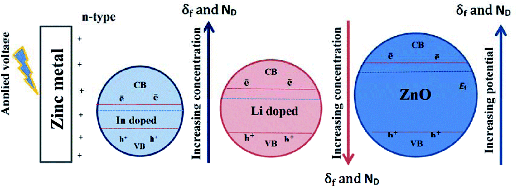
| | Fig. 9 Schematic illustration for the trend of charge carrier density (ND) and anodic film thickness (δf) dependence on the parameter indicated on each arrow for undoped, Li-doped, and In-doped ZnO semiconductor materials. | |
It is well established that, depending on its relative size doping can induce crystal distortion of the host ZnO lattice causing an increase of its internal energy and hence a major decrease of its stability (Rt decrease).73 The doped In3+ ion with larger radius (80 pm) tends to occupy the grain boundaries of expansion lattice and doped Li+ ion with smaller radius (76 pm) trend to occupy the grain boundaries of compression lattice. This means that concentration of doped ion at the grain boundary is higher than that in the bulk. At the grain boundary these enriched ions can form a diffusion barrier, which would suppress the growth of ZnO crystal when compared to the undoped film, being of higher Rt value than Li or In doped films. Additionally, electronegativity can verify rational doping effect of Li and In. thus, Li element has lower electronegativity value (0.98) compared with that of Zn (1.65) and the presence of Li atom for the interstitial cation site is thus due to the ease by which it loses its valence electron.20 On the other hand, indium has larger ionic radius (80 pm) than Zn (74 pm) with a somehow higher electronegativity (1.78–2.2) and presence of In3+ cation in a substitutional position for Zn2+ cation would expand the host lattice with increasing In doping amount (Fig. 10). More recently, Yu et al.74 found that with increasing In doping concentration in the synthesized indium doped n-ZnO nanorods, the average diameter increased and the number of nanorods per area decreased. At the same time, the incorporation of In also affects the optical properties of ZnO nanorods, whereby among others, the intensity of visible emission peak increased due to the increase of oxygen vacancies  by In doping. Such results confirm well our present findings which reveals that upon increasing In doping level in the host n-ZnO film both of δf and ND values increase and EFb shifts towards more negative potential values (Table 4, Fig. 10).
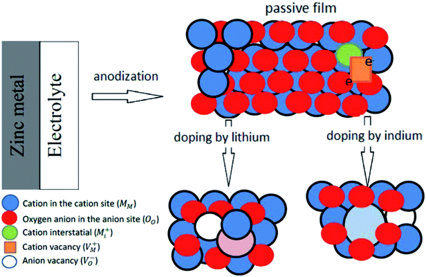 |
| | Fig. 10 Schematic representation for undoped and doped electrodeposited ZnO films. | |
4. Conclusions
Herein, we report the electrochemical and semiconducting properties of electrodeposited undoped and doped ZnO thin passive films on pure Zn metal as investigated in pH 9.2 bicarbonate/carbonate buffer solution. The undoped films were processed in pH 9.2 borate buffer solution at controlled anodic voltages (Va) of −1.04, −1.02, −1.00 and −0.99 V (vs. Ag/AgCl), whereas the doped films were fabricated at −1.00 V as a function of the dopant amount (Li+ or In3+ ions) in the same borate buffer solution. The following are the main conclusions which can be drawn from the obtained results.
(1) Anodization can significantly enhances passive film formation on Zn substrate with higher barrier capability. For undoped passive films grown within the potential range from −1.04 V to −0.99 V (vs. Ag/AgCl), the anodic dissolution current density decreases continuously with increasing the processing anodic voltage due to the growth of ZnO passive film on the surface. Comparing the chronoamperometric curves for the doped films, it is noticeable that Li+ ions can sustain the dissolution more than the formation process with time laps. Meanwhile, In3+ ions can help to shift the formation-dissolution process more towards a net growth process, as the dissolution current density decreases during In–ZnO deposited films and increases for the Li–ZnO case.
(2) EIS results showed that the total resistance (Rf) of undoped ZnO passive film and its thickness (δf) are both increased by increasing the processing anodic voltage (Va). These two parameters are found to decrease significantly for the Li or In doped films when compared to their corresponding values for the undoped film grown at −1.00 V. Noting that, with the increase of dopant concentration the general trends for Rf and δf values are boths to decrease for Li-doped films and to increase for the In-doped case.
(3) Mott–Schottky plots reveal unintentional n-type conductivity with high electron density for both undoped and doped ZnO passive films. Mott–Schottky analysis showed also that with increasing Va value the increase in charger carrier donor concentration (ND) of undoped ZnO films matches well the increase in film thickness as obtained from the impedance results.
(4) Upon increasing each dopant level in ZnO host materials, the analysis revealed a direct correlation between the charge carrier donor concentration (ND) and passive film thickness (δf). Additionally, the shift in the flat band potential (EFb) towards more negative values with the increase of either Va value or In3+ doping amount is likely considered as a consequence of the increase in charge carrier donor concentration, while the reverse would be true for the Li+ doping case.
Conflicts of interest
There are no conflicts of interest to declare.
Acknowledgements
The authors would like to thank their institutions Faculty of Science, Cairo University and Faculty of Women for Arts, Science and Education, Ain Shams University for all facilities provided.
References
- A. Janotti and C. G. Van de Walle, Rep. Prog. Phys., 2009, 72, 126501 CrossRef.
- M. Dezfoolian, F. Rashchi and R. K. Nekouei, Surf. Coat. Technol., 2015, 275, 245–251 CrossRef CAS.
- N. R. Yogamalar and A. Chandra Bose, Appl. Phys. A, 2011, 103, 33–42 CrossRef CAS.
- G. Jiangfeng, D. Zhaoming, D. Qingping, X. Yuan and Z. Weihua, J. Nanomater., 2010, 2010, 71 Search PubMed.
- J. Park, K. Kim and J. Choi, Curr. Appl. Phys., 2013, 13, 1370–1375 CrossRef.
- S.-S. Chang, S. O. Yoon, H. J. Park and A. Sakai, Appl. Surf. Sci., 2000, 158, 330–334 CrossRef CAS.
- X. G. Zhang, in Corrosion and Electrochemistry of Zinc, Springer, 1996, pp. 93–124 Search PubMed.
- E. Rocca, D. Veys-Renaux and K. Guessoum, J. Electroanal. Chem., 2015, 754, 125–132 CrossRef CAS.
- S. Thomas, I. Cole, M. Sridhar and N. Birbilis, Electrochim. Acta, 2013, 97, 192–201 CrossRef CAS.
- I. Arise, Y. Fukunaka and F. McLarnon, J. Electrochem. Soc., 2006, 153, A69–A74 CrossRef CAS.
- M. Pech-Canul, R. Ramanauskas and L. Maldonado, Electrochim. Acta, 1997, 42, 255–260 CrossRef CAS.
- P. L. Cabot, M. Cortes, F. Centellas, J. Garrido and E. Perez, J. Electroanal. Chem., 1986, 201, 85–100 CrossRef CAS.
- H. Q. Ta, L. Zhao, D. Pohl, J. Pang, B. Trzebicka, B. Rellinghaus, D. Pribat, T. Gemming, Z. Liu and A. Bachmatiuk, Crystals, 2016, 6, 100 CrossRef.
- A. W. Bott, Curr. Sep., 1998, 17, 87–92 CAS.
- A. W. Bott, Curr. Sep., 1998, 17, 87–92 CAS.
- J. Pang, Y. Cai, Q. He, H. Wang, W. Jiang, J. He, T. Yu, W. Liu, Y. Zhang and Y. Sun, Phys. Procedia, 2012, 32, 372–378 CrossRef CAS.
- S.-Y. Han, M.-C. Nguyen, A. H. T. Nguyen, J.-W. Choi, J.-Y. Kim and R. Choi, Thin Solid Films, 2017, 641, 19–23 CrossRef CAS.
- M. A. Thomas and J. Cui, Handbook of Nanoelectrochemistry: Electrochemical Synthesis Methods, Properties, and Characterization Techniques, 2016, pp. 647–679 Search PubMed.
- G. Machado, D. N. Guerra, D. Leinen, J. R. Ramos-Barrado, R. E. Marotti and E. A. Dalchiele, Thin Solid Films, 2005, 490, 124–131 CrossRef CAS.
- J. Lee, S. Cha, J. Kim, H. Nam, S. Lee, W. Ko, K. L. Wang, J. Park and J. Hong, Adv. Mater., 2011, 23, 4183–4187 CrossRef CAS PubMed.
- L. H. Peng, Y. C. Zhang and Y. C. Lin, Appl. Phys. Lett., 2001, 78, 4–6 CrossRef CAS.
- R. Inguanta, C. Garlisi, T. Spano, S. Piazza and C. Sunseri, J. Appl. Electrochem., 2013, 43, 199–208 CrossRef CAS.
- R. Tena-Zaera, J. Elias, C. Lévy-Clément, C. Bekeny, T. Voss, I. Mora-Seró and J. Bisquert, J. Phys. Chem. C, 2008, 112, 16318–16323 CrossRef CAS.
- Z. Feng, X. Cheng, C. Dong, L. Xu and X. Li, Corros. Sci., 2010, 52, 3646–3653 CrossRef CAS.
- I. Milošev, Corros. Sci., 2007, 49, 637–653 CrossRef.
- T. K. Mikić, I. Milošev and B. Pihlar, J. Appl. Electrochem., 2005, 35, 975–984 CrossRef.
- K. K. Naik, R. Khare, D. Chakravarty, M. A. More, R. Thapa, D. J. Late and C. S. Rout, Appl. Phys. Lett., 2014, 105, 233101 CrossRef.
- F. El-Taib Heakal, W. Abd-Ellatif, N. Tantawy and A. Taha, RSC Adv., 2018, 8, 3816–3827 RSC.
- G. Béranger, F. Dabosi and G. Baroux, Corrosion Localisée, EDP Sciences, Paris, 1994 Search PubMed.
- G. Kahanda and M. Tomkiewicz, J. Electrochem. Soc., 1989, 136, 1497–1502 CrossRef CAS.
- A. Lasia, in Modern aspects of electrochemistry, Springer, 2002, pp. 143–248 Search PubMed.
- A. M. Awad, O. S. Shehata and F. E.-T. Heakal, Appl. Surf. Sci., 2015, 359, 939–947 CrossRef CAS.
- F. Mansfeld and M. Kendig, J. Electrochem. Soc., 1988, 135, 828–833 CrossRef CAS.
- M. E. Orazem, I. Frateur, B. Tribollet, V. Vivier, S. Marcelin, N. Pébère, A. L. Bunge, E. A. White, D. P. Riemer and M. Musiani, J. Electrochem. Soc., 2013, 160, C215–C225 CrossRef CAS.
- F. El-Taib Heakal, N. Tantawy and O. Shehata, Corros. Sci., 2012, 64, 153–163 CrossRef CAS.
- X. G. Zhang, Corrosion and electrochemistry of zinc, Springer Science & Business Media, 2013 Search PubMed.
- P. Caswell, N. Hampson and D. Larkin, J. Electroanal. Chem. Interfacial Electrochem., 1969, 20, 335–338 CrossRef CAS.
- B.-Y. Chang and S.-M. Park, Annu. Rev. Anal. Chem., 2010, 3, 207–229 CrossRef CAS PubMed.
- V. A. Alves, L. A. da Silva, L. F. d. F. Santos, D. T. Cestarolli, A. Rossi and L. M. da Silva, J. Appl. Electrochem., 2007, 37, 961–969 CrossRef CAS.
- D. D. Macdonald, K. M. Ismail and E. Sikora, J. Electrochem. Soc., 1998, 145, 3141–3149 CrossRef CAS.
- F. El-Taib Heakal, O. Shehata and N. Tantawy, Int. J. Electrochem. Sci., 2017, 12, 9378–9397 CrossRef CAS.
- D. D. Macdonald, Russ. J. Electrochem., 2012, 48, 235–258 CrossRef CAS.
- D. D. Macdonald, Electrochim. Acta, 2011, 56, 1761–1772 CrossRef CAS.
- D. Macdonald and G. Englehardt, ECS Trans., 2010, 28, 123–144 CAS.
- M. Setvín, M. Wagner, M. Schmid, G. S. Parkinson and U. Diebold, Chem. Soc. Rev., 2017, 46, 1772–1784 RSC.
- M. Mickan, Deposition of Al-doped ZnO films by high power impulse magnetron sputtering, Doctoral thesis, Linköping University Electronic Press, 2017 Search PubMed.
- L. Liu, Z. Mei, A. Tang, A. Azarov, A. Kuznetsov, Q.-K. Xue and X. Du, Phys. Rev. B, 2016, 93, 235305 CrossRef.
- L. Wang, X. Gu, Y. Zhao, Y. Qiang, C. Huang and J. Song, Vacuum, 2018, 148, 201–205 CrossRef CAS.
- C. Supatutkul, S. Pramchu, A. P. Jareonjittichai and Y. Laosiritaworn, Ceram. Int., 2017, 43, S525–S528 CrossRef CAS.
- C. Yilmaz and U. Unal, Appl. Surf. Sci., 2016, 368, 456–463 CrossRef CAS.
- L. Atourki, H. Kirou, A. Elfanaoui, A. Ihlal and K. Bouabid, Materials Today: Proceedings, 2016, 3, 2550–2555 CrossRef.
- A. Fattah-alhosseini and M. S. Joni, J. Alloys Compd., 2015, 646, 685–691 CrossRef CAS.
- H. Jang and H. Kwon, J. Solid State Electrochem., 2015, 19, 3427–3438 CrossRef CAS.
- A. Busic, M. Sagl and G. Fafilek, ECS Trans., 2009, 16, 17–22 CAS.
- K. Gelderman, L. Lee and S. Donne, J. Chem. Educ., 2007, 84, 685 CrossRef CAS.
- J. D. Sloppy, Anodization Mechanism and Properties of Bi-Layer Tantalum Oxide formed in Phosphoric Acid, PhD thesis, The Pennsylvania State University, USA, 2009 Search PubMed.
- E.-J. Lee and S.-I. Pyun, J. Appl. Electrochem., 1992, 22, 156–160 CrossRef CAS.
- Y. K. Frodason, 2016.
- X. Gu, L. Zhu, L. Cao, Z. Ye, H. He and P. K. Chu, Mater. Sci. Semicond. Process., 2011, 14, 48–51 CrossRef CAS.
- G. Machado, D. Guerra, D. Leinen, J. Ramos-Barrado, R. Marotti and E. Dalchiele, Thin Solid Films, 2005, 490, 124–131 CrossRef CAS.
- S. C. Lyu, Y. Zhang, C. J. Lee, H. Ruh and H. J. Lee, Chem. Mater., 2003, 15, 3294–3299 CrossRef CAS.
- M. Skompska and K. Zarębska, Electrochim. Acta, 2014, 127, 467–488 CrossRef CAS.
- S. Ilican, Y. Caglar, M. Caglar and B. Demirci, J. Optoelectron. Adv. Mater., 2008, 10, 2592–2598 CAS.
- D. Zwingel, J. Lumin., 1972, 5, 385–405 CrossRef CAS.
- H. S. Kim, P. D. Byrne, A. Facchetti and T. J. Marks, J. Am. Chem. Soc., 2008, 130, 12580–12581 CrossRef CAS PubMed.
- C. Wu, C. Wu, J. Sturm and A. Kahn, Appl. Phys. Lett., 1997, 70, 1348–1350 CrossRef CAS.
- F. Modine, R. Wheeler, Y. Shim and J. F. Cordaro, J. Appl. Phys., 1989, 66, 5608–5612 CrossRef CAS.
- I. Shih and C. Qiu, J. Appl. Phys., 1985, 58, 2400–2401 CrossRef CAS.
- P. R. Kumar, C. S. Kartha, K. Vijayakumar, T. Abe, Y. Kashiwaba, F. Singh and D. Avasthi, Semicond. Sci. Technol., 2004, 20, 120 CrossRef.
- S. Shinde, P. Shinde, C. Bhosale and K. Rajpure, J. Phys. D: Appl. Phys., 2008, 41, 105109 CrossRef.
- K. C. Chiu and Y. H. Wu, 2012.
- Y.-S. Kim and C. Park, Phys. Rev. Lett., 2009, 102, 086403 CrossRef PubMed.
- X. Yu-Jing, G. Zi-Sheng and H. Tao, Chin. Phys. B, 2014, 23, 087701 CrossRef.
- C. Yu, R. Li, T. Li, H. Dong, W. Jia and B. Xu, Superlattices and Microstructures, 2018 Search PubMed.
|
| This journal is © The Royal Society of Chemistry 2018 |
Click here to see how this site uses Cookies. View our privacy policy here. 
 Open Access Article
 This Open Access Article is licensed under a Creative Commons Attribution-Non Commercial 3.0 Unported Licence
 *a,
W. R. Abd-Ellatifb,
N. S. Tantawyb and
A. A. Tahab
*a,
W. R. Abd-Ellatifb,
N. S. Tantawyb and
A. A. Tahab
 . The two factors Q and n are both independent of the frequency f (s−1) of applied ac signal during the impedance scan. The deviation of n from unity is an indication of deviation of Q from ideal capacitance. At frequency f = 1/2π, the angular frequency ω = 1, where ω = 2πf (rad s−1), then Q would be equal to the capacitance C (F cm−2).35 A good agreement between experimental data and simulated ones are noticed for all tested anodic films, which are also imbedded in the impedance plots of Fig. 2a–c.
 , oxygen vacancies
  and cation interstitials
  . Cation vacancies are electron acceptors resulting in the p-type conduction, whereas oxygen vacancies and/or cation interstitials are electron donor resulting in n-type conduction.45–47
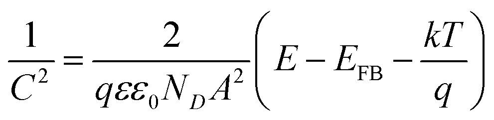
 . While the intercept of the plot as well as the slope can be both used to calculate the flatband potential:
 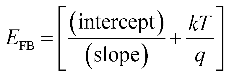 , where
 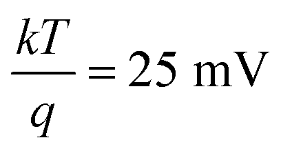 at room temperature which is a very small quantity and thus can be neglected (k being the Boltzmann's constant, 1.38 × 10⁻²³ J K−1).


 by In doping. Such results confirm well our present findings which reveals that upon increasing In doping level in the host n-ZnO film both of δf and ND values increase and EFb shifts towards more negative potential values (Table 4, Fig. 10).