DOI:
10.1039/C8RA06692B
(Paper)
RSC Adv., 2018,
8, 34817-34822
Effects of annealing temperature on properties of InSnZnO thin film transistors prepared by Co-sputtering
Received
9th August 2018
, Accepted 26th September 2018
First published on 10th October 2018
Abstract
Indium-tin-zinc-oxide (ITZO) as the channel layer grown by co-sputtering of ZnO target and ITO target in the bottom gate thin-film transistors (TFTs) is proposed in this work. The microstructure and optical properties of ITZO thin films at different annealing temperatures were analyzed. The impact of various annealing temperatures on the ITZO TFT performance characteristics was systematically investigated as well. It was found that ITZO TFT with annealing temperature of 300 °C exhibits excellent electrical performance with a high saturation field-effect mobility (μsat) of 27.4 cm2 V−1 s−1, a low threshold voltage (Vth) of −0.64 V, a small subthreshold swing (SS) value of 0.23 V per decade, and the high on-off current ratio (Ion/Ioff) of 1.8 × 10⁷. In addition, it also shows good output curves including gate control capabilities and good electrode contact as well as extreme atmospheric stability. As shown by photoluminescence (PL) analysis and X-ray photoelectron spectroscopy (XPS) analysis, the beneficial effects of various annealing temperatures on device performance are attributed to the reorganization of the amorphous network and the control of defect chemistry in the films. The correlation between the post-deposition thermal treatment and the characteristics of a transistor was investigated and excellent performance of the transistor was demonstrated.
1. Introduction
Zinc oxide-based compound semiconductors are different from conventional polycrystalline zinc oxide as they exhibit amorphous state by physical vapor deposition (PVD).1,2 An advantageous feature of the ZnO-based compound semiconductor is that the metal cation composition of the high quality film can be easily controlled by a co-sputtering process.3 ZnO-based compound semiconductors are promising materials for making the channel layer of thin-film transistor (TFT) in the next generation display backplanes because they can accomplish high mobility and large-area uniformity at low temperature process.4 As a representative material of ZnO-based compound semiconductors, a-IGZO has been widely studied since Hosono et al. first used amorphous indium gallium zinc oxide (a-IGZO) as the channel layer of TFT.3–5
However, for next-generation displays requiring ultra-high-definition and high-frame-rate, mobility of ∼10 cm2 V−1 s−1 observed in IGZO TFTs is not enough to drive the backplanes. Therefore, a ZnO-based TFT with high mobility is indispensable. Since Grover et al. reported the amorphous indium zinc tin oxide (a-IZTO) with good field effect mobility in the range of ∼15 cm2 V−1 s−1, it has attracted the attention as a possible alternative to amorphous InGaZnO (a-IGZO).6,7 Just as Ga atom can be used as a carrier generation inhibitor to suppress the formation of oxygen-related defects in IGZO thin films, Sn atom can also be used to suppress the formation of oxygen-related defects in amorphous ITZO thin films.8 Besides, the bottom of the ITZO conduction band is mainly composed of In 5s and Sn 5s orbitals, which have strong divergence and high symmetry, thereby improving carrier mobility and reducing carrier recombination. In addition to the role of the Sn atom, the annealing temperature is another important factor affecting the presence of defects in the material. Since oxygen vacancies in oxide semiconductors are the main source of free electrons, the conductivity of the film can be altered by controlling the oxygen vacancy content in the film during annealing, thereby affecting the device performance.9–11 In this paper, the microstructure and optical properties of ITZO thin films at different annealing temperatures were analyzed, and the effects of different annealing temperatures on the performance of ITZO TFTs were investigated. In addition, the impact of different annealing temperatures has been applied to develop high electrical characteristics and extremely stable ITZO TFTs.
2. Experimental
A schematic diagram of the manufactured bottom-gate ITZO TFT is shown in Fig. 1. A 300 nm-thicklayer of Al–Nd alloy (3wt% of Nd) was deposited on a glass substrate by direct current sputtering and patterned by wet etching as a gate electrode. Then, it was anodized to form a 200 nm-thick layer of AlOx![[thin space (1/6-em)]](https://www.rsc.org/images/entities/char_2009.gif) :Nd on the surface as the gate dielectric layer.12 After that, a 60 nm-thick ITZO thin film was deposited on the AlOx:Nd thin film with the Ar/O2 flow rate of 9/6 sccm by a co-sputtering method of ZnO target (99.99%, CHINO New Material Technology Co., Ltd) and ITO target (90 wt% In2O3 and 10 wt% SnO2, 99.99%, CHINO New Material Technology Co., Ltd). During the deposition process, the deposition power of the ITO target was set to be 70 W DC, and the deposition power of the ZnO target was set to be 130 W RF. The composition of the ITZO film was studied using X-ray photoelectron spectroscopy (XPS) technology. The quantities of In, Sn, and Zn occupied among metal cations were found to be 40.05%, 2.97% and 56.98%, respectively. For the source electrode and the drain electrode, a 240 nm-thick ITO layer was applied through the stencil mask printing, and a channel width/length of 300 μm/300 μm was defined. Finally, the devices were annealed in air at different temperatures (250 °C, 300 °C, 350 °C, and 400 °C) for 90 min.
:Nd on the surface as the gate dielectric layer.12 After that, a 60 nm-thick ITZO thin film was deposited on the AlOx:Nd thin film with the Ar/O2 flow rate of 9/6 sccm by a co-sputtering method of ZnO target (99.99%, CHINO New Material Technology Co., Ltd) and ITO target (90 wt% In2O3 and 10 wt% SnO2, 99.99%, CHINO New Material Technology Co., Ltd). During the deposition process, the deposition power of the ITO target was set to be 70 W DC, and the deposition power of the ZnO target was set to be 130 W RF. The composition of the ITZO film was studied using X-ray photoelectron spectroscopy (XPS) technology. The quantities of In, Sn, and Zn occupied among metal cations were found to be 40.05%, 2.97% and 56.98%, respectively. For the source electrode and the drain electrode, a 240 nm-thick ITO layer was applied through the stencil mask printing, and a channel width/length of 300 μm/300 μm was defined. Finally, the devices were annealed in air at different temperatures (250 °C, 300 °C, 350 °C, and 400 °C) for 90 min.
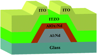 |
| | Fig. 1 Schematic diagram of the sputtered ITZO thin film transistor. | |
X-ray diffraction (XRD) measurements were conducted on a PANalytical X′Pert PRO X-ray diffractometer with Cu Kα radiation. The surface morphology of the films were characterized using atomic force microscopy (AFM) (Bruker, MultiMode8). The transmittance spectra of the films were obtained using a Shimadzu 2550 PC spectrophotometer. Photo-luminescence (PL) spectra were recorded at room temperature by exciting the samples with a Xe lamp at an excitation wavelength of 325 nm on a Hitachi-F4500 luminescence spectrometer. In order to characterize the chemistry of oxygen vacancies in ITZO films prepared at different annealing temperatures, X-ray photoelectron spectroscopy (XPS) measurement was performed on the Physical Electronics 5600 multi-technique system. For accurate detection, 5 nm thick film surfaces were etched with Ar ions prior to XPS characterization. The electrical measurements of the TFTs were performed in air using a semiconductor parameter analyser (Agilent 4155C).
3. Results and discussion
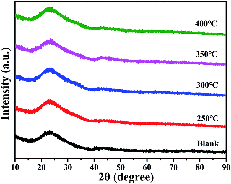
The XRD patterns of 60 nm-thick ITZO films with different annealing temperatures (250 °C, 300 °C, 350 °C, and 400 °C) and a blank quartz glass are shown in Fig. 2. The experimental results in Fig. 2 indicate that only halo peaks in the XRD patterns can be attributed to the glass substrate, which means that the ITZO films have an amorphous structure and are independent of the annealing temperature. This result is consistent with the previous studies.13,14 The amorphous phase of the ITZO thin film is attributed to the reorganization of the amorphous network between the hexagonal ZnO growth reaction and ITO growth reaction during the reactive sputtering process.
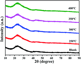 |
| | Fig. 2 XRD patterns of ITZO thin-films deposited on glass substrates with different annealing temperatures (250 °C, 300 °C, 350 °C, and 400 °C) and a blank glass substrate. | |
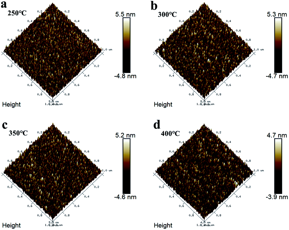
To better understand the ITZO film microstructure, AFM images depicting the surface morphology of the film were taken and are shown in Fig. 3. No significant grain and grain boundaries were observed in all samples. This is consistent with the XRD results in Fig. 2. As shown in Fig. 3, the root-mean-square (RMS) roughness of the ITZO films treated at 250 °C, 300 °C, 350 °C, and 400 °C were 1.49 nm, 1.44 nm, 1.44 nm, and 1.24 nm, respectively. The smooth surface shows good interface characteristics, and could effectively inhibit the formation of interface charge traps and reduce the carrier scattering center, thus achieving a high field-effect mobility and significantly improving the performance of TFTs.15
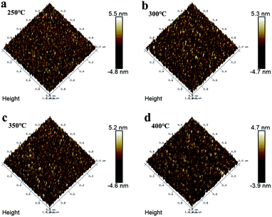 |
| | Fig. 3 AFM images of the surface of ITZO films annealed at different temperatures (250 °C, 300 °C, 350 °C, and 400 °C). | |
The study of optical transmission characteristics is very important in the next generation of flexible transparent electronic applications. Fig. 4 shows the optical transmittance of the ITZO film annealed at different temperatures on glass substrate. As shown in the figure, the optical transmittance of the ITZO film is in the range of 83.6–98.9% in the visible light range (400–800 nm). As the annealing temperature increases from 250 °C to 400 °C, the average transmittance decreases from 89.3% to 87.8%, indicating that the annealing temperature affects the optical band gap of the film. The optical energy band gap (Eg, eV) of ITZO films was estimated from the inset in Fig. 4, which is determined as the crossing point between the line extrapolated from the linear part of the hν versus (αhν)2 curve and x-axis of the plot according to Tauc equation.16 As can be seen from the inset figure, as the annealing temperature increases from 250 °C to 400 °C, the Eg of the thin film decreases from 3.44 eV to 3.23 eV. The possible mechanism is that thermal annealing is an effective method for curing the randomness of deposited atoms in deposited films, which can increase the degree of atom ordering.17 It may be because the increase in annealing temperature increases the long-range ordering of unit cells, resulting in more and more Sn atoms and In atoms directly overlapping in the Sn 5s orbital and In 5s orbital space.
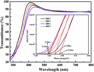 |
| | Fig. 4 Optical properties of ITZO films deposited at room temperature onto glass substrates at various annealing temperatures in the range of 250–400 °C. Inset: the plot of (αhν)2 as a function of hν. | |
The room-temperature PL spectra of the ITZO films annealed at different temperatures (250 °C, 300 °C, 350 °C and 400 °C) obtained with an excitation wavelength of 325 nm are shown in Fig. 5(a) and (b). These films exhibit an asymmetric and broad PL spectrum from the ultraviolet to the visible region. The asymmetric and broad peaks of the ITZO film annealed at different temperatures were fitted well with four Gaussian curves using pick multiple peaks from a curve to fit pure Gaussian function. The Gaussian fit shows four symmetrical peaks centered at 386 nm, 414 nm, 437 nm, and 446 nm (Fig. 5(a)). As shown in Fig. 5(a), the first peak near 386 nm (3.2 eV) may be related to bound excitons.18–20 Some researchers suggested that it is attributed to the UV emission of the radiative recombination of excitons near conduction band levels at the exciton level.21,22 The second peak in the visible range of 413 nm (3.0 eV) is attributed to transitions from the Sni level to VBM.20 The third peak at about 437 nm (2.84 eV) can be attributed to the transition from Sni to VSn and from the zinc gap (Zni) to the zinc vacancy (VZn).23–25 The fourth emission peak of the dominant PL spectrum at about 446 nm (2.78 eV) is attributed to oxygen vacancy-related defects, which results in two donor levels below the conduction band minimum of 1.3–1.6 eV and 0.3–0.5 eV.26 The energy gap from the top of the valence band to the shallow donor level is approximately 2.8 eV, which is in good agreement with the 2.78 eV light photon energy observed in our experiment. Therefore, the fourth emission at about 446 nm (2.78 eV) is due to the electron transition from the shallow donor level band of the oxygen vacancy to the top of the valence band.27–30
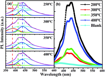 |
| | Fig. 5 (a) Gaussian fitting is illustrated using the spectrum of ITZO film treated at different temperatures (250 °C, 300 °C, 350 °C, and 400 °C). (b) PL spectra of ITZO films annealed in air for 90 min at different temperatures and a blank glass substrate. | |
It is worth noting that, ITZO thin film annealed at 300 °C shows that less intense emission peaks correspond to 384, 414, 437, and 446 nm than the thin film annealed at 250 °C (Fig. 5(b)). When the ITZO thin films were annealed in oxygen, many oxygen atoms were absorbed into the film and occupied oxygen vacancies in the film. Oxygen vacancies in the film decreased and the film became more stoichiometric, which lead to a decrease in the PL intensity. However, the PL intensity began to increase as the annealing temperature was increased to 350 °C. This is because ITZO thin films also tend to lose oxygen and become non-stoichiometric at high temperatures, which often occurs in ZnO thin films.26 When the ITZO thin films were annealed at high temperatures, the films became more non-stoichiometric due to the desorption of oxygen at high temperature, and the oxygen vacancies and zinc/tin interstitials density increased significantly, which lead to a significant increase in PL intensity. Therefore, the PL spectrum in Fig. 5(b) clearly shows that the ITZO thin film annealed at 300 °C has the least density of defects such as oxygen vacancies, tin vacancies/interstitials, and zinc vacancies/interstitials.
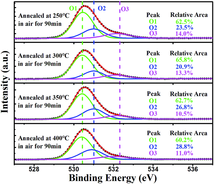
To further investigate the effect of annealing on the chemical composition of ITZO thin films, XPS characterization was used to analyze the chemical states of oxygen in ITZO thin films annealed at various temperatures. Fig. 6 depicts XPS O 1s spectra with fitting curves (O1, O2, and O3 sub-peaks) by a 20% Lorentzian–Gaussian ratio fit and the relatively area ratio of O1, O2, and O3 peaks obtained from ITZO films thermally annealed at different temperatures. The O 1s spectra of all samples were found to be well separated into three Gauss–Lorentz components centered at 530.2 ± 0.1 eV (O1), 531.0 ± 0.2 eV (O2) and 532.2 ± 0.1 eV (O3). The O1 peak is attributed to the oxygen bonded in lattices, such as Zn–O, In–O, and so on.31,32 The O2 peak is related to oxygen ions in the anoxic region of the matrix. Therefore, the change in intensity of this component may be related to the change in oxygen vacancy concentration (VO).32 The O3 peak is attributed to the presence of chemically adsorbed oxygen elements such as adsorbed O2, H2O, and CO2.33 Compared with the 250 °C ITZO film annealing, annealing at 300 °C for 90 minutes results in a 2.6% reduction in the relative percentage of O2, which may be attributed to the reduction of oxygen vacancies in the ITZO film due to thermal oxidation. However, when the annealing temperature exceeds 350 °C, the relative area of the O2 peak increases again. This is because the weak bond strength of Zn–O, In–O, and O can be easily diffused out from ITZO film through a defect-assisted kick-out mechanism at high temperatures, which is often seen in IZO TFTs.34 Oxygen vacancies in ITZO film act as shallow donors,35 and reduction of oxygen vacancies will result in a decrease in carrier concentration in the ITZO film, which is beneficial to build an enhanced TFT with low off-state current.
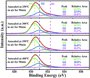 |
| | Fig. 6 XPS O 1s spectra with fitted curves (O1, O2, and O3 sub-peaks) and the relatively area ratio of O1, O2, and O3 peaks obtained from the ITZO thin-films annealed at various temperatures (250 °C, 300 °C, 350 °C, and 400 °C). | |
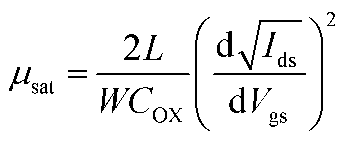
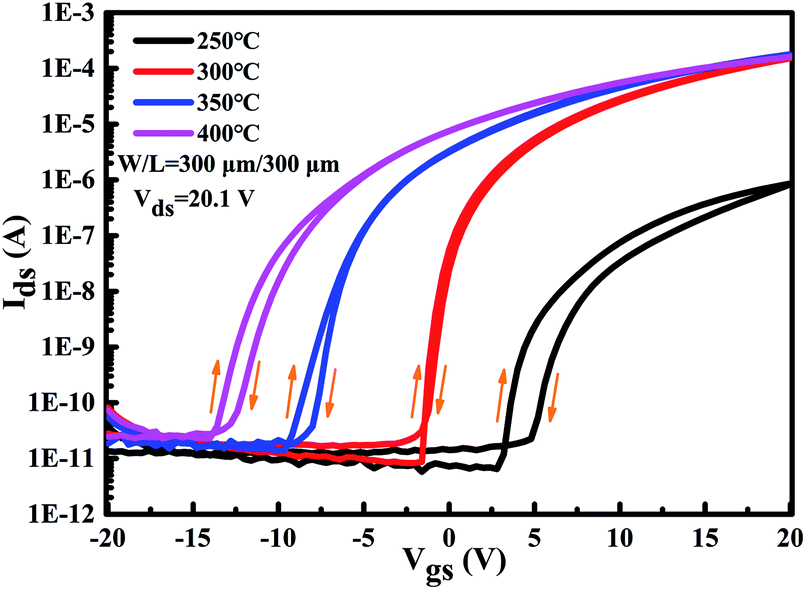
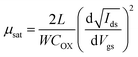
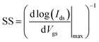
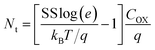
The corresponding transfer characteristics of the ITZO TFTs with different annealing temperatures are shown in Fig. 7. Table 1 summarizes the detailed performance of the ITZO TFTs with different annealing temperatures. In this case, the threshold voltage (Vth) is defined as the corresponding gate voltage (Vgs) when the drain current (Ids) reaches W/L × 10 nA, and W and L are channel width and length, respectively. The saturation mobility was extracted by transfer characteristics with high Vds and subthreshold swing is defined as the inverse of the maximum slope of the transfer characteristic:36
| |
 | (1) |
| |
 | (2) |
where the
COX is the gate capacitance per unit area, the capacitance density of AlO
x:
Nd is 38 nF cm
−2. It is known that SS is related to the density of trap in the bulk of the semiconductor or at the semiconductor/gate insulator interface.
37 The total equivalent trap states can be calculated by using the following equation:
16| |
 | (3) |
where the
kB,
T, and
q are the Boltzmann constant, absolute temperature, and the charge of the electron. It can be observed that as the annealing temperature increases from 250 °C to 300 °C, the electrical characteristics significantly improve and the total trap density reduces to as low as 6.7 × 10
11. According to the results of PL and XPS, although the amount of oxygen vacancies in the process is reduced because Sn restricts the formation of oxygen-related defects in the ITZO film, the direct overlap of Sn 5s orbital and In 5s orbital space leads to higher conduction band electron mobility.
38,39 However, as the annealing temperature continues to increase, the threshold voltage shifts to the negative direction, and the subthreshold swing and the hysteresis also deteriorate. This might be due to the weak bond strength of Zn–O and In–O, so that O can be easily diffused out through a defect-assisted kick-out mechanism and molecular bonds can recombine during annealing process. This phenomenon is common in IZO TFT.
34 Therefore, it is reasonable to infer that the ITZO TFTs with the annealing temperatures of 300 °C exhibits the best electrical performance.with a
μsat of 27.4 cm
2 V
−1 s
−1, a
Vth of −0.64 V, a subthreshold slope (SS) of 0.23 V per decade, and a
Ion/
Ioff of 1.83 × 10
7, which is attributed to the least oxygen-vacancy defects and the lowest carrier concentration benefit from a reasonable annealing temperature. This is consistent with the PL results in
Fig. 5 and the XPS results in
Fig. 6.
 |
| | Fig. 7 The transfer characteristics of the fabricated ITZO TFTs with respect to various annealing temperatures (at 250 °C, 300 °C, 350 °C, and 400 °C). | |
Table 1 Comparison of ITZO TFT electrical parameters with different annealing temperatures
| |
Vth (V) |
μsat (cm2 V−1 s−1) |
Ion/Ioff |
SS (V dec−1) |
Nt (cm−2) |
| 250 °C |
6.53 |
0.3 |
1.48 × 10⁵ |
0.44 |
1.5 × 10¹² |
| 300 °C |
−0.64 |
27.4 |
1.83 × 10⁷ |
0.23 |
6.7 × 10¹¹ |
| 350 °C |
−6.74 |
22.8 |
1.29 × 10⁷ |
0.52 |
1.8 × 10¹² |
| 400 °C |
−11.29 |
15.4 |
7.16 × 10⁶ |
0.76 |
2.8 × 10¹² |
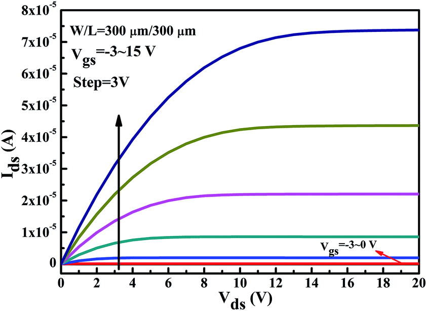
The output curves (Vgs = −3 ∼ 15 V in steps of 3 V) obtained from the ITZO TFT with an annealing temperature of 300 °C is shown in Fig. 8. The output curves show the typical behaviour of an n-channel enhancement TFT. In general, the enhancement mode is more ideal than the depletion mode because the normally-off enhancement transistor consumes less power. It also shows a clear pinch-off and the saturation of Ids at high Vds, reflecting that the gate and drain can effectively control the transistor channel. Besides, no significant current crowding phenomenon is observed in the low drain voltage (Vds) region, indicating an ohmic contact between the ITO electrode and the ITZO channel.
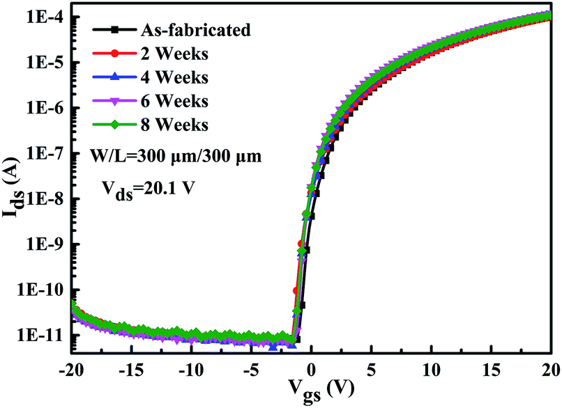
In addition to the remarkable electrical properties, the ITZO TFTs with annealing temperature of 300 °C also exhibit extreme stability in ambient atmosphere. Fig. 9 shows that without any passivation, even after 8 weeks, the ITZO TFT can operate normally with only a small Vth fluctuation while the average Vth shift is only 0.5 V. In addition, no stretching was observed in the sub-threshold region of the transmission curve, and the SS extraction value remained at approximately 0.3 V per decade. This means that only few defects are created within the device during this period. Compared to the case of a-IGZO and polycrystalline ZnO TFTs that have been significantly deteriorated over a long period of time,40,41 the TFTs in our study show extreme atmospheric stability. A possible explanation is that most of the originally exposed ZnO-based back surface is passivated with ITO dielectric material, making it less sensitive to water and oxygen adsorption/desorption processes.42 Therefore, the environmental interaction is well suppressed so that the in situ passivation can be achieved.
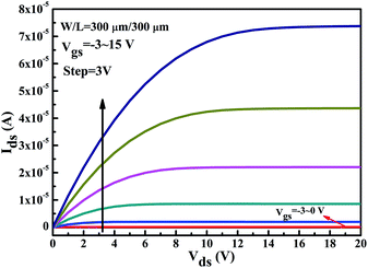 |
| | Fig. 8 The Output curves of ITZO TFT annealed at 300 °C in air for 90 min. | |
 |
| | Fig. 9 The evolution of the transfer curves for the ITZO TFTs with annealing temperature of 300 °C without any passivation in air for 8 weeks. | |
4. Conclusions
In summary, the ITZO thin film was deposited by a co-sputtering technique at room temperature as a channel layer in the TFT. The co-sputtered ITZO film has an amorphous phase structure and the average transmittance exceeds 87% in the visible light range. The results show the ITZO has great potential for the next generation of flexible transparent electronic applications. By adjusting the annealing temperature, the formation of oxygen vacancy defects is effectively controlled, which is confirmed by PL and XPS measurements, making it possible to fabricate ITZO TFTs with high electrical properties. The ITZO TFTs with an annealing temperature of 300 °C were found to exhibit relatively high electrical properties, especially with a high μsat of 27.4 cm2 V−1 s−1, a low Vth of −0.64 V, a small subthreshold swing of 0.23 V dec−1, and excellent air stability. These are attributed to the fact that Sn atom can limit the formation of oxygen-related defects in ITZO films, as the 300 °C annealing temperature allows the device to have the least oxygen-vacancy defects and the lowest carrier concentration. These results indicate that the control of intrinsic defects in ITZO thin films is very important for improving the electrical properties of ITZO TFTs, and the PL and XPS characterization techniques are very useful tools for this purpose.
Conflicts of interest
There are no conflicts to declare.
Acknowledgements
This study was supported in part by the National Natural Science Foundation of China under Grant 61604057, in part by the National Key Technologies Research and Development Program under Grant 2016YFB0401303, in part by the Science and Technology Program of Guangdong Province under Grant 2017A010101010, 2015B090901048, and 2017B090901068, in part by the Science and Technology of Guangzhou under Grant No. 201807010098, in part by the Fundamental Research Funds for the Central Universities under Grant No. 2018MS12, and in part by the opening fund of Key Laboratory of Silicon Device Technology, Chinese Academy of Sciences under Grant No. KLSDTJJ2018-0X.
References
- P. F. Carcia, R. S. Mclean, M. H. Reilly and G. N. Jr, Appl. Phys. Lett., 2003, 82, 1117 CrossRef CAS.
- F. M. Hossain, J. Nishii, S. Takagi, A. Ohtomo, T. Fukumura, H. Fujioka, H. Ohno, H. Koinuma and M. Kawasaki, J. Appl. Phys., 2003, 94, 7768 CrossRef CAS.
- H. Kumomi, K. Nomura, T. Kamiya and H. Hosono, Thin Solid Films, 2008, 516, 1516 CrossRef CAS.
- T. Kamiya, K. Nomura and H. Hosono, Sci. Technol. Adv. Mater., 2010, 11, 44305 CrossRef PubMed.
- K. Nomura, H. Ohta, A. Takagi, T. Kamiya, M. Hirano and H. Hosono, Nature, 2004, 432, 488 CrossRef CAS PubMed.
- M. S. Grover, P. A. Hersh, H. Q. Chiang, E. S. Kettenring, J. F. Wager and D. A. Keszler, J. Phys. D: Appl. Phys., 2007, 40, 1335 CrossRef CAS.
- Y. Goh, J. Ahn, J. R. Lee, W. P. Wan, S. H. K. Park and S. Jeon, ACS Appl. Mater. Interfaces, 2017, 9, 36962 CrossRef CAS PubMed.
- H. K. Noh, K. J. Chang, B. Ryu and W. J. Lee, Phys. Rev. B: Condens. Matter Mater. Phys., 2011, 84, 115205 CrossRef.
- S. Hwang, H. L. Ju, H. W. Chang, J. Y. Lee and H. K. Cho, Thin Solid Films, 2011, 519, 5146 CrossRef CAS.
- S. Y. Sung, K. M. Jo, S. Y. Kim, J. H. Lee, J. J. Kim and Y. W. Heo, J. Nanoelectron. Optoelectron., 2011, 6, 310 CrossRef CAS.
- S. Park, S. Bang, S. Lee, J. Park, Y. Ko and H. Jeon, J. Nanosci. Nanotechnol., 2011, 11, 6029 CrossRef CAS PubMed.
- L. Lan, M. Zhao, N. Xiong, P. Xiao, W. Shi, M. Xu and J. Peng, IEEE Electron Device Lett., 2012, 33, 827 CAS.
- P. Carreras, A. Antony, R. Roldán, O. Nos, P. A. Frigeri, J. M. Asensi and J. Bertomeu, Phys. Status Solidi C, 2010, 7, 953 CAS.
- T. Minami, T. Yamamoto, Y. Toda and T. Miyata, Thin Solid Films, 2000, 373, 189 CrossRef CAS.
- B. Y. Oh, M. C. Jeong, M. H. Ham and J. M. Myoung, Semicond. Sci. Technol., 2007, 22, 608 CrossRef CAS.
- S. Deng, R. Chen, G. Li, Z. Xia, M. Zhang, W. Zhou, M. Wong and H. Kwok, Appl. Phys. Lett., 2016, 109, 182105 CrossRef.
- S. Dai, T. Wang, R. Li, Q. Wang, Y. Ma, L. Tian, J. Su, Y. Wang, D. Zhou, X. Zhang and Y. Wang, J. Alloys Compd., 2018, 745, 256 CrossRef CAS.
- W. I. Park, Y. H. Jun, S. W. Jung and G. C. Yi, Appl. Phys. Lett., 2003, 82, 964 CrossRef CAS.
- D. C. Reynolds, D. C. Look, B. Jogai, C. W. Litton, T. C. Collins, W. Harsch and G. Cantwell, Phys. Rev. B: Condens. Matter Mater. Phys., 1998, 57, 12155 CrossRef.
- N. A. Ahmed, H. Hammache, M. Eyraud, C. Chassigneux, P. Knauth, A. Lahreche, L. Makhloufi and N. Gabouze, Ionics, 2018, 24, 277 CrossRef.
- K. K. Kim, N. Koguchi, Y. W. Ok, T. Y. Seong and S. J. Park, Appl. Phys. Lett., 2004, 84, 3810 CrossRef CAS.
- Y. Yan, Y. Zhang, G. Meng and L. Zhang, J. Cryst. Growth, 2006, 294, 184 CrossRef CAS.
- F. Kayaci, S. Vempati, I. Donmez, N. Biyikli and T. Uyar, Nanoscale, 2014, 6, 10224 RSC.
- P. M. R. Kumar, C. S. Kartha, K. P. Vijayakumar, F. Singh and D. K. Avasthi, Mater. Sci. Eng., B, 2005, 117, 307 CrossRef.
- D. M. Priyadarshini, R. Mannam, M. S. R. Rao and N. Dasgupta, Appl. Surf. Sci., 2017, 418, 414 CrossRef.
- D. H. Zhang, Z. Y. Xue and Q. P. Wang, J. Phys. D: Appl. Phys., 2002, 35, 2837 CrossRef CAS.
- Z. Y. Xue, D. H. Zhang, Q. P. Wang and J. H. Wang, Appl. Surf. Sci., 2002, 195, 126 CrossRef CAS.
- Q. P. Wang, D. H. Zhang, H. L. Ma, X. H. Zhang and X. J. Zhang, Appl. Surf. Sci., 2003, 220, 12 CrossRef CAS.
- R. N. Chauhan, R. S. Anand and J. Kumar, Phys. Status Solidi C, 2015, 211, 2514 CrossRef.
- Q. P. Wang, X. J. Zhang, G. Q. Wang, S. H. Chen, X. H. Wu and H. L. Ma, Appl. Surf. Sci., 2008, 254, 5100 CrossRef CAS.
- Y. S. Rim, L. K. Dong, W. H. Jeong and H. J. Kim, Appl. Phys. Lett., 2010, 97, 2541 CrossRef.
- P. T. Hsieh, Y. C. Chen, K. S. Kao and C. M. Wang, Appl. Phys. A: Mater. Sci. Process., 2008, 90, 317 CrossRef CAS.
- X. Li, Y. Wang, W. Liu, G. Jiang and C. Zhu, Mater. Lett., 2012, 85, 25 CrossRef CAS.
- E. Song, L. Lan, P. Xiao, Z. Lin, S. Sun, Y. Li, W. Song, P. Gao and J. Peng, IEEE Trans. Electron Devices, 2016, 63, 1916 CAS.
- T. Kamiya, K. Nomura and H. Hosono, J. Disp. Technol., 2009, 5, 273 CAS.
- E. Fortunato, P. Barquinha and R. Martins, Adv. Mater., 2012, 24, 2945 CrossRef CAS PubMed.
- C. H. Lee, D. Striakhilev, S. Tao and A. Nathan, IEEE Electron Device Lett., 2005, 26, 637 CAS.
- J. Jia, Y. Torigoshi, E. Kawashima, F. Utsuno, K. Yano and Y. Shigesato, Appl. Phys. Lett., 2015, 106, 23502 CrossRef.
- S. Tomai, M. Nishimura, M. Itose, M. Matuura, M. Kasami, S. Matsuzaki, H. Kawashima, F. Utsuno and K. Yano, Jpn. J. Appl. Phys., 2012, 51, 03CB01 CrossRef.
- K.-T. Kim, K. Lee, S. Min, C. H. Park and S. Im, Thin Solid Films, 2009, 517, 6345 CrossRef CAS.
- P. T. Liu, Y. T. Chou, L. F. Teng, F. H. Li, C. S. Fuh and H. D. Shieh, IEEE Electron Device Lett., 2011, 32, 1397 CAS.
- S. Deng, R. Chen, G. Li, Z. Xia, M. Zhang, W. Zhou, W. Man and H. S. Kwok, IEEE Trans. Electron Devices, 2017, 64, 3174 Search PubMed.
|
| This journal is © The Royal Society of Chemistry 2018 |
Click here to see how this site uses Cookies. View our privacy policy here. 
 Open Access Article
 This Open Access Article is licensed under a Creative Commons Attribution-Non Commercial 3.0 Unported Licence
 b,
Bin Lia and
Rongsheng Chen
b,
Bin Lia and
Rongsheng Chen