DOI:
10.1039/C8RA06621C
(Paper)
RSC Adv., 2018,
8, 34437-34448
Investigation into defect chemistry and relaxation processes in niobium doped and undoped SrBi4Ti4O15 using impedance spectroscopy†
Received
6th August 2018
, Accepted 11th September 2018
First published on 8th October 2018
Abstract
The aurivillius family of compounds SrBi4Ti4O15 (SBTi) and SrBi4Ti3.8Nb0.2O15 has been prepared using solid state reaction techniques. The niobium doping enhances the value of the dielectric constant, but decreases the phase transition temperature and grain size of SBTi. Grain conductivity evaluated from the impedance data reveals that Nb doping increases the resistance of grains which indicates the decrease in oxygen vacancies. The negative temperature coefficient of resistance shown by the grain boundary conductivity is explained using the Heywang–Jonker model. The variation of ac conductivity with frequency is found to obey Jonscher’s universal power law. The frequency exponent (n), pre-exponential factor (A), and bulk dc conductivity (σdc) are determined from the fitting curves of Jonscher’s universal power law. From the frequency exponent (n) versus temperature curve, we conclude that the conduction mechanism of SBTi changes from large-polaron tunneling (300–475 °C) to small-polaron tunneling (475–550 °C), and in that of the niobium doped it is small-polaron tunneling (300–375 °C) to correlated band hopping (375–550 °C). Activation energies have been calculated from different functions such as loss tangent, relaxation time, grain and grain boundary conductivities, and ac and dc conductivity. The activation energies reveal that conductivity in the sample has contributions from migrations of oxygen vacancies, bismuth ion vacancies, electrons ionized from strontium vacancies, strontium ion vacancies and valence fluctuations of Ti4+/Ti3+ ions.
1 Introduction
Ferroelectric and piezoelectric ceramics are a special class of materials which have been widely used in actuators, sensors, transducers and other electromechanical devices. Among these, lead zirconate titanate (PZT) based materials have been utilized for device fabrication because of their outstanding ferroelectric and piezoelectric properties. However, the highly toxic lead and its oxide pose serious problems to the environment as well as human health. Due to this fact, the need for lead-free materials which can effectively replace the lead based industry is a serious issue and research challenge. Bismuth layered oxides have been one of the most extensively investigated materials for lead free ferroelectric and piezoelectric applications.
SrBi4Ti4O15 (SBTi) is a bismuth layer structured ferroelectrics (BLSF) which belongs to the Aurivillius family of compounds. The general formula of the compound is (Bi2O2)2+(Am−1BmO3m+1)2−, where A can be a monovalent, divalent or trivalent metal ion and B can be a tetravalent, pentavalent or hexavalent metal ion. The m value indicates the number of perovskite layers interleaved with (Bi2O2)2+ layers. The SBTi shows unique properties such as a high Curie temperature (525 °C), high dielectric breakdown strength, fatigue-free nature, low dielectric loss and high anisotropy.1 These properties make this material a potential candidate for nonvolatile ferroelectric random access memory (NvFRAM) and piezoelectric applications. However, its low remanent polarization, high coercive field, and high processing temperature hinders this material from commercialization.
One of the simplest methods to change the electronic properties of a material without altering the crystal structure is doping. Researchers have extensively investigated the effects of doping in the various sites of SBTi. The loss of Bi2O3 during sintering is one of the causes of defects in SBTi. To reduce the bismuth evaporation, researchers have tried partial replacement of bismuth sites with other elements of the lanthanide series such as lanthanum,2 praseodymium,3 and erbium.4 Reports have shown that this leads to decreases in remanent polarization and transition temperature and has increased the structural distortion and strain in SBTi. Considering the effect of doping in the perovskite layer, reports are available on the replacement of strontium sites with barium5 and calcium.6 The barium doping increased the dielectric constant and decreased the phase transition temperature. The ferroelectric and piezoelectric properties of barium doped SBTi have not been studied until now. It has been reported that the calcium doped SBTi shows an increase in transition temperature but a decrease in dielectric, ferroelectric and piezoelectric properties. When we consider the B-site modification with a same oxidation numbered element, a systematic study of electrical and structural properties has been extensively reported with zirconium7 doped SBTi. It has been observed that zirconium doping gently increases the dielectric and piezoelectric properties but decreases the ferroelectric properties. Towards the donor doping on titanium sites, a number of studies have been carried out with niobium,1,8,9 vanadium,10 cobalt,11 tungsten,12 and molybdenum8 doped SBTi. All of the dopants were found to increase the dielectric, ferroelectric and piezoelectric properties of SBTi but among them, a remarkable increase in electrical properties was observed for niobium doped SBTi. It has been reported that the niobium doped SBTi shows a two fold increase in the remanent polarization (2Pr) value compared to SBTi. However, the mechanisms leading to the increase in electrical properties of niobium doped SBTi has not been described in previous studies. In the present work, we investigate different relaxation processes and conduction mechanisms in SBTi and Nb doped SBTi in light of impedance and ac conductivity analyses. This analysis may be helpful for engineering SBTi for technological applications like NvFRAM and piezoelectric sensors.
2 Experimental
The niobium doped and undoped SBTi ceramic samples with the chemical composition of SrBi4Ti4−xNbxO15 (x = 0, 0.2) were prepared using a solid state reaction method. Analytical grade metal oxides of Bi2O3 (Sigma-Aldrich, 99.9%), TiO2 (Sigma-Aldrich, 99.0%), SrCO3 (Sigma-Aldrich, 99.9%) and Nb2O5 (Sigma-Aldrich, 99.9%) were used as the starting precursors. The stoichiometric amount of the oxide mixture was weighed and thoroughly mixed in a planetary ball mill (Retsch PM-400, Germany). The powders were mixed in Teflon jars at 250 rpm for 24 h with zirconia balls in an ethanol medium. The slurry obtained after ball milling was dried at 60 °C in a hot air oven. The dried mixture was calcined in air for 3 h at 900 °C in a covered alumina crucible with heating and cooling rates of 10°C min−1. The powders were again ball milled in Teflon jars at 300 rpm for 72 h in an ethanol medium with a proportion of powder to zirconia balls of 1![[thin space (1/6-em)]](https://www.rsc.org/images/entities/char_2009.gif) :10. The calcined powders were sieved through a 60 μm sieve and the sieved powders were pressed into circular pellets of 6 mm diameter and 1.5 mm thickness using a uniaxial press at 20 kPa for 30 s, followed by cold isostatic pressing at 200 MPa for 15 min. The pellets were placed in alumina crucibles which were fully surrounded by the powders of the same compositions (to avoid bismuth loss at high temperatures) and were sintered at 1100 °C for 2 h in an air atmosphere with heating and cooling rates of 10 °C min−1. Structural and microstructural characterizations of the samples were carried out using X-ray diffraction (XRD) and scanning electron microscopy (SEM), respectively. The densities of the sintered samples were measured using the Archimedes method using distilled water as the fluid, and the theoretical densities were calculated using the XRD profiles. Room temperature XRD analysis (Rigaku D/Max-B, CuKα radiation) was conducted on the sintered samples in the diffraction angle (2θ) range of 20–80° with a sampling step of 0.02°. The surface morphology or microstructure of the ceramics was observed on the polished and thermally etched sections using SEM (Hitachi S-4100). The relative densities of all of the sintered samples determined using the Archimedes method were 96∼97%. The sintered pellets were polished to a thickness of nearly 1 mm and painted with silver paste on both sides to make electrodes. The dielectric and impedance measurements were carried out as a function of temperature and frequency using a Precision LCR Meter HP4284A, with an operating ac voltage of amplitude 1 V. The temperature and frequency ranges of the measurements were room temperature to 550 °C and 100 Hz to 1 MHz, respectively.
:10. The calcined powders were sieved through a 60 μm sieve and the sieved powders were pressed into circular pellets of 6 mm diameter and 1.5 mm thickness using a uniaxial press at 20 kPa for 30 s, followed by cold isostatic pressing at 200 MPa for 15 min. The pellets were placed in alumina crucibles which were fully surrounded by the powders of the same compositions (to avoid bismuth loss at high temperatures) and were sintered at 1100 °C for 2 h in an air atmosphere with heating and cooling rates of 10 °C min−1. Structural and microstructural characterizations of the samples were carried out using X-ray diffraction (XRD) and scanning electron microscopy (SEM), respectively. The densities of the sintered samples were measured using the Archimedes method using distilled water as the fluid, and the theoretical densities were calculated using the XRD profiles. Room temperature XRD analysis (Rigaku D/Max-B, CuKα radiation) was conducted on the sintered samples in the diffraction angle (2θ) range of 20–80° with a sampling step of 0.02°. The surface morphology or microstructure of the ceramics was observed on the polished and thermally etched sections using SEM (Hitachi S-4100). The relative densities of all of the sintered samples determined using the Archimedes method were 96∼97%. The sintered pellets were polished to a thickness of nearly 1 mm and painted with silver paste on both sides to make electrodes. The dielectric and impedance measurements were carried out as a function of temperature and frequency using a Precision LCR Meter HP4284A, with an operating ac voltage of amplitude 1 V. The temperature and frequency ranges of the measurements were room temperature to 550 °C and 100 Hz to 1 MHz, respectively.
3 Results and discussion
3.1 Phase composition and microstructural analysis
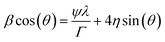
Fig. 1 shows the XRD patterns of SBTi and Nb doped SBTi. All of the peaks were indexed based on orthorhombic cells associated with the A21am space group, which is matched with the JCPDS file number 43-0973.7 No impurity peaks or additional peaks were observed in SBTi and Nb doped SBTi, which clearly indicates that the crystal structure was not affected by Nb doping. However, it could be observed from the XRD patterns of Nb doped SBTi that the strongest (119) peak has slightly shifted towards lower-angle, indicating an expansion in its lattice constant. The lattice expansion in the case of Nd-doped SBTi can be explained on the basis of the larger ionic radii of Nb5+ (0.64 Å) as compared to Ti4+ (0.605 Å).13 The lattice parameters were calculated within the error limit ± 0.002 Å from the Rietveld refinement (profile refinement, Le Bail method) of diffraction data using Jana 2006 software.14 Williamson–Hall relation (eqn (1)) was used for calculating the crystallite size and microstrain parameter.15| |
 | (1) |
where β is the integral breadth of XRD peaks. This was calculated using Jana 2006 (only Lorentzian components). ψ is the Debye–Scherrer constant (0.94 for spherical crystallites), and λ and θ are the incident X-ray wavelength and the diffraction angle respectively. The values of crystallite size (Γ) and microstrain parameter (η) were calculated from the y-intercept and the slope of the βcos(θ) versus sin(θ) plot respectively, as shown in Fig. 2. The details of the reliability factors, lattice parameters, crystallite size and microstrain parameters are listed in Table 1. Fig. 3 shows the SEM images of SBTi and Nb doped SBTi. The surface morphology clearly indicates plate-like structures. The SEM images were analyzed using ImageJ software and grain size (G) and aspect ratios (AR) were calculated. Details are given in Table 1. It is clear from the table that the Nb doping decreases the average grain size and aspect ratio. The decreased grain size may increase the number of grains.
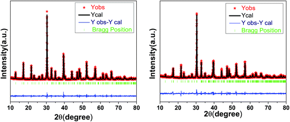 |
| | Fig. 1 XRD patterns of SBTi (left) and Nb doped SBTi (right). | |
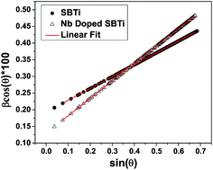 |
| | Fig. 2 Linear fit using the Williamson–Hall relation. | |
Table 1 The details of Rietveld refinements, Williamson–Hall plots, SEM images and the Curie–Weiss law. GOF: goodness of fit, Rwp: weighted profile R-factor, a, b, c: lattice parameters, Γ: crystallite size, η: microstrain, F: tolerance factor G: grain size, AR: aspect ratio, Tc: phase transition temperature, Tθ: Curie temperature, Φ: Curie constant, and ϒ: degree of diffuseness
| Sample |
GOF |
Rwp |
a (Å) |
b (Å) |
c (Å) |
Γ (nm) |
η |
F |
G (μm) |
AR |
Tc (°C) |
Tθ (°C) |
Φ |
ϒ |
| SBTi |
1.74 |
14.22 |
5.442 |
5.453 |
41.012 |
64 |
1.54 × 10⁻³ |
1.00 |
2.65 |
3.80 |
506 |
458 |
0.61 × 10⁵ |
1.11 |
| Nb-SBTi |
2.04 |
17.06 |
5.444 |
5.454 |
41.059 |
43 |
2.27 × 10⁻³ |
0.98 |
1.34 |
3.27 |
448 |
405 |
0.93 × 10⁵ |
1.13 |
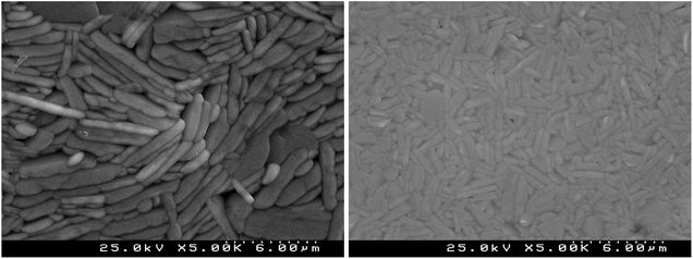 |
| | Fig. 3 SEM images of SBTi (left) and Nb doped SBTi (right). | |
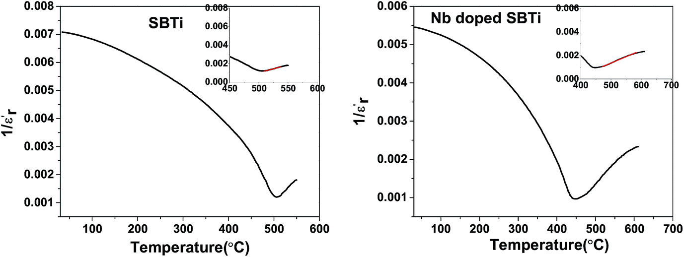
3.2 Dielectric studies
Fig. 4 shows the temperature versus dielectric constant and dielectric loss plot for SBTi and Nb doped SBTi at 1 MHz. From the plots, it is clear that Nb doping enhance the value of the dielectric constant but reduce the Curie temperature. The reduction of the Curie temperature is due to lattice distortion created by Nb doping. The lattice distortion can be calculated from the tolerance factor (F) defined by16| |
 | (2) |
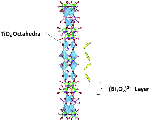
where Δu, Δv, and Δ0 are the radii of the A-cation and B-cation and the radius of the anion respectively. For the calculation we used13 Δu = 1.44 Å (Sr2+), Δv = 0.60 Å (Ti4+) or Δv = 0.64 Å (Nb5+), and Δ0 = 1.40 Å (O2−). The calculated values of F are given in Table 1. The tolerance factor was calculated by assuming SrTiO3 to be undistorted (the effect of Bi2O3 layers has not been taken into account). However, the decreased value of the tolerance factor in the Nb doped case indicated the increase of lattice distortion. The presence of Bi2O3 layers in the SBTi crystal structure has displaced Sr2+ cations, as well as tilted the TiO6 octahedra (shown in Fig. 5). The tilting of TiO6 octahedra is the reason for ferroelectric properties in SBTi.7 The doping at titanium sites can change the tilting of TiO6 octahedra as well as the bond lengths between titanium and oxygen atoms. The Nb doping might be creating more stretching in bond lengths of TiO6 octahedra that itself may be the reason for the increment of the dielectric constant in the Nb doped system. The replacement of less polarizable Ti4+ (electronegativity 1.54) with highly polarizable Nb5+ (electronegativity 1.6) may also be responsible for the increase in the dielectric constant of the Nb doped case. In the dielectric loss versus temperature plot (see Fig. 4), near the transition temperature a kink was observed for both SBTi and Nb doped SBTi. The kink indicates the movement of ferroelectric domain walls.12 The Nb doping decrease the dielectric loss of SBTi, is also evident from the plot. The dielectric data was analysed using the Curie–Weiss law which can be described by the relation| |
 | (3) |
where  is the real part of the relative permittivity or dielectric constant, Tθ is the Curie–Weiss temperature and Φ is the Curie constant. The plot between
  and temperature gives a straight line with a slope of
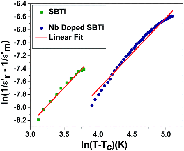
  and the x-axis intercept at Tθ.17 Fig. 6 shows the Curie–Weiss plot of SBTi and Nb doped SBTi at 1 MHz. The solid red line is the linear fit (adjusted R2 > 0.999) obtained for the Curie–Weiss law. The degree of diffuseness (ϒ) of the phase transition is obtained from the modified Curie–Weiss law given below,
| |
 | (4) |
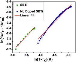
where ϒ is the degree of diffuseness, Φ′ is the Curie-like constant, Tc is the phase transition temperature and  is the maximum value of the dielectric constant at phase transition temperature Tc. The slope of the
  versus ln(T – Tc) plot will give the degree of diffuseness ϒ (Fig. 7).17 The value of (ϒ) generally lies between 1 and 2. If it is close to one, it is indicative of normal phase transition and if close to two, then of diffused phase transition.17 All parameters related to the Curie–Weiss and modified Curie–Weiss laws are calculated and listed in Table 1. From the table, it is clear that the phase transitions are normal phase transitions.
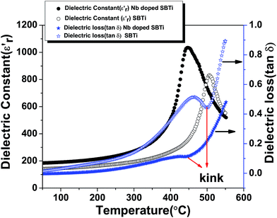 |
| | Fig. 4 Temperature dependence of the dielectric constant and dielectric loss at 1 MHz. | |
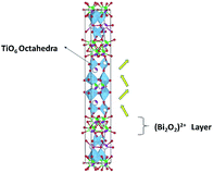 |
| | Fig. 5 Crystal structure of SrBi4Ti4O15, with tilting of TiO6 octahedra shown. | |
 |
| | Fig. 6 Curie–Weiss plots at 1 MHz, SBTi (left) and NbSBTi (right). | |
 |
| | Fig. 7 Modified Curie–Weiss plot at 1 MHz. | |
3.3 Impedance analysis
By the analysis of impedance data one can easily separate the contributions from grains, grain boundaries and electrode effects from the different time constants associated with each function. Fig. 8 shows the Cole–Cole plots of SBTi and Nb doped SBTi. The plots are composed of two semicircular-arcs caused by the electrically different active regions, namely the grains and grain boundaries. The impedance spectra were fitted using an equivalent circuit consisting of two parallel RC elements connected in series. The fitting was performed using Z-view software. The equivalent circuit is shown in the inset of Fig. 8, where R1 is the grain resistance, R2 is the grain boundary resistance, CPE1 is the constant phase element for grains and CPE2 is the constant phase element for grain boundaries. The impedance of constant phase elements can be written as| |
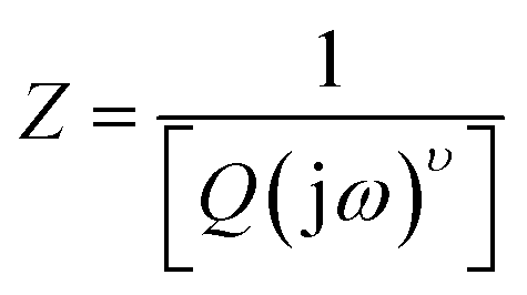
 | (5) |
where  ω is the frequency and Q is a constant with dimensions of farad (second)υ−1. The value of ν represents the magnitude of deviation from the ideal capacitance. It varies from 0 to 1. For an ideal capacitor ν = 1 and for an ideal resistor it is 0. The value of capacitance associated with grains and grain boundaries is obtained from the following formula
| |
 | (6) |
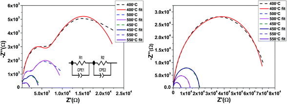 |
| | Fig. 8 Cole–Cole plots in the frequency range of 100 Hz to 1 MHz, SBTi (left) and Nb doped SBTi (right). | |
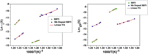
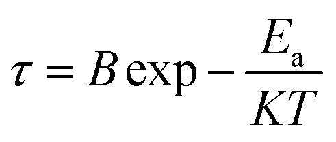
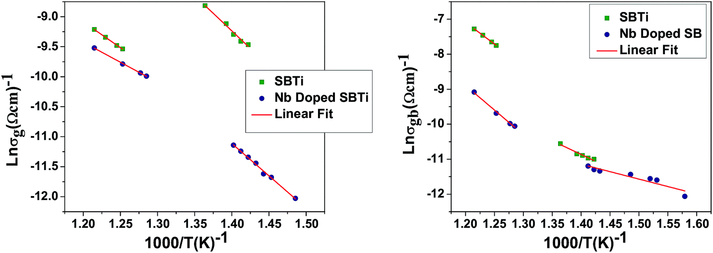
The values of R (R1 and R2), Q (for CPE1 and CPE2) and ν (for CPE1 and CPE2) were obtained from fitting with the equivalent circuit. The obtained parameters from the fitting data were used to evaluate the relaxation time (τ = RC) associated with grains (τg) and grain boundaries (τgb).18 The corresponding Arrhenius equation is given below and the Arrhenius plots are shown in Fig. 9.
| |
 | (7) |
where
B is the pre-exponential factor,
K is the Boltzmann constant,
T is the absolute temperature and
Ea is the activation energy. The following relationship has been used for the calculation of grain (
σg) and grain boundary conductivity (
σgb).
19| |
 | (8) |
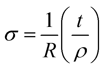
where
σ is the conductivity,
R is the resistance (
R1 or
R2),
t is the thickness and
ρ is the area of the specimen.
19 Electrical conduction is a thermally activated process and follows the Arrhenius law given below.
| |
 | (9) |
where
D is the pre-exponential factor. The Arrhenius plots of grain and grain boundary conductivity are shown in
Fig. 10. The calculated activation energies from grain and grain boundary relaxation times and grain and grain boundary conductivities are given in
Table 2. The reported activation energies based on BaTiO
3 and Bi
2O
3 lattices and their possible reasons are listed in
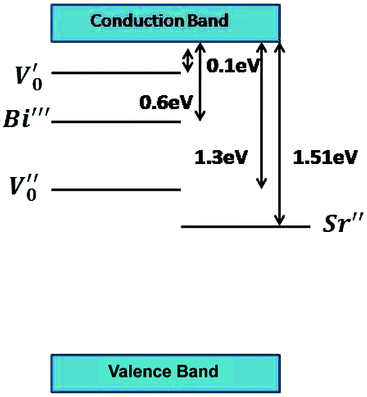
Table 3. Comparison with the table shows that doubly ionized oxygen vacancies, bismuth ion migration and strontium vacancies are present in our samples. A possible representation of the band scheme is given in
Fig. 11.
 |
| | Fig. 9 Arrhenius plot of grain and grain boundary relaxation times. | |
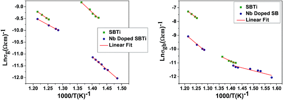 |
| | Fig. 10 Arrhenius plot of grain and grain boundary conductivities. | |
Table 2 Activation energy values (Ea) obtained from Arrhenius plots of grain and grain boundary relaxation times and grain and grain boundary conductivities. τg: relaxation time associated with grains. τgb: relaxation time associated with grain boundaries. σg: grain conductivity. σgb: grain boundary conductivity
| Function |
τg |
τg |
τgb |
τgb |
σg |
σg |
σgb |
σgb |
| Temperature range (°C) |
550–525 |
470–400 |
550–525 |
470–400 |
550–525 |
450–400 |
550–525 |
450–400 |
| Ea (eV) for SBTi |
1.45 |
0.49 |
1.1 |
0.93 |
0.74 |
1.04 |
1.07 |
0.67 |
| Temperature range (°C) |
550–525 |
470–400 |
550–525 |
470–400 |
550–525 |
450–400 |
550–525 |
450–400 |
| Ea (eV) for Nb doped SBTi |
0.57 |
1.58 |
0.89 |
0.56 |
0.47 |
0.57 |
1.1 |
0.95 |
Table 3 Summary of conduction processes and their associated range of activation energy values reported in the literature19–21
| Activation energy range (eV) |
Conduction process |
| 0.7–1.21 |
Diffusion of doubly ionized oxygen vacancies |
| 1.49–1.51 |
Electrons ionized from strontium vacancies |
| 0.1–0.2 |
First ionization energy of oxygen vacancies |
| 15 |
Titanium vacancy migration |
| 2.8 |
Strontium vacancy migration |
| 0.66 |
Activation energy of self-diffusion of bismuth ions |
| 0.18–0.48 |
Conduction by phonon assisted electron/hole hopping |
 |
| | Fig. 11 Schematic diagram of the band scheme. | |
3.4 Grain conductivity
The total bulk grain conductivity (σg) can be expressed as a combination of contributions from mobile ions and electronic charge carriers indicated below.19| |
 | (10) |
where μe, μh, μSr, μTi, μBi and μ0 represent the mobilities of electrons, holes, strontium vacancies, titanium vacancies, bismuth vacancies and oxygen vacancies respectively. The quantities f, p, 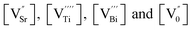 represent the number of electrons, holes, strontium vacancies, titanium vacancies, bismuth vacancies and oxygen vacancies respectively. The quantity e is the electron charge. Cation vacancies (Sr, Bi, Ti) are relatively immobile because of their heavy mass as well as high activation energy. The mobility of the electronic charge carriers is also less because they move by polaronic hopping in the lattice. So, compared to other contributions to the grain conductivity, the oxygen vacancy motion may contribute much more to grain conductivity.
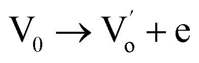
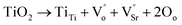
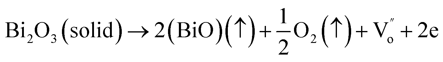
The SBTi ceramics usually contain bismuth vacancies, which is formed during the sintering process. The bismuth vacancy formation is due to its low melting point (∼850 °C). Along with the bismuth vacancy formation, oxygen vacancies also formed to maintain the charge neutrality. The vacancy formation process can be written as Kröger–Vink notation,5
| |
 | (11) |
where

is the doubly ionized oxygen vacancies. Apart from oxygen vacancies due to bismuth loss, high temperature sintering can also lead to the neutral oxygen on regular sites

leaving the lattice, resulting in creating singly or doubly ionized oxygen vacancies. Using the Kröger–Vink notation it can be represented as,
19| |
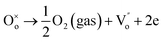 | (12) |
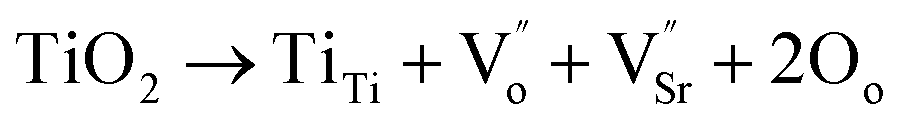
In Nb doped SBTi, the introduction of donor type Nb5+ ions into Ti4+ sites can be written as8
| |
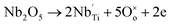 | (13) |
where

is the Nb ion with a +1 effective charge at titanium sites. The two electrons coming from the niobium oxide may reduce the oxygen vacancy, as follows
9| |
 | (14) |
From eqn (14), it is clear that Nb doping decreases the number of oxygen vacancies in the SBTi. This will cause a reduction in the grain conductivity of SBTi. From the Arrhenius plot (Fig. 10) it is clear that Nb doped SBTi shows lower grain conductivity than SBTi. The reduction in the number of oxygen vacancies in Nb doped SBTi is also in line with the activation energy values. The grain conductivity activation energies of SBTi point out the migration of oxygen vacancies (1.04 eV), but for the Nb doped material it is the migration of bismuth ion vacancies (0.57 eV) (refer to Table 2). This mean that a reduction in the number of oxygen vacancies happen in Nb doped SBTi.
3.5 Grain boundary conductivity
The grain boundary conductivity behaviour has been explained using the basic Heywang–Jonker model.22,23 According to the model, the grain boundary consists of back-to-back double Schottky barriers. The grain boundary core is made up of cation vacancies. The cation vacancies attract the nearby electrons and become a negatively charged acceptor states, and as a result, the near interface becomes positive. The near interface contains a positive space charge layer on either side of the grain boundary core. These space charge layers are depleted of mobile charge carriers but contain positive effective charge and defects. These depletion layers create a grain boundary barrier with a barrier height (φ0). The schematic diagram is shown in Fig. 12.
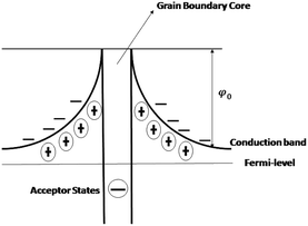 |
| | Fig. 12 Schematic diagram of the grain boundary. | |
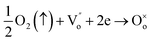
In this case the grain boundary core contains bismuth ion vacancies as well as strontium ion vacancies (acceptor states). The presence of bismuth and strontium ion vacancies was also evident from the activation energies (0.67 and 1.58 eV) (refer to Table 2) The positive space charge layer may be composed of oxygen vacancies. The height of the grain boundary barrier (φ0) can be expressed as,24
| |
 | (15) |
where
e is the electron charge,
ε0 is the permittivity of free space and

is the real part of the relative permittivity of the grain boundary region or the dielectric constant of the grain boundary region,
Nd is the effective concentration of charged dopants in the bulk and
Ns is the concentration of trapped electrons. The relation between the resistivity of the grain boundary (
ρ) and the height of the barrier can be written as
24| |
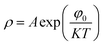 | (16) |
where
A is a geometrical factor,
K is the Boltzmann constant and
T is the absolute temperature. From the Arrhenius plot (
Fig. 10), it is clear that the Nb doped samples show lower grain boundary conductivity than SBTi. The negative temperature coefficient of resistance (NTCR) shown by both SBTi and Nb doped SBTi is also clear from the Arrhenius plot. These observations can be explained using the above model.
From eqn (15), it is clear that the height of the grain boundary barrier (φ0) is inversely proportional to  Therefore the increase in
  will decrease the height of the barrier up to the phase transition temperature (Tc) and thereby a decrease in resistance with temperature is observed up to the phase transition temperature. Above the phase transition temperature, the
  starts to decrease and this will increase the height of the grain boundary. Simultaneously, due to the rise in temperature, the energy of the trapped electrons in the grain boundary also increases. When the energy of the electron traps reaches the Fermi level, trapped electrons start to jump to the conduction band, which can depress the increase in the barrier height as well as the resistance. So, the net effect is the increase in conductivity with temperature above the phase transition temperature.
In the case of Nb doped SBTi, it is clear from eqn (13) that the system acquires an extra electron. These extra electrons do not reduce the oxygen vacancies, as in the case of the grains. However they may fall down the grain boundary core, resulting in an increased concentration of trapped electrons (Ns). This means that the Nb doped SBTi has an increased number of trapped electron concentration (Ns) than SBTi. The increase in trapped electron concentration decreases the grain boundary conductivity. This may be the reason behind the decreased grain boundary conductivity of Nb doped SBTi than SBTi. The calculated activation energies for Nb doped SBTi from the grain boundary conductivity show the presence of oxygen vacancies (0.95 eV and 1.1 eV) (refer to Table 2) in the grain boundaries. This experimental observation also indicates the validity of the above-mentioned model.
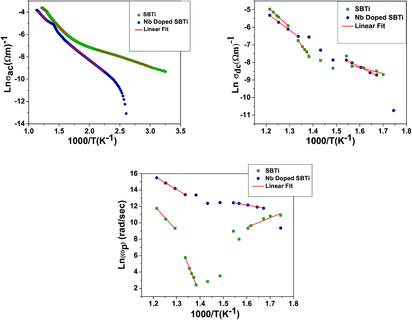
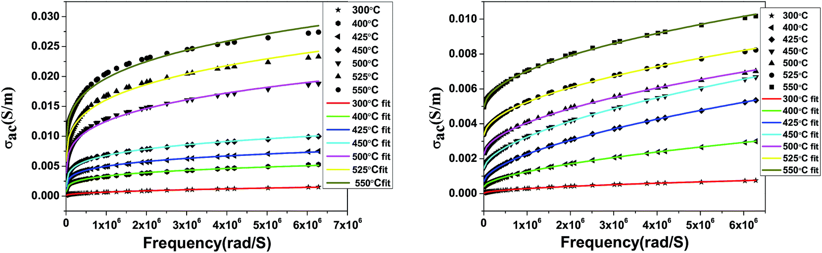
3.6 ac conductivity analysis
3.6.1 ac conductivity and Jonscher’s power law. The response of the ac conductivity with temperature and frequency provides an insight into the different relaxation mechanisms in the material. The ac conductivities of the samples were calculated using the following relation25| |
 | (17) |
where ε0 is the permittivity of free space, ω is the frequency,  is the dielectric constant and tanδ is the dielectric loss. The frequency dependence of the ac conductivity shows two regions (see Fig. 13): one is frequency independent and the other is frequency dependent. This behaviour can be explained using Jonscher’s universal power law. The ac conductivity plots at different temperatures were fitted using Jonscher’s universal power law described below,25
| |
 | (18) |
where σdc, A, and n are the bulk dc conductivity, the pre-exponential factor and the frequency exponent respectively. Fig. 13 shows the ac conductivity versus frequency plots at different temperatures along with fitted curves of Jonscher’s power law. The mathematical fitting was performed using OriginPro8.5 with a non-linear curve fitting method. The values of σdc, A and n were obtained from the fitted curves.
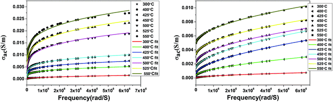 |
| | Fig. 13 ac conductivity with frequency along with fitting curves of the power law; SBTi (left) and Nb doped SBTi (right). | |
The obtained values of the frequency exponent (n) in SBTi and Nb doped SBTi is less than 1, indicating the non-Debye behaviour of the samples. It also shows that the charge carriers undergo a translational motion with sudden hopping.26 The pre-exponential factor A determines the strength of polarizability.27 From Fig. 14, it is clear that compared to SBTi the Nb doped SBTi shows a decrease in A values. This indicates that Nb doping reduces the polarizability of SBTi. The relation between polarizability (α) and dielectric constant is given by (assuming that the atoms are the same kind)28
| |
 | (19) |
where
ε0 is the permittivity of free space,

is the dielectric constant and
z is the number of atoms per unit volume. It is clear from the previous section that the Nb doping reduces the number of oxygen vacancies in SBTi. This decrease in the number of oxygen vacancies will increase the value of
z in Nb doped SBTi, which in turn causes a decrease in polarizability of Nb doped SBTi. This may be the reason behind the decreased value of
A in Nb doped SBTi. However, previous studies by Hao
et al.1 show that there is increase in the value of electric polarization of Nb doped SBTi when compared to un-doped SBTi. The polarization (
p) of the whole sample can be expressed by the relation,
28| |
 | (20) |
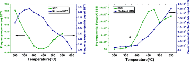 |
| | Fig. 14 The plots between the frequency exponent (n) versus temperature (left) and the pre-exponential factor (A) versus temperature (right). | |
This expression is a summing over all atomic positions where α is the polarizability and Elocal is the local electric field at the atomic site. Even though the polarizability (α) of the Nb doped SBTi decreases, the z and Elocal values are increasing. This may lead to an increment in the polarization of Nb doped SBTi. The increase in the local electric field (Elocal) is due to the replacement of less polarizable Ti4+ (electronegativity 1.54) with highly polarizable Nb5+ (electronegativity 1.6) ions.
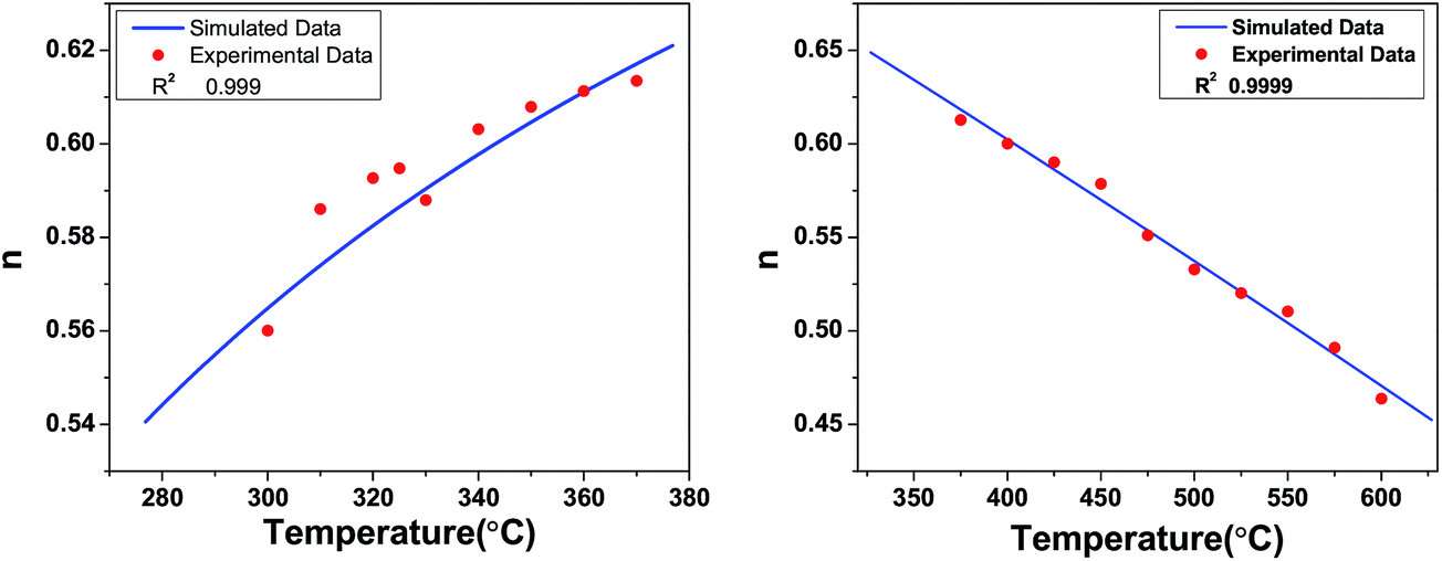
3.6.2 Mechanism of ac conduction. The behaviour of n versus temperature plots (Fig. 14) tells us about the ac conductivity mechanism. The variation of n with temperature can be directly correlated to the theoretical models of ac conductivity, and Table 4 shows the details. From the table, one can conclude that none of the models completely match with the experimental observations. However, the ac conductivity mechanism can be explained using two models at different temperature regions. In the case of SBTi, large-polaron QMT, and small-polaron QMT models have been used, whereas in the case of Nb doped SBTi, small-polaron QMT and Correlated Barrier Hopping (CBH) models have been used to explain the ac conductivity mechanism. All the mathematical fitting in this section was done using Wolfram Mathematica 10.
Table 4 Summary of co-relations between ac conductivity models and the functional dependence of the frequency exponent (n) with temperature29
| Model name |
Variation of frequency exponent (n) with temperature |
| Quantum Mechanical Tunneling (QMT) |
n = 0.81, independent of temperature |
| Small-polaron QMT |
Increasing n with increasing temperature |
| Large-polaron QMT |
(1) High value of the polaron radius: n exhibits a minimum at a certain temperature and subsequently increases in a fashion similar to small-polaron QMT |
| (2) Low value of the polaron radius: decreasing n with increasing temperature, but much steeper than CBH |
| Hopping Over a Barrier (HOB) |
n = 1, independent of temperature |
| Correlated Barrier Hopping (CBH) |
Decreasing n with increasing temperature |
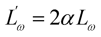
According to the large-polaron QMT model, the frequency exponent (n) can be written as,29
| |
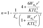 | (21) |
The  and r′ = 2αr are the reduced quantities where α is the polarizability, Lω is the tunnelling distance at a frequency ω and r is the polaron radius. K and T are the Boltzmann constant and temperature respectively. The polaron hopping energy (WH) is given by
| |
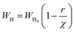 | (22) |
where
WH0 is a parameter, and
χ is the interatomic spacing.
Eqn (21) is used to fit with the
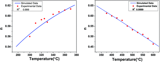
n versus temperature curve of SBTi, in the temperature range 300 °C to 400 °C (see
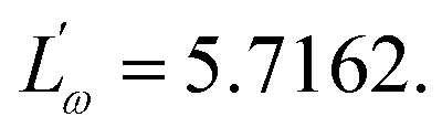
Fig. 15). The obtained parameters from the fitting curve are
WH0 = −0.1340 eV and

The parameter
r′ = 7 was assumed for the fitting. The higher temperature region was fitted using the small-polaron QMT model.
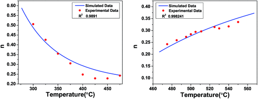 |
| | Fig. 15 Frequency exponent versus temperature for SBTi, fitted with the large-polaron QMT model (left) and the small-polaron QMT model (right). | |
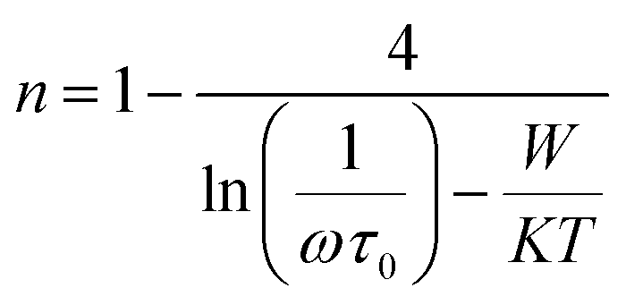
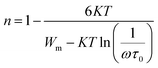
From the small-polaron QMT model, the relation between the frequency exponent (n) and the temperature (T) can be written as,29
| |
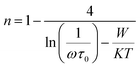 | (23) |
where
ω is the frequency,
τ0 is the relaxation time,
K is the Boltzmann constant and
W is the polaron hopping energy. The
n versus temperature curve of SBTi in the temperature range 450 °C to 550 °C was fitted with
eqn (23) (see
Fig. 15). The obtained value of the polaron hopping energy (
W) from the fitted curve is 0.702 eV. The values of
ω = 10
5 Hz and
τ0 = 10
−12 s were assumed for the fitting.
The variation of the frequency exponent (n) with temperature for Nb doped SBTi is also fitted with eqn (23), in the temperature range 300 °C to 375 °C (see Fig. 16). The values of ω = 105 Hz and τ0 = 10−14 s were assumed for the fitting and the obtained value of the polaron hopping energy (W) is 0.570 eV. The higher temperature range was fitted with the CBH model (see Fig. 16). The relation between n and the temperature from the CBH model is given below,29
| |
 | (24) |
where
ω is the frequency,
τ0 is the relaxation time,
K is the Boltzmann constant and
Wm is the barrier height. The obtained values of
Wm and
τ0 from the fitted curve are 0.951 eV and 2.710 × 10
−6 s respectively. The value of
ω = 10
5 Hz was assumed for the fitting.
 |
| | Fig. 16 Frequency exponent versus temperature for Nb doped SBTi, fitted with the small-polaron QMT model (left) and the CBH model (right). | |
The parameters and the activation energies from the fitting are physically possible values and this proves the validity of the models. Note that the changes in conduction mechanism which occur in both samples are in the vicinity of the Curie–Weiss temperature (458 °C and 405 °C). The Curie–Weiss temperature is that at which the change in crystal structure occurs. It is important to note that in the ferroelectric region, the conduction mechanism in SBTi is large-polaron but is small-polaron for Nb doped SBTi. The main difference between the large-polaron and small-polaron models is related to the spreading of lattice distortion. If the lattice distortions spread over many lattice sites, then it is called large-polaron. If the distortions are limited to the nearest neighbouring ions, then it is small-polaron.30 Therefore, the change in the conduction mechanism indicates the reduction of lattice distortions in Nb doped SBTi. This again leads to the conclusion that the number of oxygen vacancies has been reduced by niobium doping.
3.6.3 ac conductivity in terms of hopping frequency. For further understanding of the relaxation process, we analyzed the ac conductivity response with temperature using the Arrhenius law given below| |
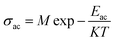 | (25) |
where M is the ac conductivity pre-exponential factor, K is the Boltzmann constant and Eac is the ac conductivity activation energy. Fig. 17 shows the Arrhenius plot and the activation energies are given in Table 5. The activation energy obtained can be correlated with the possible conduction processes given in Table 3. The activation energy in the low temperature (180–35 °C) region of SBTi indicates the presence of singly ionized oxygen vacancies, and it can be represented as7| |
 | (26) |
| |
 | (27) |
 |
| | Fig. 17 Arrhenius plots of ac conductivity, dc conductivity and hopping frequency at 1 MHz. | |
Table 5 Activation energy values obtained from the Arrhenius plots of ac conductivity, bulk dc conductivity and hopping frequency. Eac: ac conductivity activation energy, Edc: dc conductivity activation energy, and Ep: activation energy for hopping frequency
| Activation energy (eV) |
Eac |
Eac |
Eac |
Edc |
Edc |
Edc |
Ep |
Ep |
Ep |
| Temperature range (°C) |
550–525 |
490–350 |
180–35 |
550–525 |
475–450 |
375–300 |
550–525 |
475–450 |
375–300 |
| For SBTi |
0.34 |
0.51 |
0.15 |
1.05 |
1.63 |
0.43 |
2.68 |
6.04 |
1.15 |
| Activation energy (eV) |
Eac |
Eac |
Edc |
Edc |
Ep |
Ep |
| Temperature range (°C) |
550–525 |
490–350 |
550–475 |
375–325 |
550–475 |
375–325 |
| For Nb doped SBTi |
0.51 |
0.37 |
0.85 |
0.57 |
1.45 |
0.44 |
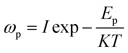
At high temperatures the singly ionized oxygen may become doubly ionized oxygen vacancies (eqn (27)). The presence of doubly ionized oxygen vacancies at high temperature is evident from the activation energies obtained from various functions (Tables 5 and 2). Apart from the bismuth vacancy migration (0.51 eV), the phonon-assisted electron or hole hopping also happens in our samples (0.34 eV and 0.37 eV) (Table 5). The possible mechanism for the phonon-assisted electron or hole hopping might be the valence fluctuations of Ti4+/Ti3+ ions. In the Nb doped SBTi, 5% of Ti4+ ions were replaced with Nb5+ ions. This will effectively decrease the ac conductivity contributed from valency fluctuations of Ti4+/Ti3+ ions. This leads to a decrease in ac conductivity of Nb doped SBTi as seen in Fig. 13. The power law expressed in hopping frequency (ωp) is31
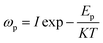
| |
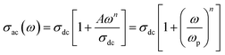 | (28) |
| |
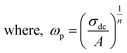 | (29) |
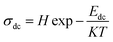
The hopping frequency is the frequency at which the conductivity relaxation begins to appear. In general, σdc (bulk dc conductivity) and ωp are thermally activated parameters and follow the Arrhenius laws given below,31
| |
 | (30) |
| |
 | (31) |
where
H is the dc conductivity pre-exponential factor,
K is the Boltzmann constant,
Edc is the dc conductivity activation energy,
I is the pre-exponential of hopping frequency and
Ep is the activation energy for hopping frequency. The corresponding activation energies are obtained from the Arrhenius plots (
Fig. 17). The calculated activation energies are listed in
Table 5. The activation energy obtained (
Table 5) can be correlated with the possible conduction process (
Table 3).
The activation energy values Edc and Ep are not the same, and this shows that the charge carriers has to overcome different energy barriers while conducting and relaxing. The reason for the activation energy of 6 eV (475–450 °C in SBTi) is a confusing matter, even though the reported activation energies from titanium based half-Heusler compounds show that 5–6 eV is due to self-diffusion of titanium ions.32 But, it is worth to note that the reported activation energy for titanium vacancy migration in BaTiO3 is 15 eV.19 The activation energy from various functions also points to the strontium vacancy formation and migration of strontium vacancies in SBTi and Nb doped SBTi. In SBTi, there is a possibility of excess accommodation of titanium ions in the lattice, which can lead to the formation of doubly ionized strontium vacancies. This can be represented as,21
| |
 | (32) |
In the Nb doped SBTi, the excess charge of Nb5+ is compensated in two ways, one is through the formation of conduction electrons (which will reduce oxygen vacancies) and the second is by strontium vacancies.
4 Conclusions
The SBTi and Nb doped SBTi ceramics have been successfully synthesized using solid state reactions. The XRD pattern shows that the Nb substitution does not change the crystal structure of SBTi. The observed phase transitions are normal. The Nb substitution decreases the transition temperature of SBTi (506 °C to 448 °C) but increases the dielectric constant. The relaxation times and grain and grain boundary conductivities have been obtained from fitted parameters of the Cole–Cole plots. The grain boundary conductivity was analyzed in the light of the Heywang–Jonker model. The Heywang–Jonker model was successful in the case of BaTiO3 ceramics and we extended it to bismuth layered oxides. The frequency dependent ac conductivity at different temperatures has been analyzed using Jonscher’s power law. Many authors have explained the ac conductivity in view of Jonscher’s power law but in the current article we correlated the frequency exponent (n) with ac conductivity models. Taking into consideration the models, we concluded that the conduction mechanism of SBTi from 300 °C to 475 °C is large-polaron tunneling and from 475 °C to 550 °C is small-polaron tunneling. For the Nb doped case, the conduction mechanism from 300 °C to 375 °C is small-polaron tunneling and from 375 °C to 550 °C is correlated band hopping. Furthermore, Jonscher’s power law has been used for calculating the hopping frequency and activation energies associated with it. The activation energies evaluated from different functions indicate that the conductivity in the SBTi sample has contributions from the migration of singly and doubly ionized oxygen vacancies, bismuth ion vacancies, electrons ejected from strontium ions, strontium ion vacancies and valance fluctuations of Ti4+/Ti3+ ions. From the analysis of activation energies, ac conductivity models, and Jonscher’s power law, we concluded that donor ion Nb5+ doping in SBTi reduces the defects originating from oxygen vacancies. The reduction in oxygen vacancies might be the reason for the improved electrical properties of Nb doped SBTi.
Conflicts of interest
There are no conflicts to declare.
Acknowledgements
Venkata Saravanan acknowledges the facilities provided by CUTN, UGC for the start-up grant, DST-SERB for the Early Career Research grant (ECR/2015/ 000273), and the University of Aveiro, Fundaçã para a Ciência e a Tecnologia (FCT), Portugal for the financial support through the grants PTDC/CTM/71643/2006 and SFRH/BPD/80742/2011. Muhammad Asif acknowledges the support of the Department of MME, UET, Lahore. Roshan and Vineetha acknowledge the facilities and financial support provided by CUTN.
Notes and references
- H. Hao, H. Liu and S. Ouyang, J. Electroceram., 2009, 22, 357–362 CrossRef CAS.
- P. Nayak, T. Badapanda and S. Panigrahi, J. Mater. Sci.: Mater. Electron., 2017, 28, 625–632 CrossRef CAS.
- H. Zou, Y. Hu, X. Zhu, Y. Sui, X. Wang and Z. Song, Ferroelectrics, 2015, 488, 62–70 CrossRef CAS.
- D. Peng, H. Zou, C. Xu, X. Wang, X. Yao, J. Lin and T. Sun, AIP Adv., 2012, 2, 042187 CrossRef.
- P. Nayak, T. Badapanda, S. Anwar and S. Panigrahi, Phase Transitions, 2015, 88, 430–444 CrossRef CAS.
- D. Shan, X.-f. Qian, W. Wang and X.-b. Chen, Integr. Ferroelectr., 2007, 94, 64–72 CrossRef CAS.
- P. Nayak, T. Badapanda, A. K. Singh and S. Panigrahi, RSC Adv., 2017, 7, 16319–16331 RSC.
- C. Jin, J. Zhu, X.-y. Mao, J.-h. He, J.-c. Shen and X.-b. Chen, Integr. Ferroelectr., 2006, 85, 39–47 CrossRef.
- C. Jin, C.-p. Du, J. Zhu, J.-h. He, X.-y. Mao and X.-b. Chen, J. Phys. D: Appl. Phys., 2006, 39, 2415 CrossRef CAS.
- J. Zhu, X.-y. Mao and X.-b. Chen, Solid State Commun., 2004, 130, 363–366 CrossRef CAS.
- Q. Wang, Z.-P. Cao, C.-M. Wang, Q.-W. Fu, D.-F. Yin and H.-H. Tian, J. Alloys Compd., 2016, 674, 37–43 CrossRef CAS.
- P. Nayak, T. Badapanda and S. Panigrahi, J. Mater. Sci.: Mater. Electron., 2016, 27, 1217–1226 CrossRef CAS.
- R. D. Shannon, Acta Crystallogr., Sect. A: Cryst. Phys., Diffr., Theor. Gen. Crystallogr., 1976, 32, 751–767 CrossRef.
- V. Petříček, M. Dušek and L. Palatinus, Z. Kristallogr., 2014, 229, 345–352 Search PubMed.
- S. Kumar, I. Coondoo, M. Vasundhara, A. K. Patra, A. L. Kholkin and N. Panwar, J. Appl. Phys., 2017, 121, 043907 CrossRef.
- X. Liu, R. Hong and C. Tian, J. Mater. Sci.: Mater. Electron., 2009, 20, 323 CrossRef CAS.
- T. Shet, R. Bhimireddi and K. Varma, J. Mater. Sci., 2016, 51, 9253–9266 CrossRef CAS.
- C. Hsu and F. Mansfeld, Corrosion, 2001, 57, 747–748 CrossRef CAS.
- I. Coondoo, N. Panwar, R. Vidyasagar and A. L. Kholkin, Phys. Chem. Chem. Phys., 2016, 18, 31184–31201 RSC.
- S. Otake, Y. Ishii and N. Matsuno, Jpn. J. Appl. Phys., 1981, 20, 1037 CrossRef CAS.
- S.-H. Kim, J.-H. Moon, J.-H. Park, J.-G. Park and Y. Kim, J. Mater. Res., 2001, 16, 192–196 CrossRef CAS.
- W. Heywang, J. Am. Ceram. Soc., 1964, 47, 484–490 CrossRef CAS.
- G. Jonker, Solid-State Electron., 1964, 7, 895–903 CrossRef CAS.
- Y. Chen and S. Yang, Adv. Appl. Ceram., 2011, 110, 257–269 CrossRef CAS.
- P. Nayak, T. Badapanda and S. Panigrahi, J. Mater. Sci.: Mater. Electron., 2015, 26, 2913–2920 CrossRef CAS.
- T. V. Kumar, A. S. Chary, S. Bhardwaj, A. Awasthi and S. N. Reddy, Int. J. Mater. Sci. Appl., 2013, 2, 173–178 CAS.
- N. Panda, B. Parida, R. Padhee and R. Choudhary, J. Mater. Sci.: Mater. Electron., 2015, 26, 3797–3804 CrossRef CAS.
- R. Puri and V. Babbar, Solid state physics and electronics, S. Chand, 1998 Search PubMed.
- S. Elliott, Adv. Phys., 1987, 36, 135–217 CrossRef CAS.
- J. Devreese, arXiv preprint cond-mat/0004497, 2000.
- C. Mariappan, G. Govindaraj, S. V. Rathan and G. V. Prakash, Mater. Sci. Eng., B, 2005, 121, 2–8 CrossRef.
- A. Page, A. Van der Ven, P. Poudeu and C. Uher, J. Mater. Chem. A, 2016, 4, 13949–13956 RSC.
Footnote |
| † Electronic supplementary information (ESI) available. See DOI: 10.1039/c8ra06621c |
|
| This journal is © The Royal Society of Chemistry 2018 |
Click here to see how this site uses Cookies. View our privacy policy here. 
 Open Access Article
 This Open Access Article is licensed under a Creative Commons Attribution-Non Commercial 3.0 Unported Licence
 a,
Vineetha P.a,
Muhammad Asif Rafiqb and
Venkata Saravanan K
a,
Vineetha P.a,
Muhammad Asif Rafiqb and
Venkata Saravanan K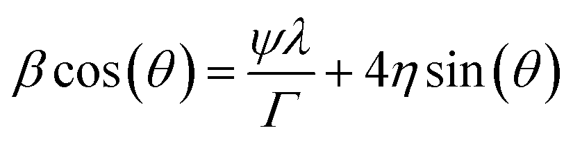


 is the real part of the relative permittivity or dielectric constant, Tθ is the Curie–Weiss temperature and Φ is the Curie constant. The plot between
  and temperature gives a straight line with a slope of
  and the x-axis intercept at Tθ.17 Fig. 6 shows the Curie–Weiss plot of SBTi and Nb doped SBTi at 1 MHz. The solid red line is the linear fit (adjusted R2 > 0.999) obtained for the Curie–Weiss law. The degree of diffuseness (ϒ) of the phase transition is obtained from the modified Curie–Weiss law given below,
 is the maximum value of the dielectric constant at phase transition temperature Tc. The slope of the
  versus ln(T – Tc) plot will give the degree of diffuseness ϒ (Fig. 7).17 The value of (ϒ) generally lies between 1 and 2. If it is close to one, it is indicative of normal phase transition and if close to two, then of diffused phase transition.17 All parameters related to the Curie–Weiss and modified Curie–Weiss laws are calculated and listed in Table 1. From the table, it is clear that the phase transitions are normal phase transitions.

 ω is the frequency and Q is a constant with dimensions of farad (second)υ−1. The value of ν represents the magnitude of deviation from the ideal capacitance. It varies from 0 to 1. For an ideal capacitor ν = 1 and for an ideal resistor it is 0. The value of capacitance associated with grains and grain boundaries is obtained from the following formula


 represent the number of electrons, holes, strontium vacancies, titanium vacancies, bismuth vacancies and oxygen vacancies respectively. The quantity e is the electron charge. Cation vacancies (Sr, Bi, Ti) are relatively immobile because of their heavy mass as well as high activation energy. The mobility of the electronic charge carriers is also less because they move by polaronic hopping in the lattice. So, compared to other contributions to the grain conductivity, the oxygen vacancy motion may contribute much more to grain conductivity.
 is the doubly ionized oxygen vacancies. Apart from oxygen vacancies due to bismuth loss, high temperature sintering can also lead to the neutral oxygen on regular sites
  leaving the lattice, resulting in creating singly or doubly ionized oxygen vacancies. Using the Kröger–Vink notation it can be represented as,19

 is the Nb ion with a +1 effective charge at titanium sites. The two electrons coming from the niobium oxide may reduce the oxygen vacancy, as follows9


 is the real part of the relative permittivity of the grain boundary region or the dielectric constant of the grain boundary region, Nd is the effective concentration of charged dopants in the bulk and Ns is the concentration of trapped electrons. The relation between the resistivity of the grain boundary (ρ) and the height of the barrier can be written as24
 Therefore the increase in
  will decrease the height of the barrier up to the phase transition temperature (Tc) and thereby a decrease in resistance with temperature is observed up to the phase transition temperature. Above the phase transition temperature, the
  starts to decrease and this will increase the height of the grain boundary. Simultaneously, due to the rise in temperature, the energy of the trapped electrons in the grain boundary also increases. When the energy of the electron traps reaches the Fermi level, trapped electrons start to jump to the conduction band, which can depress the increase in the barrier height as well as the resistance. So, the net effect is the increase in conductivity with temperature above the phase transition temperature.
 is the dielectric constant and tan

 is the dielectric constant and z is the number of atoms per unit volume. It is clear from the previous section that the Nb doping reduces the number of oxygen vacancies in SBTi. This decrease in the number of oxygen vacancies will increase the value of z in Nb doped SBTi, which in turn causes a decrease in polarizability of Nb doped SBTi. This may be the reason behind the decreased value of A in Nb doped SBTi. However, previous studies by Hao et al.1 show that there is increase in the value of electric polarization of Nb doped SBTi when compared to un-doped SBTi. The polarization (p) of the whole sample can be expressed by the relation,28
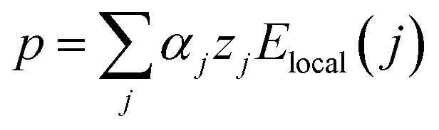


 and r′ = 2αr are the reduced quantities where α is the polarizability, Lω is the tunnelling distance at a frequency ω and r is the polaron radius. K and T are the Boltzmann constant and temperature respectively. The polaron hopping energy (WH) is given by
 The parameter r′ = 7 was assumed for the fitting. The higher temperature region was fitted using the small-polaron QMT model.