
 Open Access Article
 This Open Access Article is licensed under a Creative Commons Attribution-Non Commercial 3.0 Unported Licence
Negative-capacitance and bulk photovoltaic phenomena in gallium nitride nanorods network
Atul Thakre ab,
Sunil Singh Kushvahaab,
M. Senthil Kumarab and
Ashok Kumar*ab
ab,
Sunil Singh Kushvahaab,
M. Senthil Kumarab and
Ashok Kumar*ab
aAcademy of Scientific and Innovative Research (AcSIR), CSIR-National Physical Laboratory Campus, Dr. K. S. Krishnan Marg, New Delhi 110012, India. E-mail: ashok553@nplindia.org
bCSIR-National Physical Laboratory, Dr. K. S. Krishnan Marg, New Delhi 110012, India
First published on 21st September 2018
Abstract
An enhanced self-powered near-ultraviolet photodetection phenomenon was observed in epitaxial gallium nitride (GaN) nanorods network grown on an intermediate layer of N:GaN on a nitridated HfO2(N:HfO2)/SiO2/p-Si substrate. The fabricated Au/GaN/N:GaN/N:HfO2/Ag heterostructure exhibited a giant change (OFF/ON ratio > 50 without applying any external electrical field) in its conductance when illuminated by a very weak (25 mW cm−2) near-UV monochromatic light with a low dark current (nearly 20 nA). The presented near-UV photodetector offers photoresponsivity of ∼2.4 mA W−1 at an applied voltage of 1 V. We observed an optically generated internal open circuit voltage of ∼155 mV and short circuit current ∼430 nA, which can be attributed to the quantum confinement of free charge carriers in the nanorod matrix. Interestingly, it also shows a negative capacitance after near-UV illumination. It has great potential as a self-powered UV photodetector and in metamaterial applications.
Introduction
Gallium nitride-based semiconductor thin films have been widely studied for optoelectronic devices such as light emitting diodes (LEDs), lasers, high electron mobility transistors (HEMT), photo-detectors, high temperature and high power electronic devices applications.1–9 The vast popularity of GaN for these applications is due to its direct band gap, bandgap tunability, chemical and thermal stability. Apart from the GaN's smooth, thin films, several nanostructures such as nanowalls, nanorods, nanotubes, nanorods, etc. have also been extensively studied for various application purposes.10–15 Among these, nanorods have attracted the scientific community due to their superior functionalities, lateral continuity, and porosity, which offer potential applications such as nitride based sensors and devices.16–18 The ultraviolet (UV) photo-detection has drawn extensive attention due to its broad application in several instruments, industries, etc. The UV region can be divided into three spectral regions; (1) UV-A (λ is from 400 to 320 nm), (2) UV-B (λ is from 320 to 280 nm), and (3) UV-C (λ is from 280 to 200 nm).19–21 The UV radiation detection offers various applications in the field of chemical, environmental, flame detection, astronomical and optical studies. For example, flame detection in the hot engine requires thermally stable high-performance detectors. The Si-based UV detectors have some limitations because of its energy bandgap (1.1 eV), phosphors are required to attenuate high energy photons, expensive high pass optical filters. Thus the devices degraded at high temperature due to low efficiency and increased dark current.22 Since the GaN based detectors do not need filters, and stability at high temperature; it has emerged as a potential candidate as wide band gap UV photo detectors.23 Though, various GaN nanostructures have been studied and reported for the UV photo detection application, the GaN nanorods network geometry based UV detectors have attracted considerable interest owing to its higher sensitivity of light due to higher surface to volume ratio, and small size is comparable to the Debye length.24 Soci et al.25 and Yang et al.26 reported the enhanced photosensitivity in the 1D nanorods network of ZnO UV photodetectors. Similarly, GaN-based nanorods networks have also been reported for the application as UV photo detectors.3,27–29 Comparably, The GaN nanostructures with direct band gap based UV photo-detectors offer several superior features such as stability at high temperature, low dark current, excellent optical and electrical properties, high current mobility and superior chemical stability over its competitors.30 In spite of all these superiorities, the GaN-based UV photo-detectors need further advancements in optoelectronic performance such as sensitivity and increase photocurrent intensity. Some groups have reported incorporation of metal nanoparticles such as Au, Ag, and Pt, etc. to enhance the performance of the photo detection.29,31–33In this work, an intermediate layer of N:GaN between GaN nanorods and HFO, using the nitridation process, is grown to stop the excess transportation of oxygen ions from HFO to GaN; thus lowering down the dark current. The nitridated layer also forms an intermediate N:GaN layer which has greater lattice matching with that of GaN; thus offers excellent epitaxial nanorods geometry for the UV photodetection. The three security layers, i.e., N:GaN, high-k HFO, and SiO2 layers protect any photocurrent injected from the bottom silicon substrate. We report the enhanced UV photodetection in epitaxial Au/GaN/GaN:N/HfO2/Ag heterostructure with an ON/OFF ratio > 50 without any bias voltage.
Experimental
The thin HfO2 layer on p-Si was deposited by atomic layer deposition (ALD) technique. The high energy (400 W of r.f. forward power) nitrogen plasma was used for the nitridation of the HfO2 surface. The nitridation phenomenon takes place at substrate temperature of 700 °C in presence of active nitrogen radicals for 35 min. A detailed growth process has been reported elsewhere.34,35 The GaN film was grown on pre-nitridated HfO2 (5 nm) buffer layered Si (100) substrate using laser-assisted molecular beam epitaxy (LMBE) technique. A high purity hydride vapor phase epitaxy grown polycrystalline solid GaN target (99.9999%) was ablated using a KrF excimer laser (λ: 248 nm, pulse width: 25 ns) with laser energy density of ∼2 J cm−2. Growth was performed in the presence of a constant r.f. nitrogen plasma environment using semiconductor grade nitrogen gas with a flow rate of ∼0.4 sccm and r.f. power of 250 W. The growth temperature and duration for GaN film are 700 °C and 3 h, respectively. The surface morphology of the GaN film was obtained using a field emission scanning electron microscopy (FESEM) operated at 5 kV. The photoluminescence (PL) property of the sample has been studied using He–Cd laser (λ: 325 nm) as an excitation source at room temperature. To carry out the electrical measurements, semitransparent gold electrodes having circular patterning with a diameter of 200 μm were sputtered through a shadow mask. In the measurements, a Keithley 236 source meter unit, a Precision Multiferroic Tester (Radiant Technologies Inc.) and a Hioki 3532-50 LCR Hi-Tester coupled with the microprobe system were employed. A weak UV laser source (λ: 405 nm) with energy density 25 mW cm−2 was employed to check the photocurrent. The current–voltage measurement was carried out using top Au electrode as positively bias voltage.Results and discussion
The LMBE grown GaN nanorods network surface morphology was characterized using FESEM technique. Fig. 1(a) shows the high magnification 45° tilt view FESEM image depicting excellent vertical geometry of nanorods having average diameter of ∼100 to 150 nm.34 Also, Fig. 1(b) shows the PL spectrum recorded for the GaN nanorods network at 325 nm excitation. The PL spectra show the peak centered at ∼362 nm (Eg ≈ 3.42 eV) along with a broad yellow luminescence (YL) band ranging between 520–600 nm and centered around 540 nm (2.29 eV).36 During the growth of the GaN nanorods, initially the growth parameters and conditions favor the formation of GaN thin film, and then it forms an island structure which later favors the formation of GaN nanorods. The GaN nanorods are polycrystalline in nature, however most of the lattice planes are oriented along GaN (0002) plane. These results suggest good quality nanorods having relatively high density nearly 5.5 × 10⁹ nanorods per sq cm and aspect ratio nearly 1![[thin space (1/6-em)]](https://www.rsc.org/images/entities/char_2009.gif) :1.2. The large area EDAX data provide Ga:N ratio nearly 46:54 (±3).34
:1.2. The large area EDAX data provide Ga:N ratio nearly 46:54 (±3).34
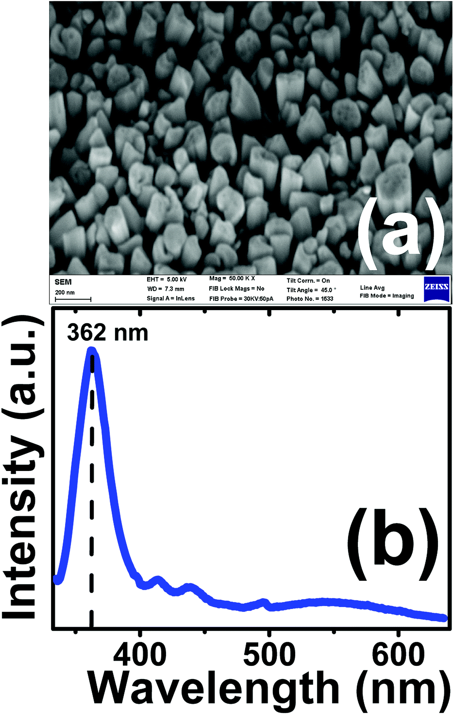 | ||
| Fig. 1 (a) Depicts the FESEM image of the top surface of GaN/N:GaN/N:HfO2/SiO2/p-Si heterostructure nanorods network epitaxially grown on nitridated HfO2 buffer layer, and (b) Photoluminescence (PL) spectra of GaN nanorods network at 325 nm excitation. | ||
The photoresponse in the current–voltage (I–V) characteristics of the Au/GaN/N:GaN/N:HfO2/Ag heterostructure have been investigated with keeping the top semitransparent Au electrode as the drive electrode. A closed-loop voltage sweep of −5 V → +5 V → −5 V was applied across the one dimensional (1D) heterostructure capacitive device with a complete dark and UV light condition; as shown in Fig. 2(a). The I–V plot shows a diode-like behavior in the dark condition, i.e., it exhibits high resistive behavior when the top Au is positively biased. To rule out any photocurrent effect from the bottom p-Si/SiO2 interface, we have drawn current from the N:GaN/N:HfO2/Ag interface. The current across Au/GaN nanorods is almost one order smaller than the N:HfO2/Ag interface. However, an anomalous enhancement in photocurrent was observed under illumination. Additionally, the nitridated HfO2 layer prevents any contribution of the bottom Si. In our previous report, we have investigated the I–V characteristics in Au/HfO2/SiO2/Si with the tungsten filament bulb in illuminated and dark conditions.37 In this investigation, the I–V characteristics exhibited the several order increment in current on both side of the polarity when illuminated; whereas the present scenario, the I–V characteristics shows no change in the current on negative side of the polarity when illuminated and huge change on the positive side of the applied voltage polarity. Additionally, the capacitance vs. voltage plot shows the hysteresis between voltage sweeps of nearly −3 V to 3 V, whereas in the present scenario, GaN nanorods show negative capacitance under small bias voltage. Thus, it clearly rules out any contribution of the bottom Si/SiO2 layer in the conduction in the present proposed Au/GaN/N:GaN/N:HfO2/Ag system.
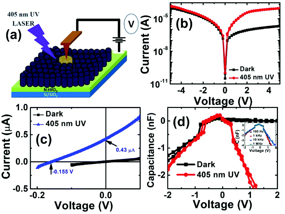 | ||
| Fig. 2 (a) Schematic of Au/GaN/N:GaN/N:HfO2/Ag photo-detector device. Here, to maximize the charge collection, the nanorods have been 3-dimensionally coated with the semi-transparent Au electrode. (b) and (c) show the I–V characteristics in dark and near-UV illumination with internally generated open circuit voltage of 155 mV and short circuit current of 430 nA, and (d) Capacitance vs. voltage plot for the device in dark and near-UV illumination (inset image shows the capacitance plot with different frequencies under the UV exposure). | ||
When the near-UV monochromatic laser light incidents on the top surface of the 1D nanorods, nearly one to two orders change in positively bias current was observed which saturates after applied voltage greater than 2 V. It can be inferred from aforementioned current–voltage measurements that the incident UV light has enhanced the conductivity and temporarily suppressing its diode-like behavior. Apart from the change in the conductivity in the illuminated condition, an internal potential was also built in 1D GaN nanorods. Fig. 2(c) shows the dark current over a small voltage sweep of −0.1 V → 0.1 V. The device exhibited a high resistive nature with no inbuilt potential (i.e., there is zero current at zero applied voltage), but when the 1D nanorods top area is illuminated by near-UV source, then the device exhibits an internally generated potential, i.e., an open circuit voltage (OCV) (∼155 mV) and a short circuit photocurrent (SSC) of ∼430 nA at zero bias voltage. It infers that the incident photons generate the free charge carriers in the vicinity of GaN 1D nanorods. These generated free charge carriers may get separated and quantum confinement across opposite charge nanorods due to screening effect. The screened photo-generated charge carriers get accumulated near the electrode-GaN 1D nanorods interface, and thus generating an inbuilt potential in the capacitive device. Zhou et al. have also reported a self-powered UV detection in n-ZnO nanorods but due to the formation of p-GaN/i-MgO/n-ZnO interface.38 The present results are analogous to bulk photocurrent as observed in bulk ferroelectric materials where one can observe photocurrent without any classical p–n junction based solar cell, in this condition, polarization acts as screening effect, and separate out photo charge carriers before annihilation.39 In addition, to explore the effects of the UV light on the resultant capacitance of the device, C–V characteristics were also examined with a voltage sweep of −2 V to +2 V in the dark and near-UV light illumination conditions; as shown in Fig. 2(d). The inset of Fig. 2(d) shows the C–V plot for different frequencies. Interestingly, in this measurement, a negative capacitance in the reverse bias condition was observed when the device is kept in the dark. But when the device is illuminated by a UV light source, the device exhibits an identical behavior with a small asymmetry in magnitude of the negative capacitance on both biased conditions which may be due to different work function of the electrodes.37 Similar negative capacitance has also been reported by Feng et al. in the dye-synthesized solar cell, where the negative capacitance is attributed to the recombination process and chemical capacitance.40 However, still, it is not known the origin of negative capacitance (NC) in many solar cells. When the UV light incidents on the top surface of the GaN/GaN:N/N:HfO2 heterostructure, a large amount of photo-charge carriers generated which later recombined with further increase in applied voltage. The recombination of accumulated charge carriers under illumination and at large applied bias voltage may be the reason for the negative capacitance. The NC effect diminishes with an increase in probe frequencies.
An enhancement in the conductivity due to the incident of near-UV light was investigated by recording the current w.r.t. time at different bias voltages. At first, current behavior without any bias voltage, i.e., (0 V) and 0.1 V bias conditions was examined with dark and UV light illumination, as shown in Fig. 3(a and b). For the period of 100 s, the UV light illumination condition was changed alternatively for every 20 s. Interestingly, to support the behavior shown in the Fig. 2(b), the device exhibits a sharp rise and fall in the current values when the UV light incidents and switched off respectively after every 20 seconds; even when the device is in the zero biased condition. In continuation, the applied biased voltage was increased to 0.5 V and 1 V. An enhancement in the current values with the increased order was observed with respect to the applied bias voltage, as shown in Fig. 3(c and d). The average ON/OFF ratio of current was >50 in each condition, which is quite large for the UV detection. It can be noted that the ON current (when UV is incident) without any applied electric field is near 300 nA (shown in Fig. 3(a)), but in Fig. 2(c), the current at zero applied voltage ranges ∼430 nA. It indicates that when the GaN nanorods network exposed for a short time (∼20 s), the obtained current comparably lower than that of long exposure time, however, the magnitude of currents were in same range.
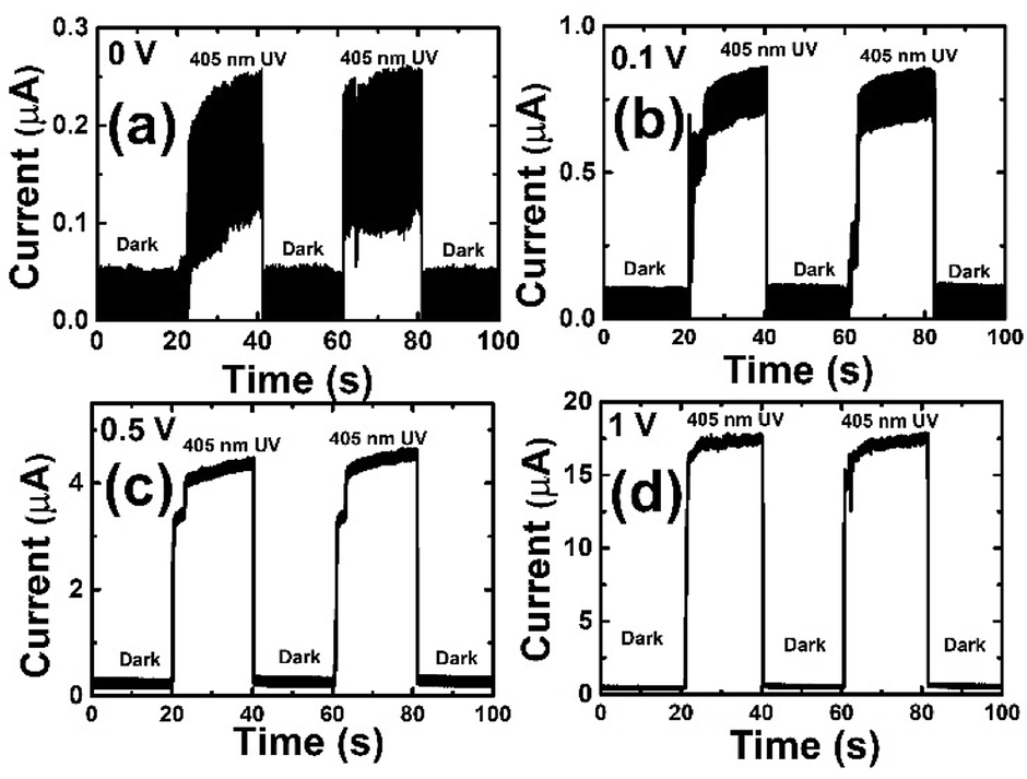 | ||
| Fig. 3 Show I–t plots for photo-detector device in dark vs. UV laser illumination. (a) and (b) are current response of the photo-detector device at the applied voltage of 0 V & 0.1 V, (c) and (d) at 0.5 V & 1 V. | ||
The working mechanism of the GaN nanorods demonstrated in this report was studied and the respective energy band diagram for the proposed model has been given in Fig. 4. The grown GaN nanorods are under the sputtered semi-transparent Au capping which enhances the nanorods' surface utilization. The energy band diagram shows that Au/GaN nanorods interface forms a potential barrier of nearly 1 eV (a Schottky barrier). Here, the photocurrents in the nanorods are attributed to the transfer of the photo-generated carriers even without applying the bias voltage. Since the work function of the Au (∼5.1 eV) is larger than that of GaN nanorods (∼4.1 eV), the Fermi energy level reaches the equilibrium and eventually forms a potential barrier at the Au/GaN interface.29 When the Au/GaN interface is illuminated with an UV laser (405 nm), a large number of photo-generated electron–hole pairs are generated. Additionally, the employment of the noble metal electrode like Au or Pt, the Au nanoparticles are possibly able to trap incident light and induce localized surface plasmon resonance (LSPR) effect.
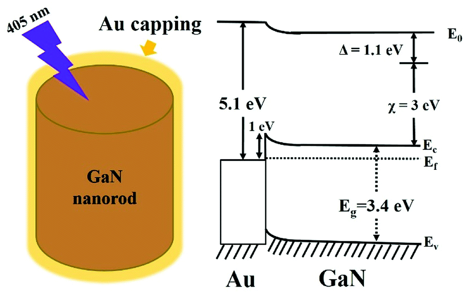 | ||
| Fig. 4 Depicts the energy band situation for the Au/GaN nanorods interface where the near-UV laser incidents. The left side image shows the nanorods' capping with the semi-transparent Au electrode. | ||
The impedance spectroscopy technique further analyzes the charge transport mechanism. In this measurement, for the dark and illuminated condition, frequency dependent parameters such as the impedance, capacitance, phase angle and tangent loss were recorded for the frequency range of 100 Hz to 1 MHz. The responses of aforementioned parameters w.r.t. frequency have been shown in Fig. 5(a–d). Fig. 5(a) shows the impedance decrement when the top surface of the GaN thin film is illuminated by the UV light source. Similarly, the capacitance and tangent loss show an increment, indicating a change in the conductivity when illuminated by the UV source. It is interesting to note that the phase angle drastically changes with an increase in probe frequency. An ideal capacitor at low frequencies shows an open circuit, so no current flows through the device and hence phase angle is nearly (−90). However, in the present case, at low frequency (∼100 Hz) the device shows the phase angle in the range of (−10) which approaches to (−70) with an increase in frequency, a situation opposite to normal capacitor, hence under direct current bias voltage it shows negative capacitance. These effects may be due to the screening of photogenerated charge carriers in the forest of GaN nanorods which originate novel properties, i.e., inbuilt OCV, SCC & NC effects.
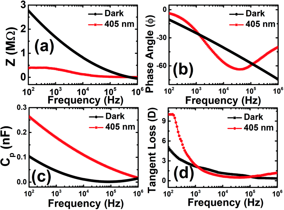 | ||
| Fig. 5 Shows the frequency vs. (a) impedance, (b) phase angle, (c) capacitance and (d) tangent loss plots for the device. | ||
Conclusions
In summary, a high-quality epitaxial GaN nanorods network has grown on N:GaN/N:HfO2/SiO2 substrate.34 The insertion of the intermediate nitride and HfO2 layers conduces favorable condition for the growth of GaN nanorods network and also acts as a barrier layer for the excess oxygen ions migration in GaN nanorods network and block the photocurrent from bottom electrode. The nanorods network shows an enhanced UV photodetection behavior with an ON/OFF resistance ratio ∼50 without any bias voltage; thus proving itself as a promising candidate for self-powered UV photodetector devices. The device shows bulk photovoltaic effects with large OCV ∼155 mV and SCC ∼430 nA similar to polar photo-ferroelectric devices. However, the response time of the GaN nanorods network was several order higher in the range of 100 ms compared to bulk photovoltaic devices and detectors (seconds per milliseconds).41–45 The capacitance characteristics of the nanorods network demonstrate the presence of NC, a suitable candidate for metamaterials.Conflicts of interest
There are no conflicts to declare.Acknowledgements
Atul Thakre would like to acknowledge the CSIR (GATE-JRF) to provide fellowship for carrying out PhD program. Authors would like to acknowledge Director, CSIR-National Physical Laboratory, New Delhi for providing essential infrastructure and facilities & Dr G. Gupta for photoluminescence measurement.References
- S. Nakamura, Science, 1998, 281, 956–961 CrossRef.
- K. Chung, C.-H. Lee and G.-C. Yi, Science, 2010, 330, 655–657 CrossRef PubMed.
- H. Wu, Y. Sun, D. Lin, R. Zhang, C. Zhang and W. Pan, Adv. Mater., 2009, 21, 227–231 CrossRef.
- B. J. Baliga, Semicond. Sci. Technol., 2013, 28, 074011 CrossRef.
- N. Ikeda, J. Li, S. Kato, M. Masuda and S. Yoshida, Furukawa Rev., 2006, 29, 1–6 Search PubMed.
- T. J. Flack, B. N. Pushpakaran and S. B. Bayne, J. Electron. Mater., 2016, 45, 2673–2682 CrossRef.
- R. D. Dupuis and M. R. Krames, J. Lightwave Technol., 2008, 26, 1154–1171 Search PubMed.
- S. T. Sheppard, K. Doverspike, W. L. Pribble, S. T. Allen, J. W. Palmour, L. T. Kehias and T. J. Jenkins, IEEE Electron Device Lett., 1999, 20, 161–163 Search PubMed.
- T. Lu, T. Kao, S. Chen, C. Kao, H. Kuo and S. Wang, in 2008 Conference on Lasers and Electro-Optics, IEEE, 2008, pp. 1–2 Search PubMed.
- S. D. Hersee, X. Sun and X. Wang, Nano Lett., 2006, 6, 1808–1811 CrossRef PubMed.
- W.-C. Hou, T.-H. Wu, W.-C. Tang and F. C.-N. Hong, Nanoscale Res. Lett., 2012, 7, 373 CrossRef PubMed.
- J. Goldberger, R. R. He, Y. F. Zhang, S. W. Lee, H. Q. Yan, H. J. Choi and P. D. Yang, Nature, 2003, 422, 599–602 CrossRef PubMed.
- S. W. Kim, Y. H. Park, I. Kim, T.-E. Park, B. W. Kwon, W. K. Choi and H.-J. Choi, Nanoscale, 2013, 5, 8550 RSC.
- D. Poppitz, A. Lotnyk, J. W. Gerlach and B. Rauschenbach, Acta Mater., 2014, 65, 98–105 CrossRef.
- S. Jiang, J. Zhang, X. Qi, M. He and J. Li, CrystEngComm, 2013, 15, 9837 RSC.
- H. S. Jung, Y. J. Hong, Y. Li, J. Cho, Y. J. Kim and G. C. Yi, ACS Nano, 2008, 2, 637–642 CrossRef PubMed.
- J. Y. Huang, H. Zheng, S. X. Mao, Q. Li and G. T. Wang, Nano Lett., 2011, 11, 1618–1622 CrossRef PubMed.
- S. J. Pearton, B. S. Kang, B. P. Gila, D. P. Norton, O. Kryliouk, F. Ren, Y. Heo, C. Chang, G. Chi, W. Wang and L. Chen, J. Nanosci. Nanotechnol., 2008, 8, 99–110 CrossRef PubMed.
- C.-H. Lin and C. W. Liu, Sensors, 2010, 10, 8797–8826 CrossRef PubMed.
- E. Monroy, F. Omn s and F. Calle, Semicond. Sci. Technol., 2003, 18, R33–R51 CrossRef.
- F. Omnès, E. Monroy, E. Muñoz and J.-L. Reverchon, International Society for Optics and Photonics, ed H. Morkoc and C. W. Litton, 2007, vol. 6473 Search PubMed.
- M. Razeghi and A. Rogalski, J. Appl. Phys., 1996, 79, 7433–7473 CrossRef.
- E. Muñoz, Phys. Status Solidi B, 2007, 244, 2859–2877 CrossRef.
- T. Zhai, X. Fang, M. Liao, X. Xu, H. Zeng, B. Yoshio and D. Golberg, Sensors, 2009, 9, 6504–6529 CrossRef PubMed.
- C. Soci, A. Zhang, B. Xiang, S. A. Dayeh, D. P. R. Aplin, J. Park, X. Y. Bao, Y. H. Lo and D. Wang, Nano Lett., 2007, 7, 1003–1009 CrossRef PubMed.
- Q. Yang, X. Guo, W. Wang, Y. Zhang, S. Xu, D. H. Lien and Z. L. Wang, ACS Nano, 2010, 4, 6285–6291 CrossRef PubMed.
- L. Rigutti, M. Tchernycheva, A. De Luna Bugallo, G. Jacopin, F. H. Julien, L. F. Zagonel, K. March, O. Stephan, M. Kociak and R. Songmuang, Nano Lett., 2010, 10, 2939–2943 CrossRef PubMed.
- M. H. Huang, Science, 2001, 292, 1897–1899 CrossRef PubMed.
- X. Zhang, Q. Liu, B. Liu, W. Yang, J. Li, P. Niu and X. Jiang, J. Mater. Chem. C, 2017, 5, 4319–4326 RSC.
- R. Yu, C. Pan, Y. Hu, L. Li, H. Liu, W. Liu, S. Chua, D. Chi and Z. L. Wang, Nano Res., 2013, 6, 758–766 CrossRef.
- D. Li, X. Sun, H. Song, Z. Li, Y. Chen, H. Jiang and G. Miao, Adv. Mater., 2012, 24, 845–849 CrossRef PubMed.
- J. Miao, W. Hu, Y. Jing, W. Luo, L. Liao, A. Pan, S. Wu, J. Cheng, X. Chen and W. Lu, Small, 2015, 11, 2392–2398 CrossRef PubMed.
- Z. Jin, L. Gao, Q. Zhou and J. Wang, Sci. Rep., 2015, 4, 4268 CrossRef PubMed.
- C. Ramesh, P. Tyagi, P. Singh, A. Kumar, M. Senthil Kumar and S. S. Kushvaha, Mater. Res. Express, 2018, 5, 095902 CrossRef.
- K. Shubhakar, K. L. Pey, N. Raghavan, S. S. Kushvaha, M. Bosman, Z. Wang and S. J. O'Shea, Microelectron. Eng., 2013, 109, 364–369 CrossRef.
- S. S. Kushvaha, M. S. Kumar, A. K. Shukla, B. S. Yadav, D. K. Singh, M. Jewariya, S. R. Ragam and K. K. Maurya, RSC Adv., 2015, 5, 87818–87830 RSC.
- H. Borkar, A. Thakre, S. S. Kushvaha, R. P. Aloysius and A. Kumar, RSC Adv., 2015, 5, 35046–35051 RSC.
- H. Zhou, P. Gui, Q. Yu, J. Mei, H. Wang and G. Fang, J. Mater. Chem. C, 2015, 3, 990–994 RSC.
- H. Borkar, V. Rao, M. Tomar, V. Gupta, J. F. Scott and A. Kumar, RSC Adv., 2017, 7, 12842–12855 RSC.
- L.-F. Feng, K. Zhao, H.-T. Dai, S.-G. Wang and X.-W. Sun, Chin. Phys. B, 2016, 25, 037307 CrossRef.
- L. Zheng, K. Hu, F. Teng and X. Fang, Small, 2017, 13, 1602448 CrossRef PubMed.
- M. Ahmadi, T. Wu and B. Hu, Adv. Mater., 2017, 29, 1605242 CrossRef PubMed.
- Q. Wang, J. Lai and D. Sun, Opt. Mater. Express, 2016, 6, 2313 CrossRef.
- A. Anshul, H. Borkar, P. Singh, P. Pal, S. S. Kushvaha and A. Kumar, Appl. Phys. Lett., 2014, 104, 132910 CrossRef.
- C. Paillard, X. Bai, I. C. Infante, M. Guennou, G. Geneste, M. Alexe, J. Kreisel and B. Dkhil, Adv. Mater., 2016, 28, 5153–5168 CrossRef PubMed.
| This journal is © The Royal Society of Chemistry 2018 |