DOI:
10.1039/C8RA05662E
(Paper)
RSC Adv., 2018,
8, 31055-31065
Copper antimony sulfide thin films for visible to near infrared photodetector applications†
Received
2nd July 2018
, Accepted 22nd August 2018
First published on 4th September 2018
Abstract
Ternary chalcostibite copper antimony sulfide (CuSbS2) is an emerging semiconductor material having applications in photovoltaics, energy storage and optoelectronics due to its high absorption coefficient, suitable bandgap, and it consists of non-toxic and earth abundant elements. CuSbS2 thin films are prepared by combining chemical bath deposition (antimony sulfide (Sb2S3)) and thermal evaporation (copper (Cu)) followed by a heat treatment and their application as visible to near infrared photodetectors is reported. Crystalline structure, elemental composition, chemical state, morphology and optoelectronic properties of the films were characterized by various techniques. The effect of three different Cu thicknesses (CAS 20, CAS 30 and CAS 40 nm) on the photodetection properties are evaluated under illumination using light emitting diodes (LEDs) and a laser. The photodetectors fabricated are successfully tested under different wavelengths, power densities and applied voltage and their photoresponse cyclic stability for each wavelength of illumination was recorded. From the sensitivity calculations, the sample with 20 nm Cu thickness (CAS 20) showed higher detection sensitivity for visible to near infrared wavelengths. Better responsivity results were obtained for CAS 40 because of its improved crystallinity and phase purity. Photodetector properties such as sensitivity and responsivity are evaluated for all the samples. These results are beneficial for cost effective and environment friendly photodetectors and optoelectronic devices based on CuSbS2 thin films.
1. Introduction
Semiconductor nanocrystals have played major roles in developing novel and efficient electronic and optical devices.1 Among these, ternary and quaternary chalcogenide systems such as copper indium sulfide (CuInS2), copper indium selenide (CuInSe2) and copper indium gallium selenide (CIGS) possess bulk band gaps appropriate for solar light harvesting.2 Even though most researchers focused on exploring photovoltaic properties of these chalcogenides, they exhibit reliable opto-electronic properties as well. Based on this hypothesis, high performance photo detecting devices were fabricated using the chalcogenides as the active material. Wang et al. used monodispersed CuInSe2 to fabricate a hybrid photodetector of high sensitivity and stability.3 A flexible photodetector was fabricated using aluminum doped zinc oxide (Al:ZnO) and CIGS nanorods where the improved photocurrent was attributed to the light trapping properties and core shell structure of CIGS.4 However, indium (In) in these chalcogenide materials is expensive due to its scarcity. Antimony (Sb) is the best substitute for In due to its similar chemistry, thus forming CuSbS2.5,6
Copper antimony sulfide (CuSbS2 or CAS) is a newly emerging p-type semiconductor, which has attracted much attention due to its versatile properties, environmentally benign and earth abundant precursor materials and cost consideration.5,7–10 So far, the focus of researchers has been in exploring the photovoltaic properties of CuSbS2 as an absorbing layer due to its appropriate bandgap of 1.5 eV![[thin space (1/6-em)]](https://www.rsc.org/images/entities/char_2009.gif) 11,12 (optimum for photovoltaic solar energy conversion), a high absorption coefficient ∼ 105 cm−1,12–15 tunable hole concentration in a range of 1016–1018 cm−1,16,17 hole mobility of 49 cm2 (V s)−1, grain growth at relatively low temperatures and the Spectroscopic Limited Maximum Efficiency (SLME) of 22.9%.13,18,19 Additionally, interesting optoelectronic properties, especially in the visible-near infrared (NIR) region, for CuSbS2 can make it an inventive candidate in optoelectronic devices. Hao et al. reported the synthesis of CuSbS2 nanocrystals using a hot injection method and fabrication of a high performance hybrid photodetector based on a poly(3-hexylthiophene):CuSbS2 hybrid films6 where, the CuSbS2 acted as a photoelectron accepter due to its high electron affinity. Application of CuSbS2 as an anode material in charge storage devices was also explored by the research community.20–22
11,12 (optimum for photovoltaic solar energy conversion), a high absorption coefficient ∼ 105 cm−1,12–15 tunable hole concentration in a range of 1016–1018 cm−1,16,17 hole mobility of 49 cm2 (V s)−1, grain growth at relatively low temperatures and the Spectroscopic Limited Maximum Efficiency (SLME) of 22.9%.13,18,19 Additionally, interesting optoelectronic properties, especially in the visible-near infrared (NIR) region, for CuSbS2 can make it an inventive candidate in optoelectronic devices. Hao et al. reported the synthesis of CuSbS2 nanocrystals using a hot injection method and fabrication of a high performance hybrid photodetector based on a poly(3-hexylthiophene):CuSbS2 hybrid films6 where, the CuSbS2 acted as a photoelectron accepter due to its high electron affinity. Application of CuSbS2 as an anode material in charge storage devices was also explored by the research community.20–22
Thin films of CuSbS2 have been fabricated using various chemical and physical methods such as chemical bath deposition,23 spray pyrolysis,24 spin coating,9 electro deposition,25 thermal evaporation26 and co-sputtering.5 Chemical bath deposition (CBD) is a relatively less expensive thin film fabrication technique due to the absence of sophisticated instrumentation and vacuum system. Use of non-conductive substrates, large area and uniform deposition are other advantages of CBD.27,28 Thermal evaporation on the other hand acquires uniform thin films by heating the target material and condensing on the substrate. Pre-defined thin film thickness with accuracy in the nanometer range is one of the major advantages of thermal evaporation technique. Garza et al. fabricated CuSbS2 thin films by combined chemical bath and thermal evaporation techniques followed by a heat treatment.8 Furthermore, we have reported the successful fabrication of single phase CuSbS2 thin films by a rapid thermal processing (RTP) applied to glass/Sb2S3/Cu stacked layer pre-annealed in a vacuum system.29
In this work, we report the fabrication of CuSbS2 thin films on glass substrates for photodetection application. Thin films of Sb2S3 and Cu (thicknesses of 20, 30 and 40 nm) were deposited on glass substrates by chemical bath deposition followed by thermal evaporation technique. CuSbS2 thin films were obtained by a heat treatment in vacuum oven for Sb2S3/Cu precursors at 380 °C. CAS thin films synthesized were characterized using various techniques such as X-ray diffraction (XRD), Raman spectroscopy, X-ray photoelectron spectroscopy (XPS), scanning electron microscopy (SEM), atomic force microscopy (AFM), UV-Vis NIR spectroscopy and an electrical measurement system. Photodetector properties were investigated using LED lights of different wavelength illuminations, applied voltages and laser power densities. The photodetector with 40 and 30 nm Cu thickness showed better photodetector characteristics in the visible region where as the one with 20 nm showed better NIR response. The details of the characterization of CAS thin films and their photodetector properties are described. The results show that the CAS thin films are of good visible to NIR light response at low applied voltages (1, 3 and 5 V), linear photocurrent response with stable and reproducible photodetection properties.
2. Experimental procedure
2.1. Materials
Neutral soap solution, isopropyl alcohol, antimony trichloride (SbCl3-99.999%) powder, sodium thiosulfate pentahydrate (Na2S2O3·5H20-99.999%) powder and acetone were supplied by Fermont. All the chemicals were used as received. Copper wire (Cu-99.999%) was purchased from Alpha Aesar.
2.2. Preparation of CuSbS2 thin film
Chemical bath deposition (CBD) technique was employed to deposit thin films of antimony sulfide (Sb2S3) on glass substrates30 from a bath containing 650 mg of antimony trichloride (SbCl3) dissolved in 2.5 ml of acetone, 25 ml of sodium thiosulfate pentahydrate (Na2S2O3·5H2O) having concentration of 1 M and 72.5 ml of deionized water (25 °C).29 The whole mixture was stirred well and poured slowly into Petri dish without making bubbles where the well cleaned glass substrates (ultrasonically cleaned with isopropanol, neutral soap solution and distilled water) were placed horizontally. The deposition was carried out at 25 °C for 2 hours. Afterwards, the substrates with thin films were removed from the Petri dish and rinsed with distilled water and dried using hot air. As prepared Sb2S3 films were orange-yellow in color and uniformly reflective.
Copper layers of thicknesses 20, 30 and 40 nm were deposited on Sb2S3 thin films coated glass substrates by thermal evaporation of copper in a high vacuum system (Torr International, Model No: THE2-2.5KW-TP) at a pressure of 10−6 torr with a rate of 1 Å s−1 and substrate rotation of 20 rpm. 99.999% pure copper wire was used as the evaporation material. Thickness of the Cu film was measured in situ using a quartz crystal thickness monitor installed in the evaporation system. Copper antimony sulfide (CuSbS2 (CAS)) phase was formed by annealing glass/Sb2S3/Cu precursor layers with different Cu thicknesses in a vacuum oven (10−3 torr) at 380 °C for 1 hour. Samples annealed were labelled as CAS 20, CAS 30 and CAS 40 depending on the thickness of the Cu layer (in nm) deposited on Sb2S3 thin films.
2.3. Characterization
The structural properties of CuSbS2 thin films were characterized by X-ray diffraction technique (PANalytical Empyrean Diffractometer which employs Cu Kα1 radiation (λ = 1.54056 Å)) in the range of 2θ = 10–60°. Raman spectroscopy (Thermo Scientific DXR Raman Microscope) was used to identify the phases present in these CAS thin films. The elemental composition and chemical states were analysed by X-ray photoelectron spectroscopy (XPS, Thermo Scientific K-Alpha) with a monochromatized Al Kα radiation (hν = 1486.88 eV). Scanning electron microscopy (SEM, Hitachi Model SU 8020) and atomic force microscopy (AFM, NT-MDT Model Solver Pro) were used to characterize the morphology as well as surface roughness of the films. Optical spectral measurements were carried out using an ultraviolet-visible-near infrared spectrophotometer (Jasco V770). Transmittance as well as absorbance measurements were done by keeping a bare glass substrate as reference in the wavelength range of 400 to 1000 nm. The optical energy bandgap (Eg) values were evaluated using Tauc plot between (αhν)2 vs. hν for all the films. Electrical properties as well as photoresponse measurements were carried out under the illumination from light emitting diodes (LEDs) having wavelengths of 450, 620, 740 and 850 nm and optical power of 20 W using a picoammeter/voltage source meter (Keithley 6487). A pair of silver electrodes of 5 mm in length separated by 5 mm were painted using conductive silver paint (SPI® supplies) and dried on the sample surface for the photodetector characterization. The current voltage measurements were carried out under dark as well as illumination for applied voltages from −5 to +5 V. Photoresponse switching behaviour of the CuSbS2 thin films were measured at different applied potentials of 1, 3 and 5 V where the LED illumination was turned on and off at each 5th and 10th seconds respectively.
Photodetection properties of CAS thin films for various intensities were measured by illuminating the samples using a diode pumped continuous wave laser of 532 nm with adjustable output power. The laser spot was expanded using a concave lens and the sample area excess of the electrode dimension was masked to avoid illumination. The same voltage source (Keithley 6487) used to apply voltage and simultaneously to measure current while the samples were illuminated by the laser. Laser output power was varied from 2 mW to 40 mW (2, 6, 10, 20, 30, and 40 mWs) during constant bias voltages 1, 3 and 5 V and photoresponse was measured for 20 s in dark, 20 s in light followed by another 20 s in dark.
3. Results and discussion
3.1. Structural analysis
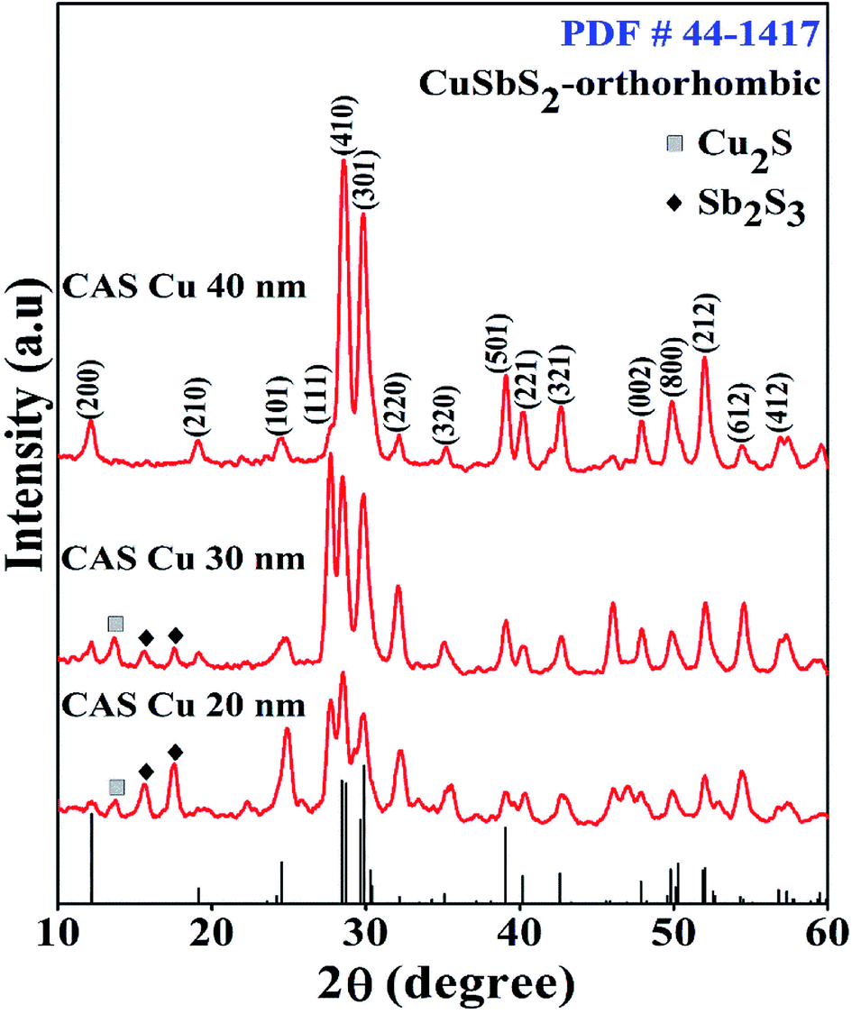
X-ray diffraction at grazing incidence mode was carried out for these CAS thin films for their structural characterization. Copper thicknesses of 20, 30 and 40 nm were selected to optimize the photoconductive properties of the CAS thin films. Structural characterization of CAS 20, CAS 30 and CAS 40 thin films annealed at 380 °C for 1 h is shown in Fig. 1. The diffraction patterns were collected at 0.5° incident angle in grazing incident mode for all the samples. The major reflections observed in XRD are from the planes (200), (101), (111), (410), (301), (501), (221), (321), (002), (800), and (212) that correspond to the orthorhombic crystal structure of CuSbS2 (JCPD#44-1417). These XRD peaks are matching well with the reported results.9,11,31,32 Nair et al. reported the formation of ternary CuSbS2 films by annealing chemically deposited multilayer thin films7,31 and Yang et al. by spin coating followed by a hot plate heat treatment.9 In both studies, the major XRD reflections are from the same planes as we observed in the present work. Phase pure CuSbS2 peaks with improved crystalline nature was observed for the CAS 40 nm film from the diffraction pattern analysis. The intensity of the peak corresponds to the plane (111) is diminished whereas more orientations are noted along (410), (301), (501) and (212) planes. JCPDS reference data for orthorhombic CuSbS2 is also provided in Fig. 1. All the peaks in the reference JCPDS are identified in the CAS 40 thin film. For CAS 20 and CAS 30 films, reflections from the planes (020) and (120) correspond to Sb2S3 for the stibnite crystal structure (JCPDS#42-1393). This could be attributed to the deficiency of Cu in the CAS 20 and CAS 30 thin films to form the complete ternary CAS phase. A feeble amount of Cu2S impurity is also identified at 2θ value 13.8 in these samples irrespective of the Cu thicknesses (chalcostibite, JCPDS#83-1462). The presence of impurity Cu2S peak at the same 2θ value was reported by Aquino et al.33 and Acosta et al.11 where, the films were prepared by spray pyrolysis and combined chemical bath and thermal evaporation techniques. Colombara et al. reported the sulfurization of Sb–Cu metal precursors at different temperatures which resulted in the formation of CuSbS2 films with a minor presence of binary CuS phase.34 These studies report the binary impurity phases (CuS and Cu2S) formation during the synthesis of ternary CuSbS2 phase. However, as the Cu thickness increased from 20 to 30 nm, the intensity of peaks corresponding to CuSbS2 also increased significantly while diminishing the Sb2S3 peak intensities. The average crystallite sizes of all the CAS films with different Cu thicknesses were evaluated using Scherrer equation,29,35| |
 | (1) |
where, λ is the wavelength of the X-ray radiation (1.54056 Å), θ is the Bragg angle and β is the full width at the half maximum (FWHM) of the (410) peak. The crystalline size estimated from the Scherrer equation are 13, 13.6 and 14.6 nm for the CAS 20, CAS 30 and CAS 40 samples respectively where the crystalline size increased with the increase in the Cu layer thickness. All these results are comparable with previously reported results.29
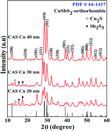 |
| | Fig. 1 XRD pattern of CuSbS2 thin films with varying Cu thicknesses 20, 30 and 40 nm annealed at 380 °C for 1 h in vacuum oven. The standard pattern corresponding to orthorhombic CuSbS2 is included (PDF#44-1417). | |
3.2. Raman analysis
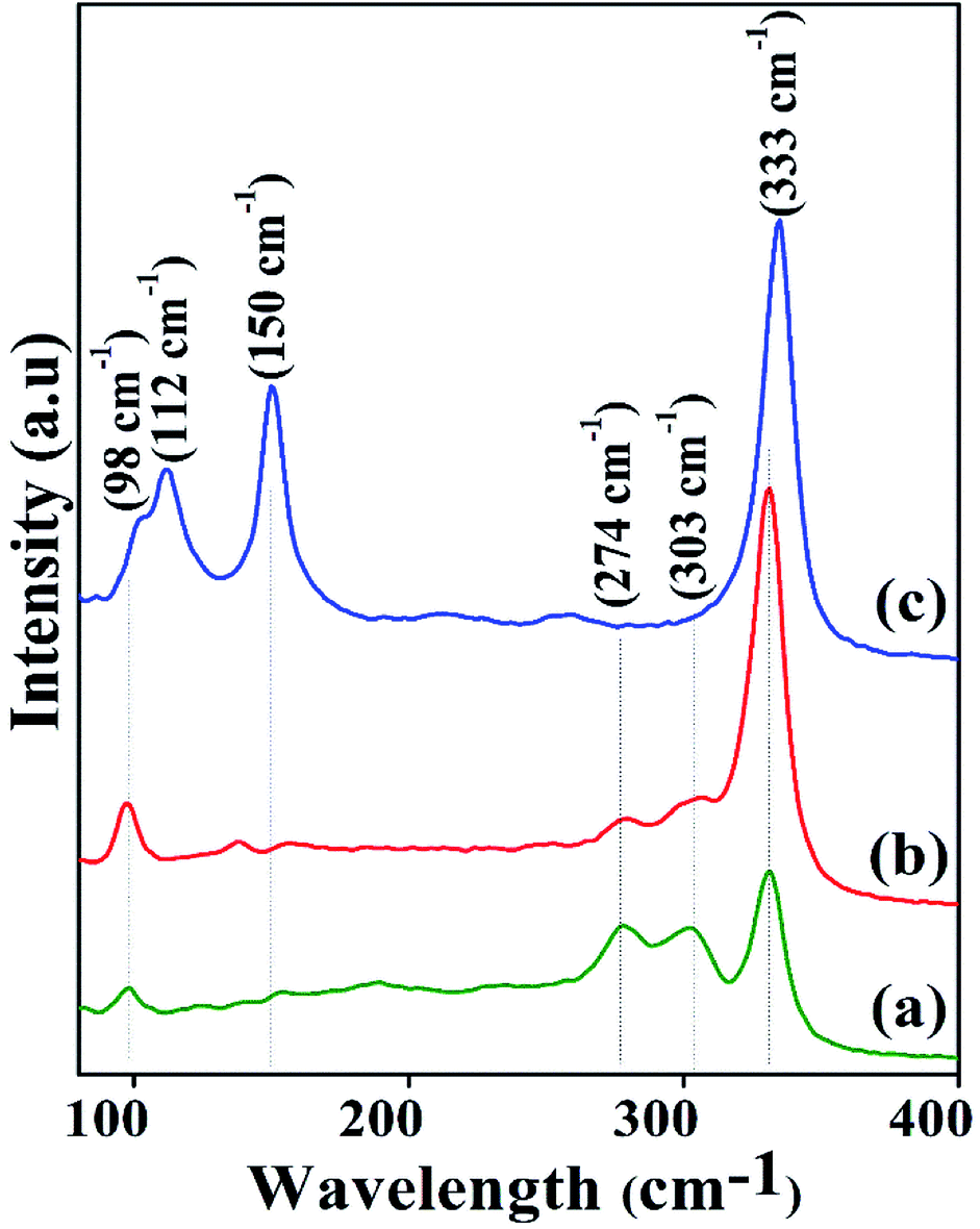
Fig. 2 shows the Raman spectra using 532 nm laser excitation for identification of crystalline phases present in the films. As specified by Baker et al.,36 CuSbS2 possess four Raman active modes represented by Ag, B1g, B2g and B3g and three infrared active modes B1u, B2u and B3u. The present spectra shows Raman bands at 98, 112, 150, 274, 303 and 333 cm−1 where the peaks at 98, 112, 150 and 333 cm−1 are attributed to the vibrational modes of CAS33,36–39 and the peaks at 274 and 303 cm−1 correspond to the Sb2S3 phase.40,41 Raman peak values obtained for the samples are in good agreement with the reported Raman active vibrations of CAS and Sb2S3. Raman intensity of the CAS peak at 333 cm−1 is increased significantly as Cu thickness raised from 20 to 40 nm which is in good agreement with the XRD results. As seen in the figure, presence of precursor Sb2S3 is noted in the CAS films with Cu thickness 20 nm and minor traces in 30 nm. However, the intensities of the peaks corresponding to Sb2S3 (274 and 303 cm−1) are decreasing gradually with increase in Cu thickness. It can be inferred from the Raman spectra that both these films contain CAS as the major phase along with small contribution from the unreacted Sb2S3 phase. CAS 40 nm film shows two additional peaks at 112 and 150 cm−1 along with the major peak at 333 cm−1 which also corresponds to the CuSbS2 phase. These peaks are also identical with the RRUFF project data base of the Raman spectra of CuSbS2 sample at 532 nm excitation wavelength42 as well as with our previous reports.29,33 Raman results indicate the phase purity for CuSbS2 thin films formed for 40 nm Cu thickness (CAS 40). Results of the Raman spectra for CAS samples are in accordance with the XRD results obtained.
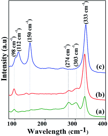 |
| | Fig. 2 Raman spectra of CAS thin films with varying Cu thicknesses (a) 20, (b) 30 and (c) 40 nm annealed at 380 °C for 1 hour in vacuum oven. | |
3.3. X-ray photoelectron spectroscopy (XPS)
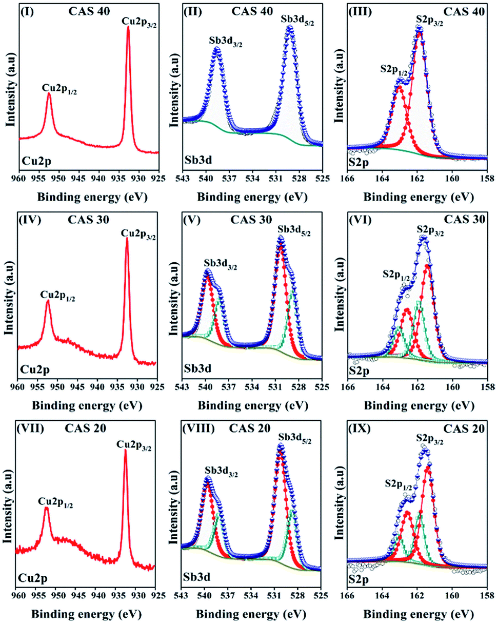
X-ray photoelectron spectroscopy was employed to determine the elemental composition and chemical states using a typical survey and high resolution spectral analyses of the CAS thin films. Low resolution survey spectra recorded from 0 to 1400 eV were used for the elemental analysis of each sample (provided in ESI, Fig. S1†) whereas high resolution spectra of Cu, Sb and S were used for the chemical states analysis. Fig. 3 shows the high-resolution photoelectron spectra of Cu, Sb and S of CAS 20, 30 and 40 from the first etch level where etching cycles were performed at a rate of 1.19 nm s−1 using 2 keV Ar+ ions to remove the surface contaminants. A Shirley type background and a Gaussian–Lorentzian sum function were applied to the XPS high resolution spectra for deconvolution of the peaks, as shown in the figure. Fig. 3(I–III) presents the high-resolution scans of Cu2p, Sb3d and S2p core level spectra of CAS 40 thin film where, copper core level spectrum shows a 2p doublet at the binding energies (B.E) 932.6 eV and 952.3 eV with a separation of 19.7 eV, which is consistent with previous reports for Cu2+ in CuSbS2. XPS analysis of CuSbS2 thin films by solution processing and spin coating were reported by Yang et al. and McCarthy et al. observed the similar B.E for Cu2p peaks.9,37 The 3d core level spectra of antimony observed at 530.43 eV (3d5/2) and 539.82 eV (3d3/2) with a separation of 9.39 eV match with CuSbS2 phase as reported earlier.29 The high-resolution core level spectra of S2p doublet is shown in Fig. 3(III). Deconvoluted high intensity peaks located at 161.7 (2p3/2) and 162.9 (2p5/2) eV coincide with the reported B.E values of CuSbS2.
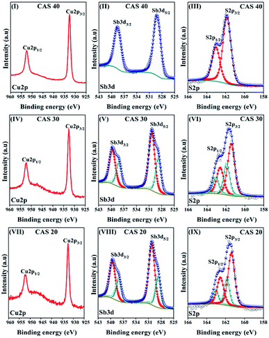 |
| | Fig. 3 High resolution spectra of Cu2p, Sb3d and S2p of CAS 40 (I–III), CAS 30 (IV–V) and CAS 20 (VI–IX) thin films. | |
Fig. 3(IV–VI) and (VII–IX) represent the high-resolution spectra of CAS 30 and CAS 20 thin films respectively. They both present similar binding energy peaks as CAS 40 nm with an extra peak in S2p and Sb3d core levels. The smallest peak observed in S2p and Sb3d at 161.8 eV (S2p3/2), 163 eV (S2p1/2) with a separation of 1.2 eV and 528.8 eV (Sb3d5/2), 538.19 eV the Sb2S3 phase is highly intense in the CAS 30 and CAS 20 samples due to the presence of unreacted Sb2S3 owing to the insufficient Cu thickness for complete CAS formation. The uniformity of Cu, Sb and S elements throughout the depth of the films were observed in the depth profile analysis of each sample, one of them is included in the ESI (Fig. S2†). All these XPS results agree with that of XRD and Raman analysis.
3.4. Morphological studies
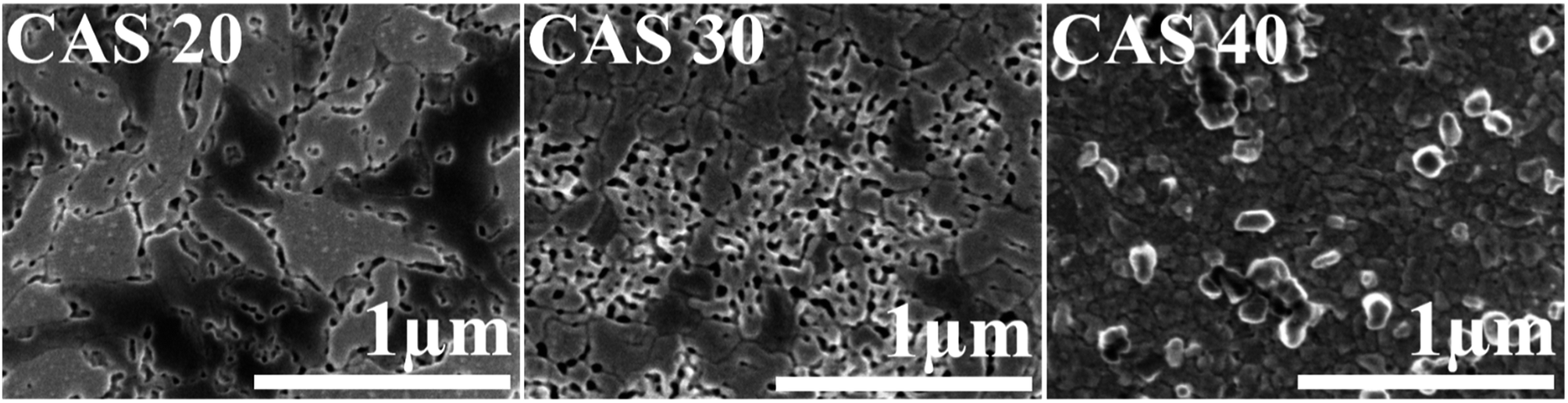
The morphology and surface roughness of the CAS thin films were analysed using SEM and AFM. Field emission scanning electron microscopic (FESEM) images of the annealed CAS thin films with varying Cu thicknesses are in Fig. 4. Images were collected in secondary electron imaging mode by applying 1 kV at the same magnification (50000×). All films show changes in as Cu thickness increases from 20 to 40 nm. The CAS 20 film exhibits irregular shaped particles interconnected as seen in the figure. In the CAS 30 film, a compact morphology with better grains is observed. Pinhole free films with bigger grains with definite boundaries are formed when Cu thickness is increased to 40 nm. These morphological analyses are consistent with our previous reports.8,11,29 The thickness of the films was measured by cross-sectional SEM analysis (images are provided in the ESI, Fig. S3†). The EDX spectrum taken from the samples reveals the peaks of Cu, Sb and S as well as EDX mapping provide the information about the spatial distribution of different compositional elements of CuSbS2 (Fig. S4 and S5†).
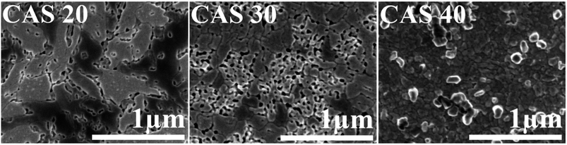 |
| | Fig. 4 Scanning electron micrographs for CuSbS2 thin films with 20 (CAS 20), 30 (CAS 30) and 40 nm (CAS 40) Cu thicknesses. | |
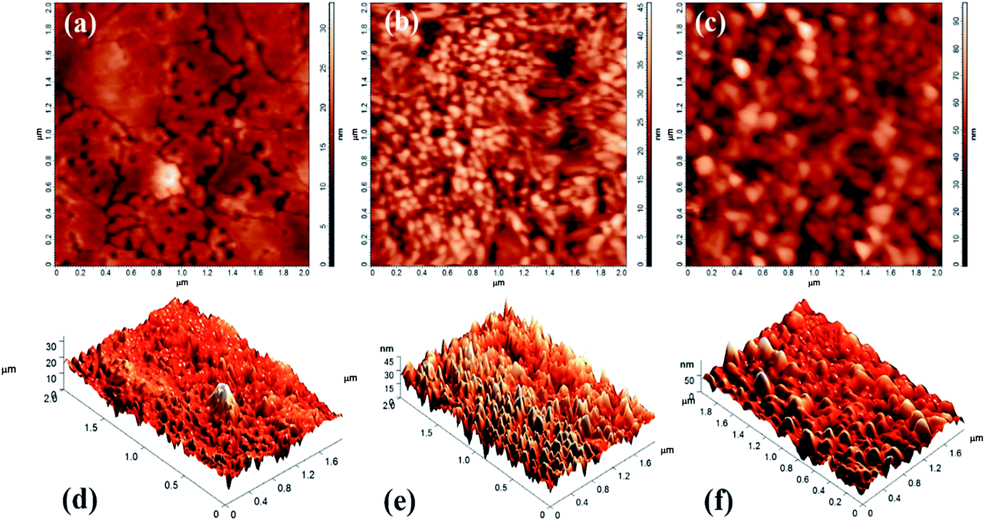
The surface morphology and roughness of all CAS films were investigated by atomic force microscopy (AFM) in contact mode. Fig. 5(a–c) and (d–f) show the 2D as well as 3D AFM images of CAS thin films CAS 20, CAS 30 and CAS 40 respectively. From the figure, grain size and roughness of the films are increasing gradually with the increase in Cu thickness from 20 to 40 nm. AFM images are taken by scanning an area of 2 × 2 μm. Roughness of the film surfaces calculated are 2.99 nm, 6.36 nm and 11.34 nm respectively for CAS 20, 30 and 40. Surface of the films appears as flat for the CAS 20 compared to other two whereas small grains appear in CAS 30 film. For CAS 40 much bigger spherical grains are identified. Change in morphology of the films with varying Cu thickness is evident from SEM and AFM images. In both cases CAS 40 film showed better surface morphology which is in good agreement with the XRD results having higher crystallinity.
 |
| | Fig. 5 Atomic force micrographs (2D) for CuSbS2 thin films with varying Cu thicknesses (a) CAS 20 (b) CAS 30 (c) CAS 40 and (d–f) their corresponding 3D images. | |
3.5. Optical properties
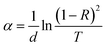
The optical absorbance and energy bandgap of the CAS thin films deposited on glass substrates were evaluated using UV-Vis-NIR spectrometer for the range of 400–1000 nm. Fig. 6 shows the absorption spectra for CAS 20, 30 and 40 films and their bandgaps (inset) respectively. A broad as well as strong absorbance in the range of 400 to 800 nm and its reduction at higher wavelength is clear from the given spectra. Optical bandgap of the films calculated using the Tauc plots based on the relation,where α is the absorption coefficient corresponding to the energy hν where h is the Plank's constant, ν is the frequency of the incident photon, and A is a constant. The value of n equals to 2 for an allowed direct, 1/2 for an allowed indirect and 2/3 for a forbidden transition. Absorption coefficient (α) in the absorbance region was calculated using the eqn (3),| |
 | (3) |
where, d is the thin film thickness (≈220, 230 and 240 for CAS 20, 30 and 40 films), R is the reflectance and T is the transmittance (graphs of T and R is provided in the ESI, Fig. S6†). A good linear fit of (αhν)2 vs. hν (Tauc plot) is obtained for n = 2 (direct-allowed transition) for all the CAS thin films which implies that in CuSbS2 films the fundamental optical absorption is dominated by direct allowed transition.11 The bandgap obtained for CAS 20, 30 and 40 films are 1.63, 1.58, 1.50 eV respectively.43 The widest bandgap observed for 20 nm CAS film might be due to the higher extent of unreacted Sb2S3 present in it. Sanchez et al. reported that the higher electron–hole pair generation and potent absorption coefficient resulted due to the direct band gap44 which is suitable for the optoelectronic device applications. Furthermore, UV to NIR spectra detection would also be possible considering this direct band gap values.45
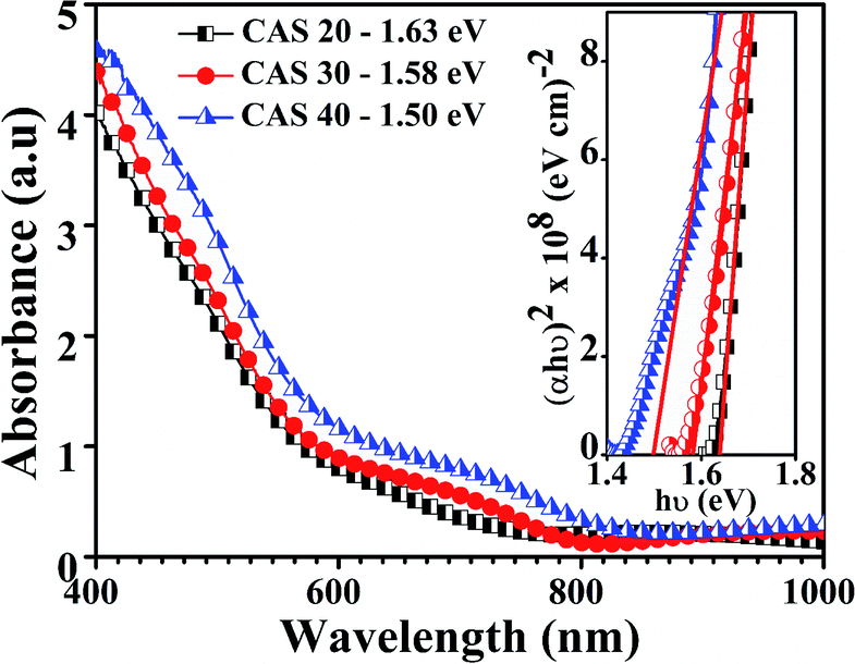 |
| | Fig. 6 Optical absorption spectra of phase pure CAS thin films with varying Cu thicknesses 20, 30, and 40 nm. Tauc plots for the evaluation of optical bandgaps are given in the inset. | |
3.6. Electrical and photodetector properties
The current–voltage (I–V) characteristics of CuSbS2 photodetector having varying Cu thicknesses under dark as well as illumination at different wavelength LEDs for an applied voltage from −5 V to +5 V is shown in Fig. 7. As shown in the figure, good symmetry and linear nature of the I–V curves for all the films suggest better ohmic contact between the Ag electrodes and CAS films. The photocurrent analysis under dark as well as light at the same bias voltage shows a significant increase in current with the illumination. The p-type conductivity and high absorption coefficient favour this material for linear and symmetrical I–V characteristics under dark and illuminated conditions. This linear and stable nature of I–V characteristics under illumination agrees with the light absorption, charge carrier generation (electron–hole) and transport leading to increase in photocurrent compared to that in dark.
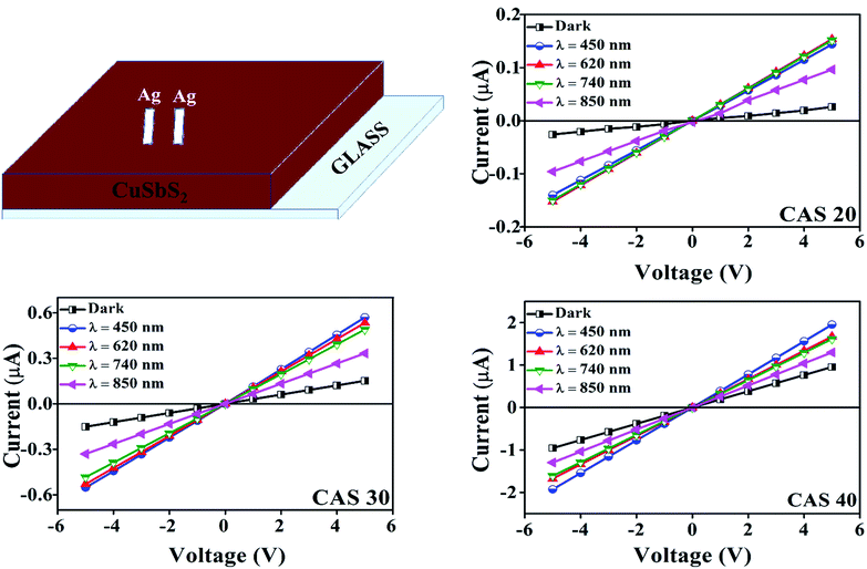 |
| | Fig. 7 Schematic representation of the CAS photodetector device, the current voltage curves of the CAS 20, 30 and 40 photodetectors under dark and illumination with different wavelength LED's (450, 620, 740 and 850 nm) light. | |
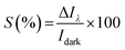
CAS 40 and CAS 30 showed the highest photocurrent for the illumination wavelength of 450 nm which coincide with the optical results where the maximum absorption was in this wavelength range. These results are comparable with the performance of flexible photodetector based on SnS thin films by Mahdi et al.45 For the SnS photodetector illuminated by LED having wavelength of 380 nm showed better photocurrent rather than the LEDs with higher wavelengths which is well matching with the current work. Photoresponse of CAS 20, CAS 30 and CAS 40 samples at 1 V (photoresponse for applied voltages of 3 and 5 V are provided in ESI, Fig. S7 and S8†) under dark as well as illumination using LEDs having wavelength of 450, 620, 740 and 850 nm at a cyclic interval of 5 s is shown in Fig. 8. As observed in the previous results, CAS 40 as well as 30 films show highest photocurrent for illumination having a wavelength of 450 nm. CAS 20 shows better photocurrent for 740 nm, which provides wavelength selective photodetection for CAS thin films. This might be due to the presence of binary impurity phases, defects present in this sample as well as the surface morphology. For all the samples, the photocurrent increased to a stable value under each bias voltage and reached back to its initial value as illumination is turned off (on/off nature of photocurrent), which shows the stability as well as reproducibility characteristics of the CAS photodetector. The cyclic photo response of the CAS films in the present work is of better stability with higher order of photocurrent (103 times) at much lower applied voltages compared to the results obtained for organic–inorganic photodetector based on CuSbS2 nanocrystals.6 The measure of change in conductivity of a sample upon illumination (photosensitivity) of the photodetectors are measured using eqn (4)45,46 from both photoresponse using LEDs as well as the laser,
| |
 | (4) |
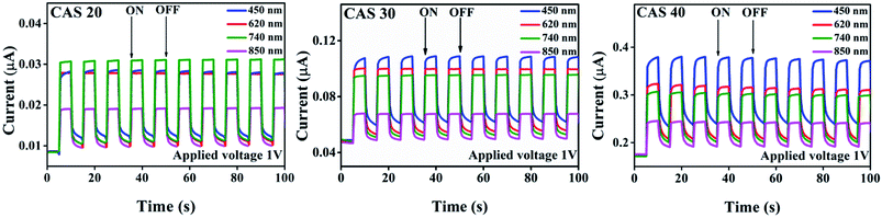 |
| | Fig. 8 Switching behaviour of CAS photodetector (CAS 20, CAS 30 and CAS 40) under illumination with LEDs having wavelengths 450, 620, 740 and 850 nm for bias voltage 1 V. | |
The corresponding results are shown in Tables 1 and 2 for the applied bias voltage 1 V (sensitivity values corresponding to applied voltages 3 V and 5 V are provided in the ESI Tables ST1–ST4†). For the measurements using different wavelength LEDs, highest sensitivity for the CAS 20 sample is obtained for 740 nm whereas CAS 30 and CAS 40 samples show highest sensitivities for blue light (450 nm). The corresponding photoresponse measurements using LEDs are shown in Fig. 8. Among all the samples, better sensitivity under all the wavelengths of illumination is recorded for CAS 20 film for all applied voltages. These results were further verified using another set of samples of CAS 20 thin films. From the analysis of structure and morphology of this sample, the presence of impurity phases as well as the different surface morphology of this sample might have contributed to this selective NIR photodetection with enhanced sensitivity.
Table 1 Sensitivity measurements of CAS 20, 30 and 40 using LEDs at applied voltage 1 V
| Sample |
Wavelength (nm) |
Idark (nA) |
Ilight (nA) |
Sensitivity (%) |
Rise time (s) |
Decay time (s) |
| CAS 20 |
450 |
8.52 |
27.65 |
224.47 |
0.51 |
3.1 |
| 620 |
8.53 |
27.86 |
226.56 |
0.42 |
2.8 |
| 740 |
8.47 |
30.53 |
260.62 |
0.46 |
2.5 |
| 850 |
8.51 |
18.90 |
122.14 |
0.53 |
3.0 |
| CAS30 |
450 |
48.8 |
104.8 |
114.75 |
0.75 |
3.9 |
| 620 |
48.07 |
99.79 |
107.59 |
0.72 |
3.7 |
| 740 |
48.53 |
94.51 |
94.84 |
0.80 |
3.2 |
| 850 |
46.93 |
67.5 |
43.92 |
0.76 |
3.6 |
| CAS40 |
450 |
173.05 |
372.39 |
115.03 |
1.7 |
3.8 |
| 620 |
172.82 |
321.08 |
85.55 |
1.4 |
3.4 |
| 740 |
171.18 |
304.61 |
78.12 |
1.3 |
3.3 |
| 850 |
175.29 |
243.87 |
39.42 |
1.2 |
3.4 |
Table 2 Sensitivity and responsivity measurements of CAS 20, CAS 30 and CAS 40 at various laser power density and applied voltage 1 V
| Sample |
Power density (mW cm−2) |
Idark (nA) |
Ilight (nA) |
Sensitivity (%) |
Responsivity (A W−1) ×10−6 |
| CAS 20 |
0.8 |
3.95 |
7.68 |
94.43 |
19.05 |
| 2.4 |
3.80 |
9.48 |
149.47 |
9.62 |
| 3.9 |
3.88 |
10.68 |
175.25 |
6.91 |
| 7.9 |
4.15 |
13.09 |
215.42 |
4.54 |
| 11.8 |
3.94 |
14.55 |
269.03 |
3.59 |
| 15.8 |
4.11 |
15.89 |
286.61 |
2.99 |
| CAS 30 |
0.8 |
71.4 |
72.3 |
1.26 |
4.57 |
| 2.4 |
71.7 |
76.9 |
7.25 |
8.81 |
| 3.9 |
71.6 |
80.3 |
12.15 |
8.84 |
| 7.9 |
74.8 |
88.1 |
17.78 |
6.76 |
| 11.8 |
74.9 |
92.7 |
23.76 |
6.03 |
| 15.8 |
76.6 |
95.8 |
25.06 |
4.88 |
| CAS 40 |
0.8 |
196 |
199 |
1.53 |
15.24 |
| 2.4 |
208 |
225 |
8.17 |
28.78 |
| 3.9 |
215 |
239 |
11.16 |
24.38 |
| 7.9 |
213 |
258 |
21.07 |
22.81 |
| 11.8 |
212 |
271 |
27.78 |
19.97 |
| 15.8 |
211 |
288 |
33.17 |
11.78 |
Further, the response times (rise time and decay time) were also evaluated from the figure. The rise time of a photodetector is defined as the time needed to increase the photocurrent from 10% to 90% of its maximum value and the decay time as the time required for decreasing the photocurrent from 90% to 10%.45 We calculated the rise and decay time of a single on/off at 1 V bias for samples CAS 20, CAS 30 and CAS 40. The values are also included in Table 1.
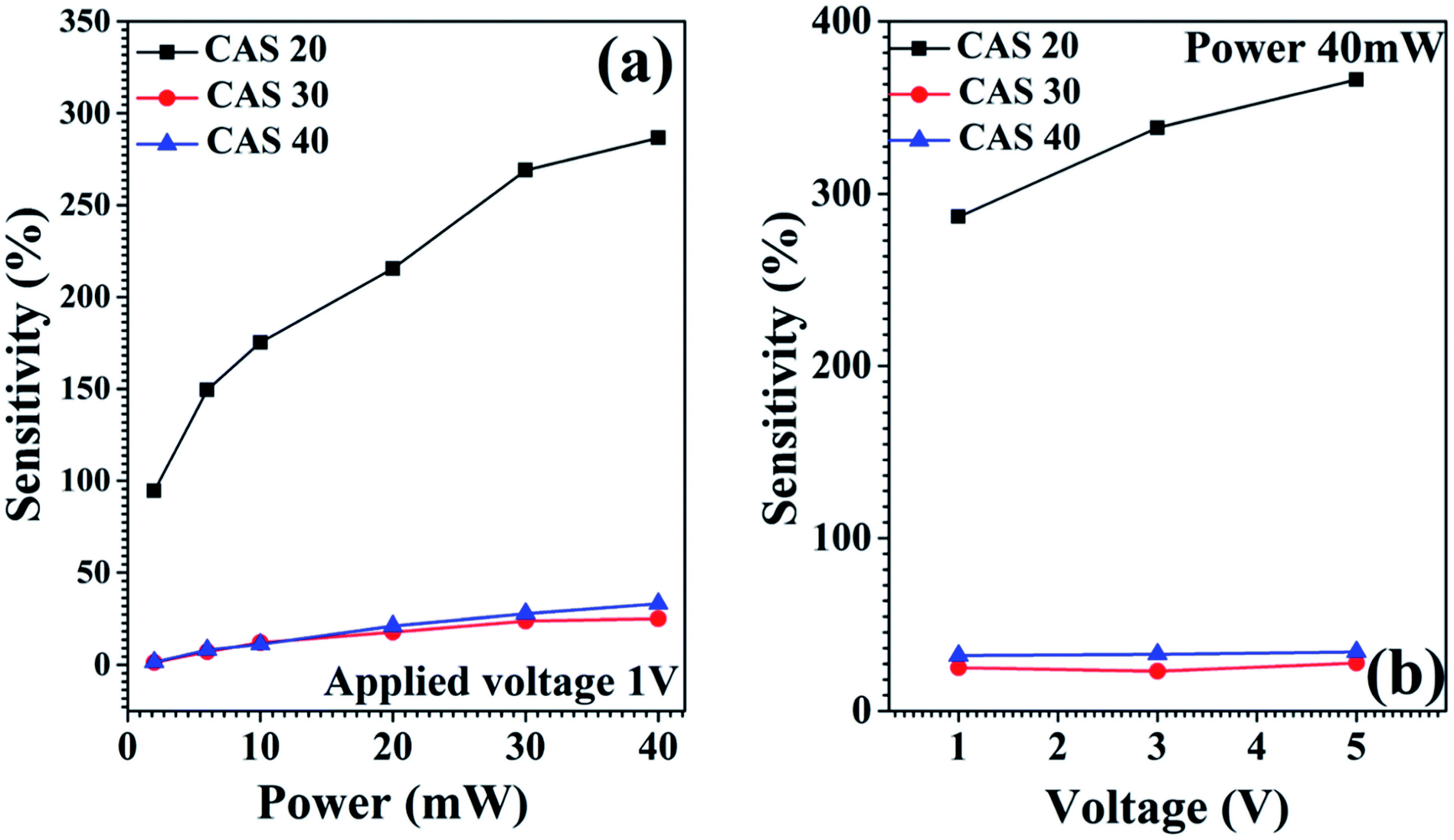
Sensitivity measurements corresponding to the illumination by green laser (532 nm) for different laser power (applied voltage 1 V) as well as for different applied bias voltages (1 V, 3 V and 5 V) are presented in Fig. 9 and the corresponding sensitivity values are shown in Table 2. In accordance with the measurements using LEDs, highest sensitivities are recorded for the CAS 20 sample compared to CAS 30 and CAS 40, while illuminated using the laser. Sensitivity of all the three samples increases gradually with laser intensity. The amount of photocurrent generated per unit area per unit illumination intensity, responsivity (R) is calculated for the structure glass/Sb2S3/Cu/Ag for CAS 20, CAS 30 and CAS 40 from the cyclic photoresponse measurements (Fig. 8) using the following equation,46
| |
 | (5) |
where
Lλ is the power density of the light source. Responsivity of the CAS detectors were calculated using
eqn (5) from the measurements done by laser illumination at applied voltage 1 V and the corresponding values are included in
Table 2. Highest responsivities were recorded for CAS 20 at the laser power of 2 mW, CAS 30 at 10 mW and CAS 40 at 6 mW respectively. Sensitivity measurements of the samples at applied voltages 3 V and 5 V for varying laser power are included in the ESI (Tables ST2 and ST4
†). Our experiments resulted improved photodetection characteristics compared to that of the hybrid photodetector based on CuSbS
2 nanocrystals.
6
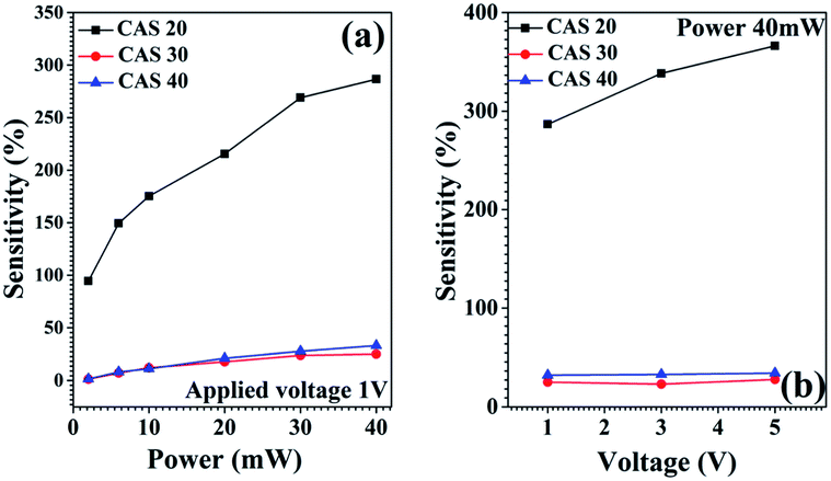 |
| | Fig. 9 (a) Laser power vs. sensitivity graphs of CAS 20, CAS 30 and CAS 40 samples at applied bias voltage 1 V. (b) Sensitivities of CAS 20, CAS 30 and CAS 40 samples for varying bias voltages (1, 3 and 5 V) for the laser power 40 mW. | |
The cyclic stability, linearity and ON/OFF photoresponse of the samples at low applied voltage are the merits of these CAS photodetectors. To check stability, the photoresponsivity of the CAS photodetectors (CAS 20, CAS 30 and CAS 40) were measured under the same illumination conditions and bias voltage, after 5 months of their fabrication. The results are included in ESI (Fig. S10†). The device showed reliable photoconductive properties comparable with the newly fabricated device performance given in Fig. 8.
It is to be noted that in all the samples, the dark current is high due to high electrical conductivity of the samples. The conductivity of a material is an intrinsic property determined by the majority carrier concentration and their mobility. Our previous studies8 showed that CAS films produced by diffusing Cu into Sb2S3 resulted high p-type conductivity due to high hole concentration in the range of 1018 to 1020 cm−3. Also, it is known that p-type conductivity is originated from Cu vacancies in CuSbS2 lattice. Thus, by fine control of Cu/Sb ratio or adding suitable dopants to CuSbS2 without altering the phase purity, the dark conductivity may be modified.
Chalcogenide based binary, ternary and quaternary semiconductors and their composites have already proven to be apt candidates for photodetector applications owing to its unique semiconducting properties. For instance, inorganic thin film visible light photodetector based on graphene on antimony sulfide was reported by Xiao et al.47 and stable photoresponse was obtained even at zero bias voltage for the wavelength range 400–700 nm. In addition, CuInS2 thin film and CuInSe2 nanocrystals were also utilized for light detection applications by various research groups.48,49 Hao et al. reported the synthesis of a high-performance photodetector based on hybrid film of CuSbS2 nanocrystals and poly(3-hexylthiophene).6 Even though the constructed photodetector device had stable photodetection properties, better sensitivity was obtained in the infrared range. In the present work the synthesized CAS thin film photodetectors exhibit photodetection properties for different bias voltages, illumination wavelengths and intensities with excellent stability and reproducibility for the visible as well as NIR regions. The results of this study show that CAS photodetectors are promising optoelectronic devices at large area, low cost, environmentally benign and effective with wavelength-tailorability in visible to NIR backing low applied voltage operation.
4. Conclusions
In summary, we fabricated and characterized CuSbS2 thin films based photodetectors for three different Cu thicknesses (20, 30 and 40 nm). The structure, morphology and opto-electronic properties of the CAS films with special focus on the photodetection application were investigated in detail. Formation of CuSbS2 phase was confirmed by XRD, XPS and Raman analyses and their morphologies by SEM and AFM. Bigger grains were formed in the CAS 40 sample compared to the other two while the optical band gaps of the samples were in the range 1.50–1.63 eV. Photoresponse measurements of all the samples were recorded as a function of incident light wavelength using LEDs as well as function of incident light intensity using a laser. All the samples showed stable, reproducible photoconductive properties with high sensitivity and responsivity for low applied voltage. The present study can help in cost effective production of photodetector devices using environment friendly materials with selective wavelength detection properties at low cost in large area.
Conflicts of interest
There are no conflicts to declare.
Acknowledgements
V. Vinayakumar is thankful to Consejo Nacional de Ciencia y Tecnología (CONACYT-Mexico) for providing a doctoral fellowship. Financial support from CEMIE-Sol Project 35 (SENER-CONACYT, Mexico) is gratefully acknowledged.
References
- D. Aldakov, A. Lefrançois and P. Reiss, J. Mater. Chem. C, 2013, 1, 3756–3776 RSC.
- M. G. Panthani, V. Akhavan, B. Goodfellow, J. P. Schmidtke, L. Dunn, A. Dodabalapur, P. F. Barbara and B. A. Korgel, J. Am. Chem. Soc., 2008, 130, 16770–16777 CrossRef PubMed.
- J.-J. Wang, Y.-Q. Wang, F.-F. Cao, Y.-G. Guo and L.-J. Wan, J. Am. Chem. Soc., 2010, 132, 12218–12221 CrossRef PubMed.
- E. Badradeen, M. Brozak, F. Keles, K. Al-Mayalee and T. Karabacak, J. Vac. Sci. Technol., A, 2017, 35, 03E112 CrossRef.
- A. W. Welch, P. P. Zawadzki, S. Lany, C. A. Wolden and A. Zakutayev, Sol. Energy Mater. Sol. Cells, 2015, 132, 499–506 CrossRef.
- M. Hao, Y. Liu, F. Zhou, L. Jiang, F. Liu and J. Li, ECS Solid State Lett., 2014, 3, Q41–Q43 CrossRef.
- Y. Rodrıguez-Lazcano, M. Nair and P. Nair, J. Cryst. Growth, 2001, 223, 399–406 CrossRef.
- C. Garza, S. Shaji, A. Arato, E. P. Tijerina, G. A. Castillo, T. D. Roy and B. Krishnan, Sol. Energy Mater. Sol. Cells, 2011, 95, 2001–2005 CrossRef.
- B. Yang, L. Wang, J. Han, Y. Zhou, H. Song, S. Chen, J. Zhong, L. Lv, D. Niu and J. Tang, Chem. Mater., 2014, 26, 3135–3143 CrossRef.
- K. Ramasamy, H. Sims, W. H. Butler and A. Gupta, Chem. Mater., 2014, 26, 2891–2899 CrossRef.
- R. Ornelas-Acosta, S. Shaji, D. Avellaneda, G. Castillo, T. D. Roy and B. Krishnan, Mater. Res. Bull., 2015, 61, 215–225 CrossRef.
- W. Septina, S. Ikeda, Y. Iga, T. Harada and M. Matsumura, Thin Solid Films, 2014, 550, 700–704 CrossRef.
- L. Yu, R. S. Kokenyesi, D. A. Keszler and A. Zunger, Adv. Energy Mater., 2013, 3, 43–48 CrossRef.
- E. Peccerillo, J. Major, L. Phillips, R. Treharne, T. J. Whittles, V. Dhanak, D. Halliday and K. Durose, IEEE 40th Photovoltaic Specialist Conference (PVSC), 2014, pp. 0266–0269 Search PubMed.
- S. C. Riha, A. A. Koegel, J. D. Emery, M. J. Pellin and A. B. Martinson, ACS Appl. Mater. Interfaces, 2017, 9, 4667–4673 CrossRef PubMed.
- S. Banu, S. J. Ahn, S. K. Ahn, K. Yoon and A. Cho, Sol. Energy Mater. Sol. Cells, 2016, 151, 14–23 CrossRef.
- A. W. Welch, L. L. Baranowski, P. Zawadzki, C. DeHart, S. Johnston, S. Lany, C. A. Wolden and A. Zakutayev, Prog. Photovoltaics, 2016, 24, 929–939 Search PubMed.
- F. W. de Souza Lucas, A. W. Welch, L. L. Baranowski, P. C. Dippo, H. Hempel, T. Unold, R. Eichberger, B. Blank, U. Rau and L. H. Mascaro, J. Phys. Chem. C, 2016, 120, 18377–18385 CrossRef.
- W. Wubet and D.-H. Kuo, Mater. Res. Bull., 2014, 53, 290–294 CrossRef.
- C. Marino, T. Block, R. Pöttgen and C. Villevieille, J. Power Sources, 2017, 342, 616–622 CrossRef.
- Z. Zhang, C. Zhou, Y. Liu, J. Li, Y. Lai and M. Jia, Int. J. Electrochem. Sci., 2013, 8, e10067 Search PubMed.
- Z. Zhang, Y. Fu, C. Zhou and Y. Lai, J. Electron. Mater., 2015, 44, 252–257 CrossRef.
- M. Nair, Y. Pena, J. Campos, V. Garcia and P. Nair, J. Electrochem. Soc., 1998, 145, 2113–2120 CrossRef.
- I. Popovici and A. Duta, Int. J. Photoenergy, 2012, 2012, 962649 CrossRef.
- A. Rastogi and N. Janardhana, Thin Solid Films, 2014, 565, 285–292 CrossRef.
- A. Rabhi, M. Kanzari and B. Rezig, Thin Solid Films, 2009, 517, 2477–2480 CrossRef.
- R. Mane and C. Lokhande, Mater. Chem. Phys., 2000, 65, 1–31 CrossRef.
- P. Nair, M. Nair, V. Garcıa, O. Arenas, Y. Pena, A. Castillo, I. Ayala, O. Gomezdaza, A. Sanchez and J. Campos, Sol. Energy Mater. Sol. Cells, 1998, 52, 313–344 CrossRef.
- V. Vinayakumar, S. Shaji, D. Avellaneda, T. D. Roy, G. Castillo, J. Martinez and B. Krishnan, Sol. Energy Mater. Sol. Cells, 2017, 164, 19–27 CrossRef.
- B. Krishnan, A. Arato, E. Cardenas, T. D. Roy and G. Castillo, Appl. Surf. Sci., 2008, 254, 3200–3206 CrossRef.
- Y. Rodríguez Lazcano, L. Guerrero, O. Gomez Daza, M. Nair and P. Nair, Superficies y vacio, 1999 Search PubMed.
- C. Macías, S. Lugo, Á. Benítez, I. López, B. Kharissov, A. Vázquez and Y. Peña, Mater. Res. Bull., 2017, 87, 161–166 CrossRef.
- J. A. Ramos Aquino, D. L. Rodriguez Vela, S. Shaji, D. A. Avellaneda and B. Krishnan, Phys. Status Solidi C, 2016, 13, 24–29 CrossRef.
- D. Colombara, L. M. Peter, K. D. Rogers, J. D. Painter and S. Roncallo, Thin Solid Films, 2011, 519, 7438–7443 CrossRef.
- A. Bushroa, R. Rahbari, H. Masjuki and M. Muhamad, Vacuum, 2012, 86, 1107–1112 CrossRef.
- J. Baker, R. S. Kumar, D. Sneed, A. Connolly, Y. Zhang, N. Velisavljevic, J. Paladugu, M. Pravica, C. Chen and A. Cornelius, J. Alloys Compd., 2015, 643, 186–194 CrossRef.
- C. L. McCarthy, P. Cottingham, K. Abuyen, E. C. Schueller, S. P. Culver and R. L. Brutchey, J. Mater. Chem. C, 2016, 4, 6230–6233 RSC.
- S. Thiruvenkadam and A. L. Rajesh, International Journal of Scientific & Technology Research, 2014, 3, 38–41 Search PubMed.
- H. Guo, Y. Cui, Q. Tian, S. Gao, G. Wang and D. Pan, Cryst. Growth Des., 2015, 15, 771–777 CrossRef.
- I. Efthimiopoulos, C. Buchan and Y. Wang, Sci. Rep., 2016, 6, 24246 CrossRef PubMed.
- B. Minceva-Sukarova, M. Najdoski, I. Grozdanov and C. Chunnilall, J. Mol. Struct., 1997, 410, 267–270 Search PubMed.
- (http://rruff.info).
- T. J. Whittles, T. D. Veal, C. N. Savory, A. W. Welch, F. W. de Souza Lucas, J. T. Gibbon, M. Birkett, R. J. Potter, D. O. Scanlon and A. Zakutayev, ACS Appl. Mater. Interfaces, 2017, 9, 41916–41926 CrossRef PubMed.
- O. Lopez-Sanchez, D. Lembke, M. Kayci, A. Radenovic and A. Kis, Nat. Nanotechnol., 2013, 8, 497 CrossRef PubMed.
- M. S. Mahdi, K. Ibrahim, A. Hmood, N. M. Ahmed, S. A. Azzez and F. I. Mustafa, RSC Adv., 2016, 6, 114980–114988 RSC.
- T. S. Reddy and M. S. Kumar, RSC Adv., 2016, 6, 95680–95692 RSC.
- Y. Xiao, C. Li, X. Tan, L. Zhang, Y. Zhong and H. Zhu, Sol. RRL, 2017, 1, 1770146 CrossRef.
- S. Bulyarsky, L. Vostretsova and S. Gavrilov, Semiconductors, 2016, 50, 106–111 CrossRef.
- R. Guo, T. Shen and J. Tian, J. Mater. Chem. C, 2018, 6, 2573–2579 RSC.
Footnote |
| † Electronic supplementary information (ESI) available. See DOI: 10.1039/c8ra05662e |
|
| This journal is © The Royal Society of Chemistry 2018 |
Click here to see how this site uses Cookies. View our privacy policy here. 
 Open Access Article
 This Open Access Article is licensed under a Creative Commons Attribution-Non Commercial 3.0 Unported Licence
 a,
S. Shaji
a,
S. Shaji