
 Open Access Article
 This Open Access Article is licensed under a Creative Commons Attribution-Non Commercial 3.0 Unported Licence
Triangular radial Nb2O5 nanorod growth on c-plane sapphire for ultraviolet-radiation detection†
Kwan-Woo Kim‡
a,
Bum Jun Kim‡b,
Sang Hoon Leea,
Tuqeer Nasirb,
Hyung-Kyu Lima,
Ik Jun Choia,
Byung Joo Jeonga,
Jaeyeong Leec,
Hak Ki Yu c and
Jae-Young Choi*ab
c and
Jae-Young Choi*ab
aSchool of Advanced Materials Science and Engineering, Sungkyunkwan University, Suwon, 16419, Korea. E-mail: jy.choi@skku.edu
bSKKU Advanced Institute of Nanotechnology (SAINT), Sungkyunkwan University, Suwon, 16419, Korea
cDepartment of Materials Science and Engineering, Department of Energy Systems Research, Ajou University, Suwon, 16499, Korea
First published on 4th September 2018
Abstract
Nb2O5 nanostructures with excellent crystallinities were grown on c-plane sapphire and employed for ultraviolet-(UV)-radiation detection. The triangular radial Nb2O5 grown on the c-sapphire substrate had a 6-fold symmetry with domain matching epitaxy on the substrate. Owing to the radial growth, the nanorods naturally connected when the deposition time increased. This structure can be used as a UV-detector directly by depositing macroscale electrodes without separation of a single nanorod and e-beam lithography process. It was confirmed that electric reactions occur at different UV irradiation wavelengths (254 nm and 365 nm).
Introduction
Ultraviolet rays (UV) are electromagnetic waves with shorter wavelengths than those of visible light, mainly in the range of 200 nm to 400 nm.1 UV irradiation affecting our lives can be divided into two types: (i) generated from the sun, reaching the earth through cosmic radiation, and (ii) those emerging from various chemical reactions on the earth. UV irradiation generated from the sun is mostly absorbed by various molecules in the atmosphere (CO2, H2O, etc.); radiation reaching the surface is in the region of UV-A (320–400 nm).1 UV-A can have positive effects, such as sterilisation, or side effects such as occurrence of skin cancer. On the other hand, UV radiation generated by various chemical reactions produced by humans varies from UV-A to UV-C (UV-B: 290–320 nm and UV-C: 200–290 nm). Both efficient use of the generated UV radiation and its blockage for safety purposes are important.In this regard, one of the most important factors is the efficient UV detection. Theoretically, one of the best approaches to detect UV irradiation is to measure changes in electrical conductivity of an UV-irradiated material with band gap.1–5 It is important to select a material with an appropriate band gap (Eg > 3.1 eV) in order to detect UV radiation in the range of 200 nm to 400 nm (UV-A to UV-C regions). However, if the band gap is too large, the material is close to insulator and the electron excitation effect due to UV absorption is not sufficient to detect.
In this study, we aimed to implement a UV-radiation detector using Nb2O5 with an ideal band-gap energy in the range of 3.5 eV to 4.8 eV (photon energy of 354 nm to 258 nm)6–8 and chemical stability9–11 for UV detection. It has already been shown by Fang et al.12 and Liu et al.13 that Nb2O5 can be used as a UV detector and has high responsivity. In addition, the Nb2O5 UV detector was recently synthesized using a simple and low cost hydrothermal method.14 In order to develop the UV-detector using Nb2O5, materials with good crystallinities should be synthesised, as when a defect is present in Nb2O5, light absorption occurs due to the defect levels (532 nm: 2.3 eV and 808 nm: 1.5 eV). In the case of thin-film or bulk syntheses, the possibility of occurrence of defects such as grain boundaries in the synthesised material increases. We aimed to synthesise nanoscale single-crystal Nb2O5 (various structures of Nb2O5 nanomaterials were used for applications to gas sensors,15,16 photo-catalysts,17,18 photo-detectors,12,19 batteries,20,21 solar cells,22,23 etc.). In addition, if the detector device is fabricated using a single nanorod,11,24–28 the fabrication is complex (such as e-beam lithography), leading to a lower productivity and higher process costs. Therefore, in this study, synthesis conditions (substrate type and orientation, precursor of Nb, growth temperature, and reaction/carrier gas) were investigated so that synthesised Nb2O5 nanostructures could be naturally connected to each other to enable to immediately use the device when only macroscale electrodes are deposited.
Experimental
Growth of Nb2O5 nanostructures
The growth of Nb2O5 was performed on a single-crystal c-plane sapphire substrate (Namkang Hi-tech Co., Ltd., SaR 100-500) using a quartz tube furnace. NbCl5 (Alfa Aesar, #11548), used as a Nb precursor, was placed in a stainless-steel canister, which was heated by a heating mantle. The sublimed NbCl5 and Ar carrier gas were introduced into the tube through a 1/4 inch stainless-steel gas line, which was wrapped and heated by a commercial heating tape. The temperatures of the canister and line were maintained at 140 °C and 160 °C, respectively.For cleaning, the sapphire substrates were sonicated in acetone, alcohol, and deionised (DI) water for 15 min in each solvent. The sapphire substrates were then loaded into the tube furnace and the system was pumped down to vacuum and refilled with Ar gas to obtain atmospheric pressure. The furnace temperature was increased to 900 °C within 40 min in Ar environment with an Ar gas flow of 200 sccm. After the temperature reached 900 °C, the growth of Nb2O5 was initiated by introducing another flow (200 sccm) of Ar carrier gas through the canister to the furnace. After the growth, the Nb-precursor supply line was closed, and the samples were rapidly cooled down under the Ar environment.
Analysis and measurement
An X-ray diffractometer (Bruker D8-Advance with monochromated Cu-Kα1 radiation; scan rate of 0.05° s−1) was used for identification of the sample. A pole figure analysis was performed to study the symmetry of the sample using an X-ray diffractometer (PANalytical, X'pert PRO using Cu-Kα radiation, χ: 0–75° and φ: 0–360° at 2θ of 25°). The surface morphology and cross-section structure of the sample were investigated by SEM (Hitachi, S-4800). Transmission electron microscopy (TEM) (JEOL, JEM-2100F, at 200 kV) was employed to analyse the structures and growth directions of the rods. A UV/visible spectrometer (Shimadzu, UV-3600) was used to measure the optical transmittance of the material. A current–voltage (I–V) curve and time-dependent response of the UV detector were obtained using a probe station (MSTECH, MST5000). A single-wavelength (254 nm/365 nm) UV lamp (VILBER, VL-215 LC) was used as the UV source.Results and discussion
To understand the effect of the substrate on the growth of the Nb2O5 nanorods, we performed SEM on Nb2O5 synthesised on three types of substrates (SiO2/Si, graphene-coated Ni foil, and c-plane (0006) sapphire substrate; see Fig. 1a). On the graphene/Ni surface, irregularly sized structures are observed, while on the other two substrates (SiO2/Si and c-plane sapphire), nanorods with uniform sizes were synthesised. The irregularities observed on the graphene surface can be interpreted as a phenomenon in which niobium oxide nuclei cannot be easily generated owing to the low surface energy of the graphene surface (40–50 mJ m−2) compared to those of SiO2/Si (∼800 mJ m−2) and c-plane sapphire (∼1900 mJ m−2).29–31 X-ray diffraction (XRD) was performed to characterise the nanorod alignments on SiO2/Si and c-plane sapphire (Fib. 1b). The Nb2O5 nanorods deposited on the c-plane sapphire substrate have a preferential orientation of the monoclinic (−713) plane (Joint Committee on Powder Diffraction Standards (JCPDS) no. 37-1468),32 whereas those on the SiO2/Si substrate are relatively randomly oriented and have low crystallinities.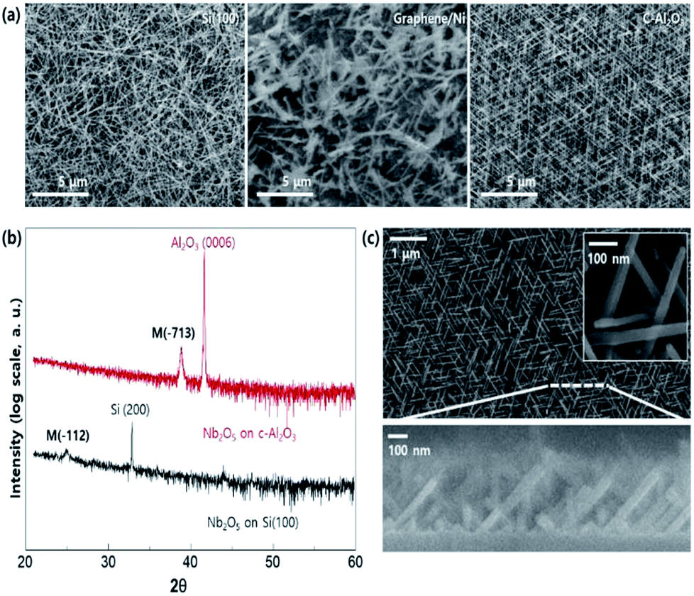 | ||
| Fig. 1 (a) Scanning electron microscopy (SEM) images of Nb2O5 nanorods grown for 90 min on different substrates. (b) X-ray diffraction (XRD) patterns of Nb2O5 on c-plane sapphire (top) and Si (100) (bottom). (c) SEM images of Nb2O5 nanorods grown on c-plane sapphire for 30 min. | ||
SEM images (Fig. 1c) of the sample obtained with a reduced deposition time (Fig. 1a and c show the samples deposited for 90 min and 30 min, respectively) confirm the preferential orientation of Nb2O5 deposited on the c-plane sapphire and reveal that equilateral triangular nanostructures were uniformly distributed with a tilting angle of approximately 45° with respect to the substrate.
TEM was performed to understand the regularity of the Nb2O5 nanorods grown on the c-plane sapphire crystal. As shown in Fig. 2a and b, the Nb2O5 nanorod with a (−112) growth direction has a tilting angle of 45.01° with respect to the (−713) plane, which is the preferred orientation, as shown in the XRD measurement (Fig. 2c and 1b). In addition, the result that no metallic component was detected in the head of the Nb2O5 nanorod reveals that Nb, decomposed from the NbCl5 precursor, combines with remaining oxygen in the furnace to form Nb2O5 directly, referred to as vapour–solid growth mechanism.33–35
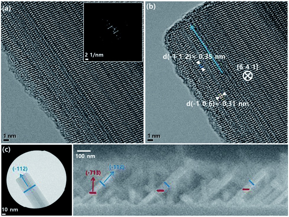 | ||
| Fig. 2 (a and b) High-resolution TEM images and selected-area electron diffraction (SAED) pattern of a single Nb2O5 nanorod. The SAED pattern was recorded from the Nb2O5 nanorod shown in (c). (c) Low-magnification TEM image (left) and cross-section SEM image (right) of a single Nb2O5 nanorod. | ||
The X-ray pole figure of the Nb2O5/c-sapphire system was measured to understand the triangular arrangement of the nanorods. When the pole figure is measured at a tilting angle (χ) of 55°, the part with a 6-fold symmetry and that with a 3-fold symmetry are mixed, as shown in Fig. 3a and b. The sapphire (102) plane is tilted at 57.6° with respect to the (006) plane (referred to as c-plane) and has a 3-fold symmetry; therefore, the 3-fold symmetry (green circles in Fig. 3a) corresponds to the sapphire substrate. The remaining structures with the 6-fold symmetry can be attributed to the synthesised Nb2O5. Nb2O5, which has a monoclinic structure, usually has a 2-fold symmetry; however, it can have a 6-fold symmetry if intervals of 120° are observed. Fig. 3c shows the cell shape of the monoclinic (−713) plane of Nb2O5 (a = 12.483 nm, b = 7.244 nm, α = 90°, and γ = 61.166°; the black circles represent O atoms). The epitaxial growth along the Nb2O5 (−713) plane on the c-plane sapphire substrate with an interatomic distance of 0.275 nm can be explained by domain matching epitaxy (DME).36–38 The length of 45 atomic spacings of Al2O3 is 12.375 nm (0.275 nm × 45 = 12.375 nm), which implies a domain mismatch with the Nb2O5 a-axis of approximately 0.108 nm, while that of 3 atomic spacings of Al2O3 is 0.825 nm (0.275 nm × 3 = 0.825 nm), corresponding to a domain mismatch with the Nb2O5 b-axis of approximately 0.101 nm, leading to the hexagonal arrangement shown in Fig. 3d.
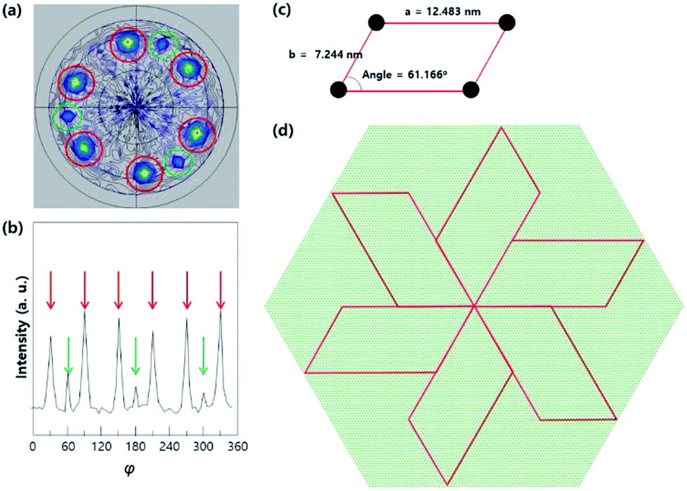 | ||
| Fig. 3 (a) X-ray pole figure of the Nb2O5/c-sapphire system measured at a 2θ angle of 25.05° for the monoclinic Nb2O5 (−112) peak. Red and green circles represent the peaks of Nb2O5 nanorods and sapphire substrate, respectively. (b) Azimuthal (φ) scan data measured at a χ angle of 55°. (c) Cell shape of the monoclinic Nb2O5 (−713) plane. (d) Schematic of the hexagonal arrangement of the monoclinic Nb2O5 (−713) plane on the c-sapphire substrate. | ||
The synthesised triangular radial Nb2O5 nanorods have excellent crystal qualities, which suggests that they have excellent properties in terms of UV absorption. Fig. 4a shows the UV-visible transmittance of the Nb2O5/c-sapphire sample. At approximately 400 nm, the light absorption is approximately 20%; with the decrease in the wavelength, the absorption increases (95% at 280 nm). As shown in the first-order differential form of the transmission spectrum (Fig. 4b), this absorption tendency is most prominent at approximately 300 nm, which implies that the synthesised Nb2O5 on c-sapphire can be effectively employed in a wide UV-detection range (from A to C). In addition, we could see the changes in the UV absorption behaviour through the comparison with the UV-visible transmittance spectrum of the sample grown for a longer time (Fig. S1†). As the synthesis time increased, the density of the nanorods increased and the nanorods were more cross-linked as shown in Fig. 1a and b, resulting in the change in the UV transmittance behaviour. Not only did the absolute amount of absorbed light increase, but also the absorption range was up-shifted by approximately 30 nm (see the change of the wavelength at which the slope of the graph changes from positive to negative). Furthermore, the relation of the UV-absorption to the synthesis temperature could also be deduced. As the synthesis temperature was lower, the density of nanorods decreased, and the nanorods were less cross-linked (see Fig. S2†). Based on the relationship between nanorods density and UV-absorption that we have seen above, it can be inferred that the higher the temperature, the greater the amount of UV absorbed.
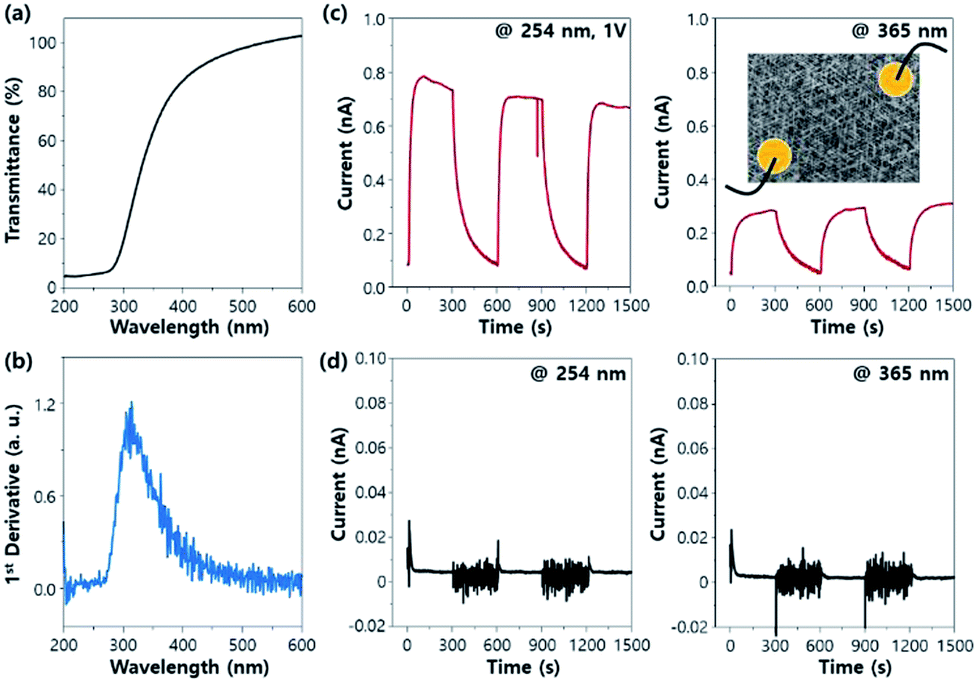 | ||
| Fig. 4 (a) UV-visible transmittance spectrum of the Nb2O5/c-sapphire system and (b) its 1st derivative. Photo-conductivity of Nb2O5 grown on (c) c-sapphire and (d) Si (100) illuminated with lights with wavelengths of (left) 254 nm and (right) 365 nm at an applied voltage of 1 V. | ||
The triangular radial Nb2O5 nanorods deposited on the c-sapphire substrate are connected to each other using a longer deposition time. Therefore, the system can be directly used as a UV-radiation detector without separation of nanorods and e-beam lithography process; i.e., the device can be fabricated by directly depositing macroscale electrodes (shown in the inset schematics of Fig. 4c at a UV wavelength of 365 nm). In the Nb2O5/c-sapphire structure, distinct photoreactions are observed at UV wavelengths of 254 nm and 365 nm at an applied constant voltage of 1 V. The shorter UV wavelength provides a larger current (Fig. 4c). The current value increases as the applied voltage increases and has a linear relationship with the applied voltage. Fig. S3† shows the I–V curve of Nb2O5 grown on c-sapphire while illuminating UV light. The Nb2O5/Si structure exhibits photo-reactivity; however, the signal is very small, hindering its application as an actual device (Fig. 4d). Through this process, Nb2O5 nanorods with excellent crystallinities and self-connection can be easily employed for UV-radiation detection devices. The spectra responsivity (Rλ) and external quantum efficiency (EQE) are two critical parameters to show the performance of the UV detector.12 They are expressed as Rλ = ΔI/PS and EQE = Rλhc/eλ, respectively, where ΔI is the difference between the photo-excited current and dark current, P is the light power density, S is the irradiated area, h is Planck's constant, c is the velocity of light, e is the electronic charge, and λ is the exciting wavelength. The calculated Rλ and EQE of the Nb2O5 on c-plane sapphire at 1 V are 1.87 × 10⁻³ A W−1 and 0.913% when irradiated with 254 nm UV and 1.76 × 10⁻⁴ A W−1 and 0.060% when irradiated by 365 nm UV. These values are difficult to compare with those of the other materials with nanowire (rod) network or mat structure as with ours reported in the literature because they were hardly evaluated by Rλ and EQE values, and even if evaluated, they were evaluated in microscale. These values are usually measured for a single nanowire,39 nanobelt,12 and nanoplate13 between microscale electrodes in the literature. There was one paper that measured Rλ value of Nb2O5 nanomoss structure in macroscale, where the Rλ at 10 V is 2.43 × 10⁻³ A W−1 when irradiated with 365 nm UV.14 Considering that a voltage 10 times higher than the voltage we applied was used, it can be inferred that the increased ΔI value due to the higher V led to the larger Rλ value than ours. The ΔI–V relationship for our sample is shown in Fig. S3.† However, the Rλ and EQE values of our sample are significantly smaller than those of single Nb2O5 nanobelt (15.2 A W−1 with 320 nm at 1 V)12 and nanoplate (24.7 A W−1 with 320 nm at 1 V)13 reported in other articles. Unlike them, our measurements are not on a single nanorod but on inter-connected rods between the macroscale electrodes. Therefore, carrier transport must occur not only within nanorods but also between nanorods. In the case of transport between nanorods, carriers must overcome the junction barrier at the interface between the nanorods to move from one nanorod to another.12,39,40 The low measured values can be attributed to the numerous transport processes that carriers experience when moving through the macroscale channel.
Conclusions
Nb2O5 nanostructures with excellent crystallinities were grown on c-plane sapphire and their UV-detection performance was measured. The grown Nb2O5 on the c-sapphire substrate had a 6-fold symmetry with DME on the substrate; the results confirmed the radial growth. Owing to the radial growth, the nanorods naturally connected when the deposition time increased. This structure can be used as a UV-radiation detector directly by depositing macroscale electrodes without separation of a single nanorod and e-beam lithography process. It was confirmed that electric reactions occur at different UV irradiation wavelengths (254 nm and 365 nm). Therefore, it is expected that the structure can be easily employed in the development of a large-area UV sensor.Conflicts of interest
There are no conflicts to declare.Acknowledgements
This research was supported by Basic Science Research Program through the National Research Foundation of Korea (NRF) funded by the Ministry of Education, Science and Technology (NRF-2018R1D1A1B07050253). We gratefully thank Tae-Woo Lee of RIAM (Research Institute of Advanced Materials) for XRD and Pole figure measurement.Notes and references
- X. Fang, Y. Bando, U. K. Gautam, T. Zhai, H. Zeng, X. Xu, M. Liao and D. Golberg, Crit. Rev. Solid State Mater. Sci., 2009, 34, 190–223 CrossRef.
- K.-J. Chen, F.-Y. Hung, S.-J. Chang and S.-J. Young, J. Alloys Compd., 2009, 479, 674–677 CrossRef.
- H. Wu, Y. Sun, D. Lin, R. Zhang, C. Zhang and W. Pan, Adv. Mater., 2009, 21, 227–231 CrossRef.
- N. Gogurla, A. K. Sinha, S. Santra, S. Manna and S. K. Ray, Sci. Rep., 2014, 4, 6483 CrossRef PubMed.
- Y. Xie, L. Wei, G. Wei, Q. Li, D. Wang, Y. Chen, S. Yan, G. Liu, L. Mei and J. Jiao, Nanoscale Res. Lett., 2013, 8, 188 CrossRef PubMed.
- J. W. Schultze and M. Lohrengel, Electrochim. Acta, 2000, 45, 2499–2513 CrossRef.
- T. Proslier, J. Zasadzinski, L. Cooley, M. Pellin, J. Norem, J. Elam, C. Z. Antoine, R. A. Rimmer and P. Kneisel, IEEE Trans. Appl. Supercond., 2009, 19, 1404–1408 Search PubMed.
- S. Zhuiykov and E. Kats, World Academy of Science, Engineering and Technology, 2013, vol. 78, p. 484 Search PubMed.
- R. Jose, V. Thavasi and S. Ramakrishna, J. Am. Ceram. Soc., 2009, 92, 289–301 CrossRef.
- H. Luo, W. Song, P. G. Hoertz, K. Hanson, R. Ghosh, S. Rangan, M. K. Brennaman, J. J. Concepcion, R. A. Binstead and R. A. Bartynski, Chem. Mater., 2012, 25, 122–131 CrossRef.
- L. Alibabaei, H. Luo, R. L. House, P. G. Hoertz, R. Lopez and T. J. Meyer, J. Mater. Chem. A, 2013, 1, 4133–4145 RSC.
- X. Fang, L. Hu, K. Huo, B. Gao, L. Zhao, M. Liao, P. K. Chu, Y. Bando and D. Golberg, Adv. Funct. Mater., 2011, 21, 3907–3915 CrossRef.
- H. Liu, N. Gao, M. Liao and X. Fang, Sci. Rep., 2015, 5, 7716 CrossRef PubMed.
- R. Abdul Rani, A. S. Zoolfakar, N. S. Khairir, M. H. Mamat, S. Alrokayan, H. A. Khan and M. R. Mahmood, J. Mater. Sci.: Mater. Electron., 2018, 29, 1–10 CrossRef.
- Z. Wang, Y. Hu, W. Wang, X. Zhang, B. Wang, H. Tian, Y. Wang, J. Guan and H. Gu, Int. J. Hydrogen Energy, 2012, 37, 4526–4532 CrossRef.
- R. A. Rani, A. S. Zoolfakar, J. Z. Ou, M. R. Field, M. Austin and K. Kalantar-Zadeh, Sens. Actuators, B, 2013, 176, 149–156 CrossRef.
- K. Sayama, H. Sugihara and H. Arakawa, Chem. Mater., 1998, 10, 3825–3832 CrossRef.
- H. Kominami, K. Oki, M. Kohno, S.-i. Onoue, Y. Kera and B. Ohtani, J. Mater. Chem., 2001, 11, 604–609 RSC.
- L. Sang, M. Liao and M. Sumiya, Sensors, 2013, 13, 10482–10518 CrossRef PubMed.
- H. Nakazawa, K. Sano, T. Abe, M. Baba and N. Kumagai, J. Power Sources, 2007, 174, 838–842 CrossRef.
- B. Reichman and A. J. Bard, J. Electrochem. Soc., 1981, 128, 344–346 CrossRef.
- M. K. Siddiki, S. Venkatesan and Q. Qiao, Phys. Chem. Chem. Phys., 2012, 14, 4682–4686 RSC.
- O. Wiranwetchayan, Z. Liang, Q. Zhang, G. Cao and P. Singjai, Mater. Sci. Appl., 2011, 2, 1697 Search PubMed.
- C. Soci, A. Zhang, B. Xiang, S. A. Dayeh, D. Aplin, J. Park, X. Bao, Y.-H. Lo and D. Wang, Nano Lett., 2007, 7, 1003–1009 CrossRef PubMed.
- Y. Jiang, W. J. Zhang, J. S. Jie, X. M. Meng, X. Fan and S. T. Lee, Adv. Funct. Mater., 2007, 17, 1795–1800 CrossRef.
- J.-J. Wang, F.-F. Cao, L. Jiang, Y.-G. Guo, W.-P. Hu and L.-J. Wan, J. Am. Chem. Soc., 2009, 131, 15602–15603 CrossRef PubMed.
- L. Li, X. Fang, T. Zhai, M. Liao, U. K. Gautam, X. Wu, Y. Koide, Y. Bando and D. Golberg, Adv. Mater., 2010, 22, 4151–4156 CrossRef PubMed.
- Y. Zhang, J. Wang, H. Zhu, H. Li, L. Jiang, C. Shu, W. Hu and C. Wang, J. Mater. Chem., 2010, 20, 9858–9860 RSC.
- H. K. Yu and J.-L. Lee, Sci. Rep., 2014, 4, 6589 CrossRef PubMed.
- D. T. Danielson, D. K. Sparacin, J. Michel and L. C. Kimerling, J. Appl. Phys., 2006, 100, 083507 CrossRef.
- J. Guo, D. Ellis and D. Lam, Phys. Rev. B, 1992, 45, 3204 CrossRef.
- S. Heusing, D.-L. Sun, J. Otero-Anaya and M. A. Aegerter, Thin Solid Films, 2006, 502, 240–245 CrossRef.
- Y. Zhang, N. Wang, S. Gao, R. He, S. Miao, J. Liu, J. Zhu and X. Zhang, Chem. Mater., 2002, 14, 3564–3568 CrossRef.
- A. Umar, S. Kim, Y.-S. Lee, K. Nahm and Y. Hahn, J. Cryst. Growth, 2005, 282, 131–136 CrossRef.
- Y. L. Chueh, M. W. Lai, J. Q. Liang, L. J. Chou and Z. L. Wang, Adv. Funct. Mater., 2006, 16, 2243–2251 CrossRef.
- H. K. Yu and J.-L. Lee, Cryst. Growth Des., 2010, 10, 5200–5204 CrossRef.
- F. Sánchez, R. Bachelet, P. de Coux, B. Warot-Fonrose, V. Skumryev, L. Tarnawska, P. Zaumseil, T. Schroeder and J. Fontcuberta, Appl. Phys. Lett., 2011, 99, 211910 CrossRef.
- W.-R. Liu, Y.-H. Li, W. Hsieh, C.-H. Hsu, W. Lee, Y. Lee, M. Hong and J. Kwo, Cryst. Growth Des., 2008, 9, 239–242 CrossRef.
- M. Chen, L. Hu, J. Xu, M. Liao, L. Wu and X. Fang, Small, 2011, 7, 2449–2453 Search PubMed.
- S. Jeong, M. W. Kim, Y.-R. Jo, Y.-C. Leem, W.-K. Hong, B.-J. Kim and S.-J. Park, Nano Energy, 2016, 30, 208–216 CrossRef.
Footnotes |
| † Electronic supplementary information (ESI) available. See DOI: 10.1039/c8ra06139d |
| ‡ These authors contributed equally to this study. |
| This journal is © The Royal Society of Chemistry 2018 |