
 Open Access Article
 This Open Access Article is licensed under a
 Creative Commons Attribution 3.0 Unported Licence
Ab initio quantum transport in AB-stacked bilayer penta-silicene using atomic orbitals†
Eleni Chatzikyriakou *a,
Padeleimon Karafilogloub and
Joseph Kioseogloua
*a,
Padeleimon Karafilogloub and
Joseph Kioseogloua
aDepartment of Physics, Aristotle University of Thessaloniki, 54124 Thessaloniki, Greece. E-mail: elchatz@auth.gr; Tel: +30 2310 998109
bLaboratory of Applied Quantum Chemistry, Department of Chemistry, Aristotle University of Thessaloniki, POB 135, 54124 Thessaloniki, Greece
First published on 3rd October 2018
Abstract
The current carried by a material subject to an electric field is microscopically inhomogeneous and can be modelled using scattering theory, in which electrons undergo collisions with the microscopic objects they encounter. We herein present a methodology for parameter-free calculations of the current density from first-principles using density functional theory, Wannier functions and scattering matrices. The methodology is used on free-standing AB-stacked bilayer penta-silicene. This new Si allotrope has been proposed to have a higher stability than any of its hexagonal bilayer counterparts. Furthermore, its semiconducting properties make it ideal for use in electronic components. We unveil the role of the pz orbitals in the transport through a three-dimensional quantum wire and present current density streamlines that reveal the locations of the highest charge flow. The present methodology can be expanded to accommodate many electron degrees of freedom, the application of electromagnetic fields and many other physical phenomena involved in device operation.
1 Introduction
Recent advances in fabrication techniques1 and inkjet printing of 2D materials2 have brought the principles of mesoscopic physics into the foreground in order to explain and predict electron device behaviour in a wide range of occasions. In resistive switching memory devices (RRAM), where a conductive filament is formed under the application of a voltage at the electrodes,3,4 conductance quantization has been observed5 and the SET operation has been modelled using the Landauer formula for electron tunnelling.6 ’Filaments' have also been studied in relation to the atomic structure of graphene sheets theoretically7 while the transition from quantum to classical regime with the use of weighted phonon self-energies has been modelled using networks of sites and the Keldysh Green function formalism.8 These methods can serve as a valuable tool for explaining experimental topography9 and scanning tunnelling potentiometry.10Silicon has historically been the most widely used semiconducting material in the electronics industry both due to its abundance in nature and due to the low-defect interface that it forms with the insulating SiO2 used in transistors and other electronic components. Hexagonal silicene11,12 was one of the first two-dimensional sensations with a plenitude of novel properties, however, when compared to its Dirac cone counterpart, graphene, silicene has a much smaller elastic constant13 and this poses difficulties in its manipulation in the lab.
Other forms of silicon derivatives have been the focus of studies using systematic materials search, revealing novel allotropes with direct band-gaps14 and even high mobility values.15 Penta-silicene is a new form of monolayer silicon that has been observed recently.16,17 Pentagons are rare atomic configurations that are less frequently studied than hexagonal structures mainly due to their difficulties imposed in their fabrication. Using first principles calculations, bilayer penta-silicene, whose layers are stacked in 90° angle between them has been found to be more stable than the most stable form of bilayer hexagonal silicene.18 It is made up of pentagonal rings of Si atoms, similar to penta-graphene19 and other two-dimensional penta-structures.20 Twisting angles between the layers of few-layer materials has been proved to be an efficient method for tuning their properties.21,22 Contrary to the bilayer form with no twisting angle, the AB stacking configuration of penta-silicene has semiconducting properties. This makes it ideal for many different configurations of electronic devices, stemming from the recent surge in heterostructure fabrication.23
In the structures that we examine herein, parts of the system lose their symmetry in favour of stability. Situations such as this, call for the more intuitive chemical description of the system in terms of its valence bonding configuration and this can be very well described with the use of maximally localized Wannier functions (WFs). The latter, acting as alternative representations of Bloch orbitals, have recently gained popularity for examining a plethora of mesoscopic phenomena due to advancements in localization techniques24,25 but also when used as tools for high-throughput screening of topological materials.26 Even more interesting for this study, is the possibility to derive model Tight Binding (TB) Hamiltonians in the WF basis, with specific orbitals involved (i.e. excluding higher conductions bands), arbitrary number of neighbor terms and cut-off values to adjacent cells, and therefore increased accuracy and reduced computational cost, suited to multi-scale modelling of 2D semiconductor transistors.27,28
Therefore, compared to previous work using Kohn–Sham states and mesoscopic transport using Green's functions,29 the use of Wannier functions provides more computational advantages. Finally, the method of scattering matrices is both fast and stable30 and can be expanded to include, among others, spin and other degrees of freedom,31 electromagnetic fields and time-dependent effects.32
2 Results & discussion
Fig. 1a shows the unit cell used in the calculation. It contains two layers of Silicon with a total of 12 atoms (6 at the top and 6 at the bottom layer).18 Each atom is labelled with a number (Si1–Si12) as shown in Fig. 1b. The computational details are shown in the Methods section. The well-known bandgap-problem of DFT becomes relevant when considering device characteristics, as current transport is mainly performed by the states around it. This can be overcome using hybrid exchange correlation functionals, Hartree–Fock methods or the GW approximation.33 We have compared band structure results for two different exchange-correlation functionals (Fig. 2). The calculated bandgap is indirect with 0.321 eV for BLYP and 0.107 eV for the PBE functional, while the minimum of the conduction band is located between ΓZ in the first case and between ΓM in the second. The maximum of the valence band in located at M in both cases. The PBE functional was used further in this work, however, we can arrive at similar conclusions using any of the aforementioned methods. | ||
| Fig. 1 (a) Bilayer form of penta-silicene with AB stacking configuration. Top and bottom layer atoms are shown with different color (b) lateral view of the structure showing also the position of its atom in the crystal. | ||
 | ||
| Fig. 2 Bandstructure diagram of AB stacked bilayer penta-silicene and orbital projected DoS of atoms 2, 4 and 6. | ||
Each layer of the structure has tetragonal symmetry and each sublattice is twisted 90° to the other one as shown in Fig. 1a. Aierken et al.18 showed that the structure was stable when the electrons on each of the surfaces of its free-standing form lose their symmetry (Fig. 1b). It is natural that when the material is fabricated on various substrates, depending on the method used and substrate material, bonding and hybridization will be adjusted. Cerdá et al. showed that the pentagons that are formed on Ag(110) host both sp2 and sp3 bonded Si atoms, in which the latter also bond with Ag substrate atoms16 For hexagonal silicene nanoribbons, there has been increased interest in their edge states as doping and hydrogenation has shown to change their electronic and magnetic properties.34,35
Using orbital projected calculations with DFT, the Lowdin charges36 of the atoms in the structure were derived (Table 1). All atoms, except for two at each surface (Si4, 6, 10 and 12) were found to have total charge approximately 4, of which roughly 30% resides in s states and 70% in p states. Then, on each of the surfaces, the Si6 and Si12 atoms lose part their charge to the Si4 and Si10 atoms equivalently, whose hybrid orbitals acquire 35% s and 65% p character.
| Atom no. | Total charge (e) | s (e) | p (e) |
|---|---|---|---|
| Si1–3, 5, 7–9, 11 | 3.95 | 1.16 | 2.78 |
| Si4, 10 | 4.12 | 1.45 | 2.67 |
| Si6, 12 | 3.74 | 1.29 | 2.44 |
Orbital projected Density of States (DoS) for three representative atoms is plotted next to the band structure in Fig. 2. Most of the atoms have contributions equivalent to that of Si2, except for the two surface atoms that were described previously, for which their pz orbitals show increased contribution around the Fermi level. The bottom of the conduction band is formed by the pz orbitals of Si6 and Si12, while the top of the valence band is formed by the pz orbitals of the Si4 and Si10.
Wannier90 (ref. 37) was used for the Wannierization. In order to derive the effective Hamiltonian from the atomic orbitals, 48 projections were used with atom-centered orbitals, namely, 8 sp3, 4 sp2 and 4 pz, as they were found in the orbital-projected DFT calculations. In Fig. 3, the plots of 5 WFs are given. The results correctly reflect the sp3 nature of the equivalent atoms and the remaining pz orbitals of the distorted symmetry atoms.
 | ||
| Fig. 3 WFs of two atoms. (a)–(d) Show the four orientations of the orbitals in the sp3 hybridized atom (e) shows the pz orbital of an sp2 hybridized atom. | ||
Transport calculations on a free-standing quantum wire (Fig. 4) with a scattering region of dimensions 9 × 2 × 1 unit cells were performed using Kwant.30 The length expands in the kx direction. The size of the leads is 3 × 2 × 1 with 1D translational symmetry in the directions away from the scattering region. Both the scattering region and the leads are of the same material type, as this allows us to concentrate solely on its properties. A generalization of this can include leads of different material type, or a scattering region with an interface between two different materials. The solution of the Schrodinger equation in the system now corresponds to the plane wave nature of the electrons and not the Bloch waves used in DFT. The Hamiltonian of the system is given by,
 | (1) |
 | ||
| Fig. 4 Kwant graph showing the sites of a 2 × 9 W × L quantum wire with magenta, green, blue and yellow showing the pz orbitals of Si4, Si6, Si10 and Si12 respectively. | ||
The on-site energies of the orbitals are given in Fig. 5a. Shown in red are the on-site energies of the pz orbitals of the equivalent atoms, whose energies are higher than the rest of the atomic sp orbitals. Fig. 5b shows the average value of the hopping integrals for each orbital in the unit cell. Both the on-site energies and the hopping integrals show a slight increase in the atoms of the upper layer of the system. The asymmetry of the final TB Hamiltonian is a problem that arises after the disentanglement procedure and which has only recently been addressed.40
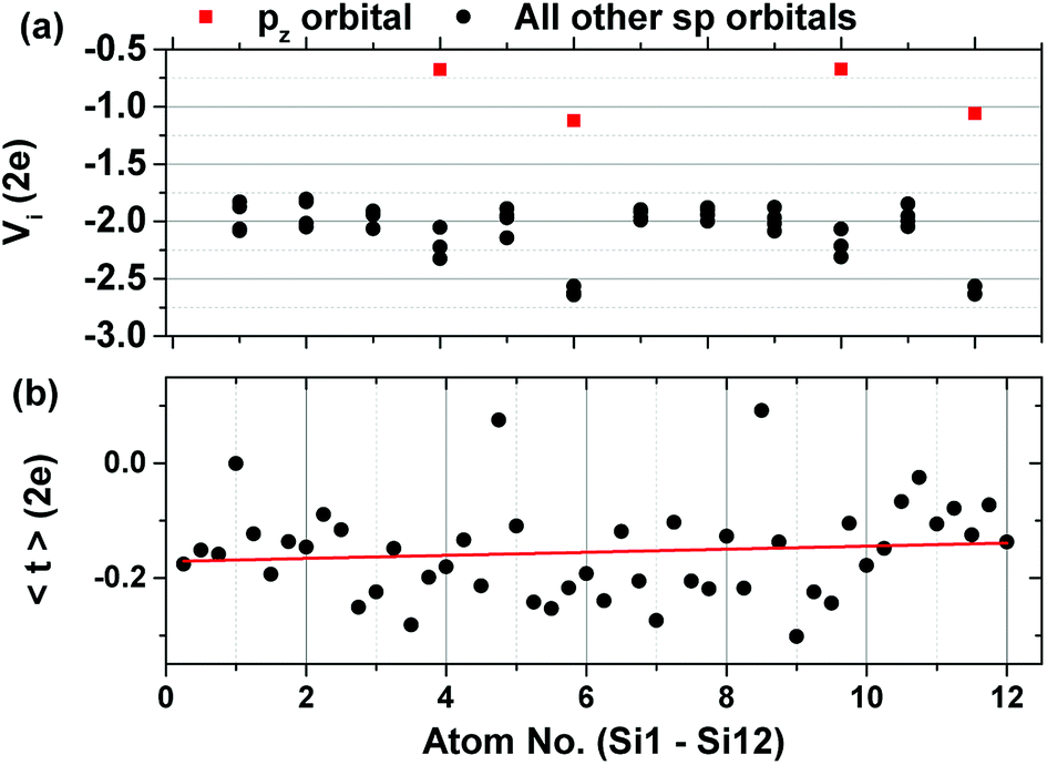 | ||
| Fig. 5 (a) On-site energies of the orbitals of each atom and (b) average value of the hopping integrals showing also a slight increase towards the top orbitals of the system. | ||
The TB Hamiltonian matrix resulting from the Wannierization is cut-off at three nearest neighbour hoppings. In this context, the nearest neighbours are the hoppings that lie within the home unit cell, second nearest neighbours are the hoppings to adjacent cells in all directions etc. The maximum order of the nearest neighbour interactions is dependent on the k-points used in the Monkhorst–pack mesh during the DFT calculations, as they define the number of periodic images that will appear when the system is translated in real space during Wannierization. As the number of nearest neighbours increases, a large number of neighbour interactions can significantly increase computation time both for creating the system and solving it. However, in most cases, three nearest neighbour interactions provide sufficient accuracy (see ESI†).
The conductance of the wire is calculated from the scattering matrix of the system.30 The dispersion relations within the leads that have 1D translational symmetry are shown together with the conductance plots in Fig. 6. The energies of the modes take on constant values in each direction due to the lack of a 3D translational symmetry. The magnitude of the conductance reflects the probability of transmission of the modes at each electrochemical potential difference between the leads. A value of two shows the there are two modes propagating in the wire at this energy etc.
 | ||
| Fig. 6 (a) Eigenenergies of the Hamiltonian of one unit cell in the lead, in the kx direction, with 3D translational symmetry (red lines) and similarly with 1D translational symmetry for 3 × 2 unit cells (black line) (b) quantum conductance of the wire in the same direction. | ||
Local charge and current densities are accessible through solving for individual or pairs of sites in the system, giving access to computations of many properties that exist at surfaces and interfaces. Fig. 7a shows the averaged local density of states from each orbital type which is taken from the expectation value of the local density operator in Kwant using,
 | (2) |
 | ||
| Fig. 7 (a) Local density of states for each orbital type in the quantum wire (b) orbital-projected DoS derived from DFT calculations using the PBE functional. | ||
At Ef −0.19 eV, an increased electron density is observed at Si7 sp3 and Si12 pz orbitals. To explain this, the expectation value of the current density at this energy was also extracted for the propagating wavefunctions originating from lead 1 (left lead in Fig. 4). For a hopping from site l to site k, this is calculated from,
 | (3) |
 | ||
| Fig. 8 (a) Vector plot showing the location of the hopping with the highest current density for each site. The colour scale shows the magnitude of the expectation value (2e h−1). The arrowhead shows the direction of the current at this hopping (b) interpolated current density and streamlines at two cuts perpendicular to kz at the vicinity of the highest concentration of local current density. Transport is in the kx direction (lead 1 towards lead 2). The locations of the atoms that exist at this z cut (with an approximate displacement of 1 Å) are marked in blue for the first four unit cells. Both results are taken at E = Ef – 0.19 eV. | ||
In the absence of any potential or magnetic field defined explicitly over the 3D region, the distribution of the current density is dictated by the confinement effects in the x, y and z directions,7 that is by the solution of the Schrodinger equation with the translation operator in the leads defining the energies of the propagating modes. Finally, the on-site energies as well as the hopping integral values define the electrostatic landscape for the electrons to find their route through the wire (Fig. 5).‡
Taking into account collective effects from many orbitals, the effects of impurities and screening or the formation of dipoles at interfaces41 can furthermore be examined, opening the road to versatile computational microscopic and topographic studies, while phonon effects can be added as site self-energies using standard procedures.8 Progress in obtaining and engineering model TB Hamiltonians from first principles is currently flourishing42 and is expected to lead to significant advances in predictions of device characteristics.
3 Conclusions
An ab initio multi-scale simulation approach has been presented for the calculation of the current density between adjacent atomic positions in a material using an effective Hamiltonian derived from Wannier functions. The methodology has been applied to a newly predicted material by the name bilayer penta-silicene, where we have observed an increased concentration of charge at specific orbitals in a free-standing quantum wire. This was found to be consistent with the expectation values of the DC local current between its atomic orbitals, which revealed the locations of the highest flow of charge.This methodology presents many advantages for the examination of electron device operation as it allows many microscopic details of the quantum transport to be revealed using realistic values and the addition of disorder, spin, phonon and finite-temperature effects. Bias calculations are also possible by summing the propagating modes around the Fermi level in the scattering region.43
4 Methods
DFT
Density functional theory calculations were performed using the Quantum Espresso package,44 norm-conserving Goedecker/Hartwigsen/Hutter/Teter pseudopotential with BLYP§ and PBE¶ exchange correlation functionals. 96 bands were included in the calculation for the 12 atoms of the unit cell, each with 4 valence electrons (3s2 3p2). The vacuum between periodic images in the z direction was set to 22 Å. The plane wave cut-off energy was set to 37 Ry and a Monkhorst–pack k-point mesh of 9 × 9 × 1 was used for the relaxation and the band structure calculations. These settings resulted in a lattice constant of 5.29 Å for the case of the BLYP and 5.21 Å for PBE.Wannier calculations
Wannier90 (ref. 37) calculations were performed with PBE functional DFT results given as input. A frozen window that included the 26 valence and 22 conduction bands was defined. The tolerance for the gauge invariant term of the spread of the WF was set to the really low value of 10−7 Å2 as the bands towards higher energies are highly entangled. The density of the k-point mesh was explicitly optimized to 15 × 15 × 1 k-points. Imaginary/real ratios of the order 10−3 to 10−4 were achieved for the WFs.Conflicts of interest
There are no conflicts to declare.Acknowledgements
This work was supported by computational resources granted from the Greek Research & Technology Network (GRNET) in the National HPC facility ‘ARIS’ under the project AMONADE (ID pr004002) and also used the European Grid Infrastructure (EGI) through the National Grid Infrastructures NGI GRNET, HellasGRID as part of the SEE Virtual Organisation. Data presented in this paper are available from DOI: 10.5281/zenodo.1438840.Notes and references
- L. Chen, J. Wen, P. Zhang, B. Yu, C. Chen, T. Ma, X. Lu, S. H. Kim and L. Qian, Nat. Commun., 2018, 9, 1542 CrossRef PubMed
.
- G. Hu, T. Albrow-Owen, X. Jin, A. Ali, Y. Hu, R. C. T. Howe, K. Shehzad, Z. Yang, X. Zhu, R. I. Woodward, T.-C. Wu, H. Jussila, J.-B. Wu, P. Peng, P.-H. Tan, Z. Sun, E. J. R. Kelleher, M. Zhang, Y. Xu and T. Hasan, Nat. Commun., 2017, 8, 278 CrossRef PubMed
- M. Trapatseli, A. Khiat, S. Cortese, A. Serb, D. Carta and T. Prodromakis, J. Appl. Phys., 2016, 120, 025108 CrossRef
- J. Fan, L. Jiang, S. Wang, R. Huang, K. A. Morgan, L. Zhong and C. H. de Groot, Microelectron. Eng., 2017, 174, 1–5 CrossRef CAS
- Y. Li, S. Long, Y. Liu, C. Hu, J. Teng, Q. Liu, H. Lv, J. Suñé and M. Liu, Nanoscale Res. Lett., 2015, 10(1), 420 CrossRef PubMed
- Y. Li, M. Zhang, S. Long, J. Teng, Q. Liu, H. Lv, E. Miranda, J. Suñé and M. Liu, Sci. Rep., 2017, 7, 1–11 CrossRef PubMed
- J. Wilhelm, M. Walz and F. Evers, Phys. Rev. B: Condens. Matter Mater. Phys., 2014, 89, 1–7 CrossRef
- D. K. Morr, Phys. Rev. B, 2017, 95, 1–5 CrossRef
- P. Willke, T. Druga, R. G. Ulbrich, M. A. Schneider and M. Wenderoth, Nat. Commun., 2015, 6, 1–5 Search PubMed
- F. Lüpke, M. Eschbach, T. Heider, M. Lanius, P. Schüffelgen, D. Rosenbach, N. Von Den Driesch, V. Cherepanov, G. Mussler, L. Plucinski, D. Grützmacher, C. M. Schneider and B. Voigtländer, Nat. Commun., 2017, 8, 1–7 CrossRef PubMed
- L. Tao, E. Cinquanta, D. Chiappe, C. Grazianetti, M. Fanciulli, M. Dubey, A. Molle and D. Akinwande, Nat. Nanotechnol., 2015, 10, 227–231 CrossRef CAS PubMed
- J. Zhao, H. Liu, Z. Yu, R. Quhe, S. Zhou, Y. Wang, C. C. Liu, H. Zhong, N. Han, J. Lu, Y. Yao and K. Wu, Prog. Mater. Sci., 2016, 83, 24–151 CrossRef CAS
- H. Şahin, S. Cahangirov, M. Topsakal, E. Bekaroglu, E. Akturk, R. T. Senger and S. Ciraci, Phys. Rev. B: Condens. Matter Mater. Phys., 2009, 80, 155453 CrossRef
- K. Chae, D. Y. Kim and Y.-W. Son, 2D Mater., 2018, 5, 025013 CrossRef
- Z. Zhuo, X. Wu and J. Yang, Nanoscale, 2018, 10, 1265–1271 RSC
- J. I. Cerdá, J. Sławińska, G. Le Lay, A. C. Marele, J. M. Gómez-Rodríguez and M. E. Dávila, Nat. Commun., 2016, 7, 13076 CrossRef PubMed
- S. Sheng, R. Ma, J. Wu, W. Li, L. Kong, X. Cong, D. Cao, W. Hu, J.-W. Luo and P. Cheng, et al., Nano Lett., 2018, 18(5), 2937–2942 CrossRef CAS PubMed
- Y. Aierken, O. Leenaerts and F. M. Peeters, Phys. Chem. Chem. Phys., 2016, 18, 18486–18492 RSC
- D. Logoteta, G. Fiori and G. Iannaccone, Sci. Rep., 2014, 4, 6607 CrossRef CAS PubMed
- H. Liu, G. Qin, Y. Lin and M. Hu, Nano Lett., 2016, 16, 3831–3842 CrossRef CAS PubMed
- P. Rivera, J. R. Schaibley, A. M. Jones, J. S. Ross, S. Wu, G. Aivazian, P. Klement, K. Seyler, G. Clark, N. J. Ghimire, J. Yan, D. G. Mandrus, W. Yao and X. Xu, Nat. Commun., 2015, 6, 6242 CrossRef CAS PubMed
- M.-H. Chiu, M.-Y. Li, W. Zhang, W.-T. Hsu, W.-H. Chang, M. Terrones, H. Terrones and L.-J. Li, ACS Nano, 2014, 8, 9649–9656 CrossRef CAS PubMed
- Y. Liu, N. O. Weiss, X. Duan, H.-C. Cheng, Y. Huang and D. Xiangfeng, Nat. Rev. Mater., 2016, 490, 16042 CrossRef
- I. Souza, N. Marzari and D. Vanderbilt, Phys. Rev. B: Condens. Matter Mater. Phys., 2001, 65, 035109 CrossRef
- K. S. Thygesen, L. B. Hansen and K. W. Jacobsen, Phys. Rev. Lett., 2005, 94, 026405 CrossRef CAS PubMed
- D. Gresch, G. Autès, O. V. Yazyev, M. Troyer, D. Vanderbilt, B. A. Bernevig and A. A. Soluyanov, Phys. Rev. B, 2017, 95, 1–24 CrossRef
- G. Pizzi, M. Gibertini, E. Dib, N. Marzari, G. Iannaccone and G. Fiori, Nat. Commun., 2016, 12585 CrossRef CAS PubMed
- G. Iannaccone, F. Bonaccorso, L. Colombo and G. Fiori, Nat. Nanotechnol., 2018, 13, 183–191 CrossRef CAS PubMed
- M. Walz, A. Bagrets and F. Evers, J. Chem. Theory Comput., 2015, 11, 5161–5176 CrossRef CAS PubMed
- C. W. Groth, M. Wimmer, A. R. Akhmerov and X. Waintal, New J. Phys., 2014, 16, 063065 CrossRef
- J. R. Schaibley, H. Yu, G. Clark, P. Rivera, J. S. Ross, K. L. Seyler, W. Yao and X. Xu, Nat. Rev. Mater., 2016, 1, 16055 CrossRef CAS
- J. Weston and X. Waintal, J. Comput. Electron., 2016, 4, 1148–1157 CrossRef
- G. Fiori and G. Iannaccone, Proc. IEEE, 2013, 101(7), 1653–1669 CAS
- Y. Ding and Y. Wang, Appl. Phys. Lett., 2013, 102, 143115 CrossRef
- Y. Ding and Y. Wang, Appl. Phys. Lett., 2014, 104, 083111 CrossRef
- P. Löwdin, J. Chem. Phys., 1950, 18, 365–375 CrossRef
- A. A. Mostofi, J. R. Yates, G. Pizzi, Y.-S. Lee, I. Souza, D. Vanderbilt and N. Marzari, Comput. Phys. Commun., 2014, 2309 CrossRef CAS
- D. Gresch, TBmodels Documentation, 2016, https://z2pack.ethz.ch/tbmodels Search PubMed
- N. Marzari, A. A. Mostofi, J. R. Yates, I. Souza and D. Vanderbilt, Rev. Mod. Phys., 2012, 84, 1419–1475 CrossRef CAS
- D. Gresch, Q. Wu, G. W. Winkler, R. Häuselmann, M. Troyer and A. A. Soluyanov, 2018, arXiv preprint arXiv:1805.12148.
- I. Salaoru, S. Alotaibi, Z. Al Halafi and S. Paul, MRS Adv., 2017, 2, 195–208 CrossRef CAS
- S. Coh and D. Vanderbilt, Python Tight Binding (PythTB), 2016, https://www.physics.rutgers.edu/pythtb/index.html Search PubMed
- L. E. Foa Torres, V. Dal Lago and E. Suárez Morell, Phys. Rev. B, 2016, 93, 1–7 CrossRef
- P. Giannozzi, O. Andreussi, T. Brumme, O. Bunau, M. B. Nardelli, M. Calandra, R. Car, C. Cavazzoni, D. Ceresoli, M. Cococcioni, N. Colonna, I. Carnimeo, A. D. Corso, S. de Gironcoli, P. Delugas, R. A. D. Jr, A. Ferretti, A. Floris, G. Fratesi, G. Fugallo, R. Gebauer, U. Gerstmann, F. Giustino, T. Gorni, J. Jia, M. Kawamura, H.-Y. Ko, A. Kokalj, E. Kucukbenli, M. Lazzeri, M. Marsili, N. Marzari, F. Mauri, N. L. Nguyen, H.-V. Nguyen, A. O. de-la Roza, L. Paulatto, S. Poncé, D. Rocca, R. Sabatini, B. Santra, M. Schlipf, A. P. Seitsonen, A. Smogunov, I. Timrov, T. Thonhauser, P. Umari, N. Vast, X. Wu and S. Baroni, J. Phys.: Condens. Matter, 2017, 29, 465901 CrossRef CAS PubMed
Footnotes |
| † Electronic supplementary information (ESI) available. See DOI: 10.1039/c8ra05652h |
| ‡ While writing this manuscript the authors were made aware of another work that adds to the Wannierization procedure by creating symmetrized tight binding models.40 This is expected to significantly increase the accuracy of the ideal ground state model Hamiltonian. |
| § http://www.quantum-espresso.org/wp-content/uploads/upf_files/Si.blyp-hgh.UPFhttp://www.quantum-espresso.org/wp-content/uploads/upf_files/Si.blyp-hgh.UPF |
| ¶ http://www.quantum-espresso.org/wp-content/uploads/upf_files/Si.pbe-hgh.UPFhttp://www.quantum-espresso.org/wp-content/uploads/upf_files/Si.pbe-hgh.UPF |
| This journal is © The Royal Society of Chemistry 2018 |