DOI:
10.1039/C8RA05479G
(Paper)
RSC Adv., 2018,
8, 28953-28959
Enhanced visible transmittance and reduced transition temperature for VO2 thin films modulated by index-tunable SiO2 anti-reflection coatings
Received
26th June 2018
, Accepted 9th August 2018
First published on 14th August 2018
Abstract
The low visible transmission is one of the bottleneck problems for the application of vanadium dioxide films since the high refractive index (RI) of VO2 films results in strong reflection in the visible wavelength. To address this problem, in this paper, high-purity VO2 films were deposited on fused silica by DC reactive magnetron sputtering at low temperature of 320 °C. Silica sol–gel coatings with tunable refractive index (RI) coated onto VO2 films have been fabricated to enhance visible transmittance with the potential application in the field of smart windows. SiO2 coatings with tunable RI (1.16–1.42 at λ = 700 nm) were prepared by sol–gel dip-coating technique. The double structure SiO2/VO2 films were characterized through several techniques, including X-ray diffraction, UV-VIS-NIR spectrophotometry and scanning electron microscopy. Compared with the single-layer VO2 film (ΔTsol of 6.25% and Tlum of 38.58%), the three kinds of SiO2/VO2 bilayer films had higher Tlum (41.93–50.44%) and larger ΔTsol (8.15–8.51%) simultaneously due to significantly decreased reflectance. Moreover, the crystallization properties of VO2 films are essentially unchanged by applying a SiO2 top layer, while the phase transition temperature and thermal hysteresis width of sample S116 are lower than those of pure VO2 film. The presented RI-tunable SiO2 coatings, can regulate optical properties continuously for various VO2 substrates, paving the way for practical applications of VO2 films in the field of smart windows or others.
1. Introduction
Vanadium dioxide (VO2) is the best thermochromic material for energy-efficient smart windows.1,2 At the critical temperature (∼68 °C), a reversible semiconductor-to-metal transition occurs in bulk VO2.3 Accompanied with the crystal structure transitioning from rutile phase (R) to monoclinic phase (M), VO2 exhibits a drastic change in electrical conductivity and NIR optical transmittance.4 Such specific features make VO2 a potential candidate in the application of thermochromic energy-efficient smart windows, uncooled infrared (IR) microbolometers, laser protection and optical storage devices.5–8 High-purity VO2 films can be fabricated by many preparation methods, including the pulsed laser deposition, sol–gel method, chemical vapor deposition (CVD), thermal evaporation, atomic layer deposition and magnetron sputtering.9–14 Among these, magnetron sputtering technology shows great advantages for the application of VO2 films in smart windows due to the good uniformity and potential for industrialization.15
Up till now, there has been no successful application of vanadium dioxide in the field of smart windows. To realize an available solution, several challenges needed to be overcame: low solar modulating ability, unattractive color, high transition temperature and especially low visible transmittance. Generally, the low transmission of single 80 nm VO2 film can only reach 40% in the visible region (380–780 nm).16 There have been various popular methods to enhance the visible transmittance of VO2 films: metal-ion doping,17 multilayer structure,18 porous texture,19 etc. Moreover, VO2 films with different nanostructures can behaver enhanced Tlum and ΔTsol, such as moth eye structure,20 photonic structure,21 plasmonic structure22 and grided structure23. Additionally, applying antireflection coatings (ARCs) on the film surface can also be a promising approach to improve the visible transmittance of VO2 films through TiO2, ZnO, ZrO2 or SiO2, etc.,24 which is useful in industrial applications. The anti-reflective devise of double-layer films should be enhanced as the high RI and reflectivity of VO2 films in the visible region. However, most of the overcoats are usually with high RI, expensive and energy-consuming. It is worth noting that compared with other antireflection coatings, the SiO2 coatings with low RI prepared by low-cost sol–gel methods behaved some advantages of large-area, widespread used and anti-oxidation.25,26 Much research has been devoted to the fabrication of SiO2/VO2 double-layer structure to improve the visible transmission of VO2 films significantly. Yu et al. increased the Tlum of VO2 film from 37.6% to 47.7% via SiO2/VO2 composite structure, while ΔTsol exhibited an obvious decrease trend from 8.06% to 7.62%.27 Zhang et al. introduced SiO2 with RI of 1.299 as an antireflection coating coated on the VO2 film, which improved the visible transmission from 69.8% to 80.0% significantly, whereas the NIR control capability was also slightly decreased from 12.6% to 10.2%.28
Therefore, in this study, SiO2 anti-reflection coatings with tunable refraction index were coated on VO2 films to enhance ΔTsol and Tlum simultaneously and continuously. Furthermore, the RI tunability of top SiO2 coatings can be applied to not only the VO2 continuous thin films but also the nanocomposites and micro-patterned VO2 films to improve the nanothermochromism effect.29 In addition, an anti-oxidation overcoat is also necessary for the unstable VO2 films. Index-tunable anti-reflection SiO2 coatings optimized by sol–gel method prepared on the surface of VO2 films by sol–gel dip-coating technique. The effect of RI tunability of SiO2 coatings on the thermochromism and optical properties of VO2 films was investigated.
2. Experimental details
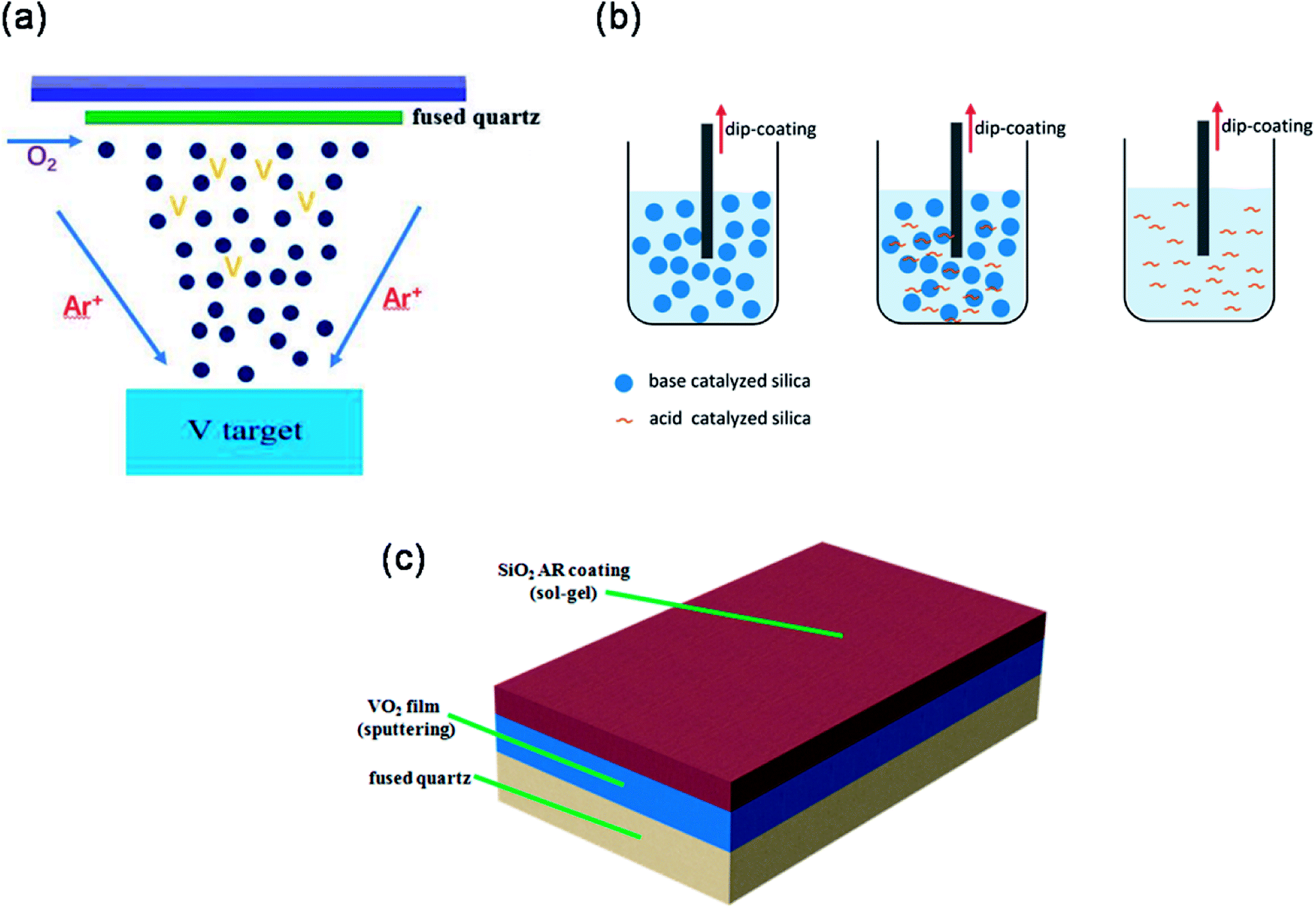
VO2 films were deposited on the fused silica by reactive magnetron sputtering technique. The deposition chamber was pumped to a base pressure of 4 × 10⁻⁴ Pa by using a turbo molecular pump, and pre-cleaned in Ar gases for 10 min to remove contamination from the target surface. The vanadium target (Φ60 mm) of purity 99.999% was used and the power density of V target was 4.2 W cm−2. The distance of target-substrate was approximately 100 mm. Pure oxygen gas and argon gas were introduced to chamber at 1.8 sccm and 40 sccm, respectively. The deposition pressure and substrate temperature were maintained at 0.5 Pa and 320 °C, respectively. The deposition time was 30 min and the thickness of VO2 films was controlled accurately to 150 nm. A schematic of DC magnetron sputtering is shown in Fig. 1(a). For low refractive silica (n = 1.16), the SiO2 sols were prepared by base catalysis of ammonia, mixed with the teraethoxysilane (TEOS), H2O, NH3 and ethanol (C2H5OH). The molar ratio of TEOS, H2O, C2H5OH and NH3 was 1![[thin space (1/6-em)]](https://www.rsc.org/images/entities/char_2009.gif) :2:34.2:0.9.30 High refractive silica (n = 1.42) was synthesized by mixing teraethoxysilane (TEOS), H2O, HCl and ethanol (C2H5OH). The molar ratio of TEOS, H2O, C2H5OH and HCl was 1:4:20:0.05.31 The SiO2 coating with refractive index of 1.34 was prepared by mixing low refractive silica and high refractive silica with a molar ratio of 7:3.
:2:34.2:0.9.30 High refractive silica (n = 1.42) was synthesized by mixing teraethoxysilane (TEOS), H2O, HCl and ethanol (C2H5OH). The molar ratio of TEOS, H2O, C2H5OH and HCl was 1:4:20:0.05.31 The SiO2 coating with refractive index of 1.34 was prepared by mixing low refractive silica and high refractive silica with a molar ratio of 7:3.
 |
| | Fig. 1 Schematic diagrams of procedure of preparation of (a) VO2 films and (b) SiO2 sols. (c) Schematic illustration of the structure of SiO2/VO2 double-layer film. | |
The above resulting chemical reagents were stirred for 5 h and placed into an oven to age for 4 days. VO2 films (Φ30 mm, d = 3 mm) were coated with the three kinds of silicas by a dip coating process with a withdrawal speed of 7 cm min−1, and then were baked at 180 °C for 24 h. The thickness of SiO2 antireflection coating was about 110 nm. The schematics of preparation process of SiO2 sols and dip coating process are shown Fig. 1(b). The SiO2/VO2 bilayer films coated by SiO2 coatings with refractive indices of 1.16, 1.34 and 1.42 are denoted as S116, S134 and S142, respectively. And the VO2 film without SiO2 antireflection is marked as PVO2. Fig. 1(c) illustrates the structure of VO2 film on fused quartz with a SiO2 antireflection coating. The optical transmittance of the SiO2/VO2 bilayer films were studied with a PerkinElmer Lambda 950 UV-VIS-NIR spectrophotometer from 250 to 2500 nm. A spectroscopic ellipsometer (Horiba uvisel 2) was used to characterize the refractive indices and physics thickness of SiO2 coatings. The microstructure characterization of pure VO2 and SiO2/VO2 bilayer films was measured by X-ray diffraction (Rigaku Ultima IV) with a 2θ geometry. In addition, the optical transition behavior was studied by Thin film phase transition measurement system (PERFECT PTM1700) to collect the IR transmittance of films at a fixed wavelength (1550 nm) against temperature with an interval of 1.0 °C. The surface morphologies of the films were observed using a field-emission scanning electron microscope (Zeiss Supra 5S). The calculation of integral visible transmittance (Tlum, 380–780 nm) and solar transmittance (Tsol, 250–2500 nm) can refer to our previous work.16
3. Results and discussion
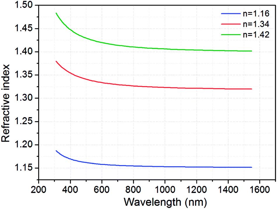
The refractive index of SiO2 films with wavelength were measured by using ellipsometry and fitted by Cauchy ellipsometry model. Fig. 2 shows the refractive indices of SiO2 antireflection coatings dipped by base catalyzed silica, acid catalyzed silica and mixed of them on the fused quartz. The refractive index of the SiO2 film prepared by base catalyzed silica was measured to be ∼1.16 at 700 nm, considerably lower than that prepared by acid catalyzed silica (∼1.42) or that prepared by mixed of base and acid catalyzed silica (∼1.34). On the other hand, the wavelength dispersions of the refractive index and extinction coefficient of pure VO2 films below and above phase transition temperature were also measured and fitted by ellipsometry, which can be found from our previous work.5
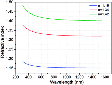 |
| | Fig. 2 Dispersion curves of the refractive indices of the SiO2 AR coatings prepared on the fused quartz. | |
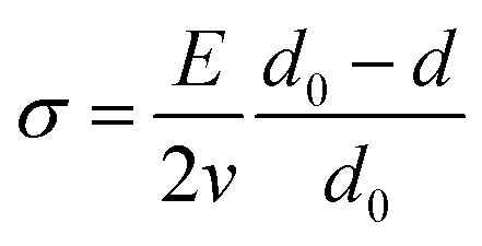
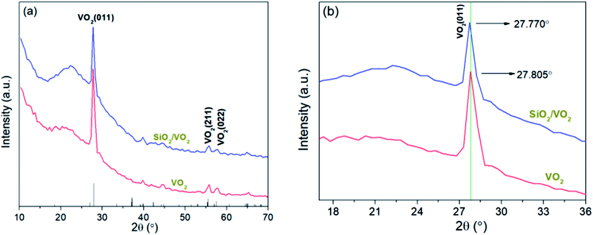
Fig. 3(a) shows the XRD patterns of both bottom-layer and double-layer thin films on quartz substrates, including the standard pattern of monoclinic (M) VO2 (PDF#82-0661). All the diffraction peaks of bottom-layer and double-layer films are similar, which correspond with the characteristic pattern of the VO2 M-phase. It is worth noting that no other impurity peaks (such as V2O3, V2O5 or V4O9) can be observed in the XRD patterns, indicating the formation of high-purity single crystal VO2 films. These reveal that high-quality VO2 films were obtained through DC reactive magnetron sputtering at low substrate temperature and the crystalline of VO2 in double-layer film was unchanged after coated with sol–gel silica anti-reflection coatings. Additionally, the broad peaks in the range of 10° to 25° were assigned to fused quartz substrates. The fine patterns of VO2 (011) peaks is shown in Fig. 3(b). It can be obvious seen that the values of two film samples are both slightly smaller than 27.827° of VO2 powder diffraction, and the value of intense diffraction peak position of the double-layer SiO2/VO2 film sample is slightly smaller than 27.805° of the pure VO2 film sample. The stress in films could be calculated by the formula:15
| |
 | (1) |
where
d and
d0 are the lattice distances in the strained and unstrained states, respectively.
E and
v are Young's modulus and Poisson's ratio of the film, respectively. The lattice coefficient could be obtained according to Bragg formula:
| | |
2dsinθ = kλ
| (2) |
where
θ is the X-ray diffraction angle, and
λ is the X-ray wavelength. The compressive stress in double-layer SiO
2/VO
2 film sample is larger than that of pure VO
2 film after calculation from the above formulas.
 |
| | Fig. 3 XRD spectra of the pure VO2 film and SiO2/VO2 film: (a) normalized patterns; (b) fine patterns of VO2 (011) peaks. | |
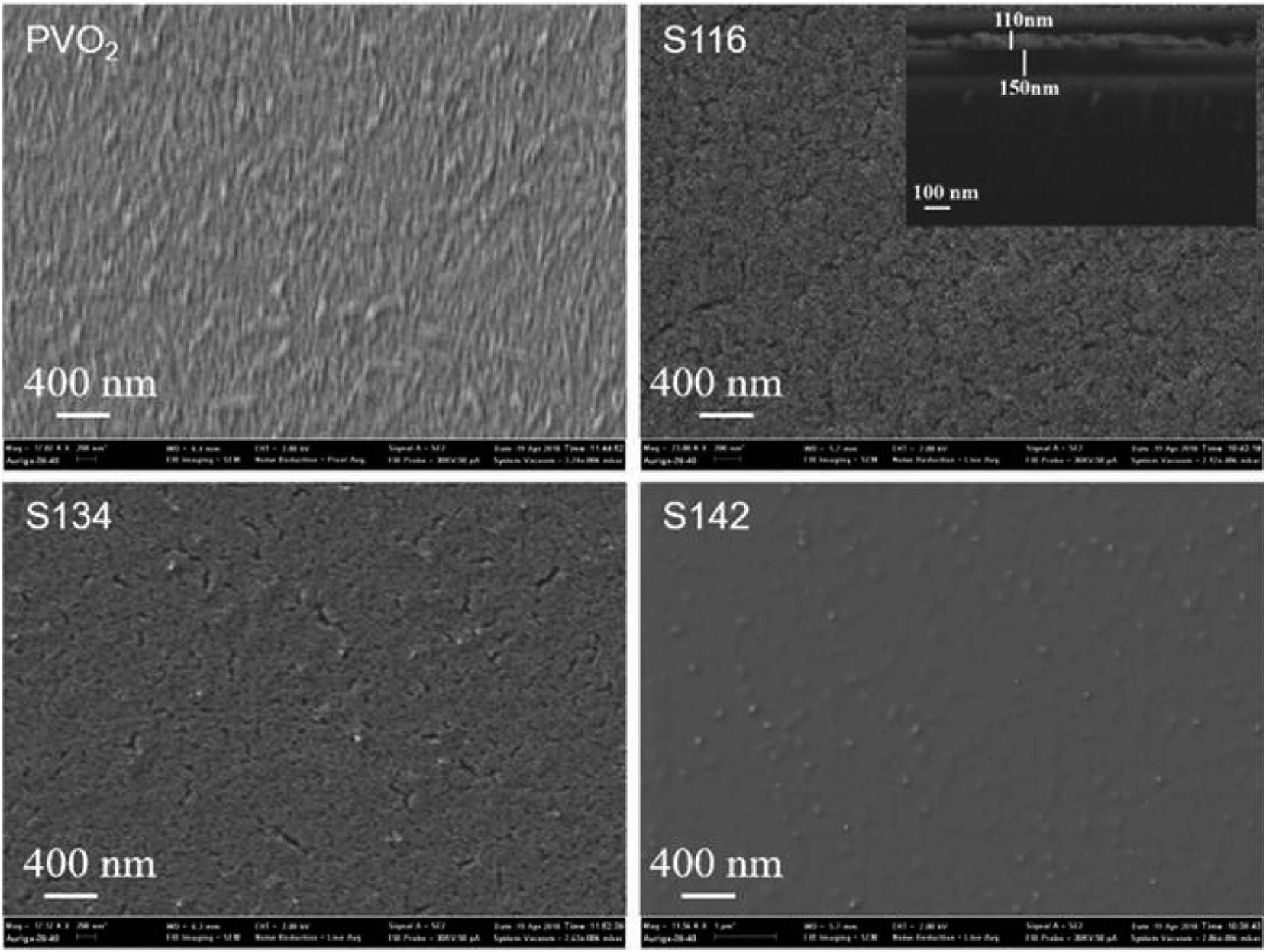
Fig. 4 shows the top-view SEM images of pure VO2 and SiO2/VO2 bilayer films. For the pure VO2 film, rice-like nanoparticles scattered on the surface, indicating the good crystallinity of the sample. The morphology is porous for the sample S116, while the sample S142 behaved a denser structure without any pores on the surface. The surface morphology of sample S134 shows both characteristic mentioned above. Moreover, the cross-sectional SEM image of sample S116 is shown in the inset image of Fig. 4, in which an obvious interface between the 110 nm SiO2 antireflective layer and 150 nm VO2 film can be observed.
 |
| | Fig. 4 Top-view SEM images of pure VO2 and SiO2/VO2 bilayer films. | |
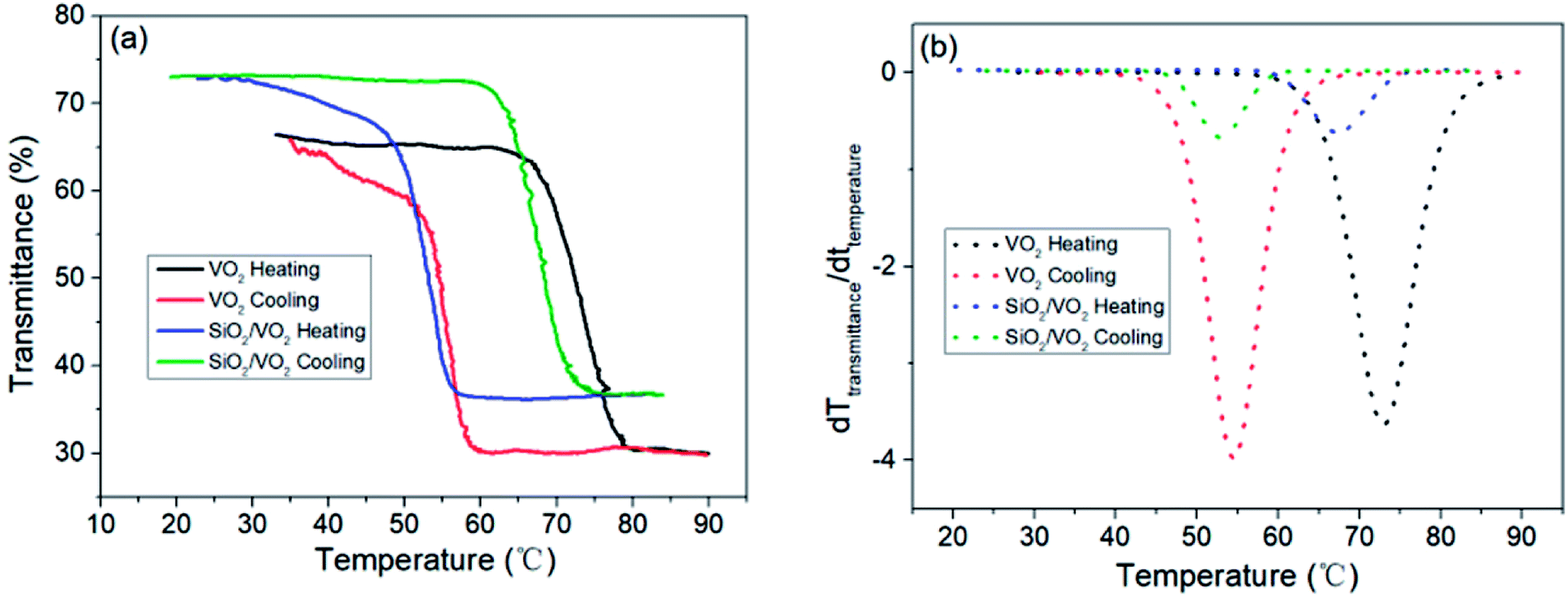
Fig. 5(a) shows the temperature-dependent transmittance of the pure VO2 film and S116 bilayer film sample at λ = 1550 nm. Thermal hysteresis loop is evident for both film samples and the semiconductor-to-metal transition occurred, indicating that the double-layer SiO2/VO2 film sample maintained the phase transition properties. Compared with the pure VO2 film, the enhancement of transmittance at λ = 1550 nm is obvious, and the highest value can reach 72% for the sample S116. The tunable-RI SiO2 coatings can significantly suppress the optical reflection losses and improve light transmission.
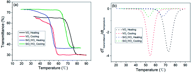 |
| | Fig. 5 (a) Transmittance hysteresis loops of pure VO2 film and SiO2/VO2 bilayer films at λ = 1550 nm and (b) corresponding dT/dt vs. temperature curve for film samples PVO2 and S116. | |
Fig. 5(b) shows the Standard Gauss fitting derivative logarithmic plots, which were obtained by taking the derivative of the logarithmic transmittance with respect to the temperature of film sample. Phase transition temperature can be defined as Tc = (Tl + Th)/2, and the thermal hysteresis width was calculated by ΔH = Th − Tl. The values of phase transition temperatures for pure VO2 and S116 film sample are 63.5 °C and 60 °C, respectively, which are lower than 68 °C of the bulk VO2. Moreover, the phase transition temperature of sample S116 is lower than that of pure VO2 film. The main reason is that the larger compressive stress existed in the double-layer film sample compared with the pure VO2 film sample, which has been discussed in the XRD analysis. Our previous work32 reported that the compressive stress changed the phase transition temperature of VO2 film samples by applying TiO2 buffer layers. The width of the hysteresis loop of sample S116 is 14.5 °C, which is also smaller than that of pure VO2 film sample (18.5 °C). These results are different from other reports, which usually revealed that adding SiO2 antireflection coatings would increase the Tc and ΔH to a certain extent due to the existence of SiO2 as thermal insulation.24,28 The main reason of our experimental results may be the special porous morphology for the sample S116 with low refractive index.
To investigate the effect of RI-fixed SiO2 coatings on the optical properties of the VO2 films, the transmittance spectra were examined as shown in Fig. 6(a). The visible transmittance (at λ = 700 nm) and IR transmittance modulation (at λ = 2500 nm) of the film samples were calculated, as shown in Fig. 6(b). The transmittance at λ = 700 nm for the samples with SiO2 antireflection coatings is higher than that of the single-layer VO2 film, in which the sample with SiO2 refractive index of 1.42 behaved the best. The visible transmittance at λ = 700 nm increased from 47% to 66% as the refractive index of SiO2 antireflection coating increased from 1.16 to 1.42.
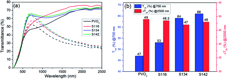 |
| | Fig. 6 (a)Transmittance spectra of pure VO2 film and bilayer films. Solid lines represent the transmittance recorded at 25 °C and dotted lines measured at 80 °C. (b) Tvis at λ = 700 nm and ΔTIR at λ = 2500 nm for the samples. | |
To fully display the superior optical properties of single-layer VO2 and SiO2/VO2 double-layer films, the luminous transmittance (Tlum) and solar spectral transmittance (Tsol) of film samples were calculated based on the measured transmittance using the following eqn (3) and (4):
| |
 | (3) |
| |
 | (4) |
here,
T(
λ) represents the transmittance,
φsol is the solar spectral irradiance for mass of 1.5. The angle between the sun and the horizon is above 37° and the wavelength is 280–2500 nm.
φlum is the standard luminous efficiency function of photonic vision and the wavelength for the
φlum is 380–780 nm. The values of Δ
Tsol and
Tlum(avg) can be obtained as follows:
| | |
ΔTsol = Tsol,l − Tsol,h
| (5) |
| | |
Tlum(avg) = (Tlum,l + Tlum,h)/2
| (6) |
here,
Tsol,l indicates the solar transmittance in semiconductor state and
Tsol,h indicates the solar transmittance in metal state.
Tlum,l and
Tlum,h mean the luminous transmittance in the low temperature state and high temperature state, respectively.
The solar switching efficiency (ΔTsol) and visible transmittance (Tlum) of the pure VO2 film and bilayer films are shown on Table 1. It is obvious that Tlum and ΔTsol of the SiO2/VO2 films were all higher than the pure VO2 film. Furthermore, the Tlum,l and Tlum,h of these samples both increased obviously as the refractive indices of SiO2 coatings increased from 1.16 to 1.42, and the values of ΔTsol also exhibited a slightly increasing trend at the same time. The maximum values of Tlum and ΔTsol for film sample S142 can reach 50.44% and 8.51%, respectively. This result was better than the values of reported VO2@SiO2 arrays prepared by rapid thermal annealing of sputtered vanadium films,26 SiO2/VO2 double-layered films obtained vis plasma enhanced chemical vapor deposition,27 α-SiO2/VO2/α-SiO2 multi-layered films and TiO2/VO2 films deposited by radio frequency reactive magnetron sputtering.33,34 Although the TiO2(R)/VO2(M)/TiO2(A)35 multi-layered films made through radio frequency reactive magnetron sputtering and VO2/SiO2/TiO2 (ref. 36) films fabricated vis atmospheric-pressure chemical vapor deposition behaved higher ΔTsol than our result, the values of their Tlum(avg) were lower. More detailed results about recent studies were summarized in Table 1. In this work, the formation of smoother and denser film surface after SiO2 coating can decrease the light scattering of the sample and enhance the visible transmittance. These results indicate that applying SiO2 antireflection coatings with tunable refraction index can be an efficient way to enhance the visible transmittance of VO2 films simultaneously and continuously.
Table 1 Solar switching efficiency (ΔTsol) and luminous transmittance (Tlum) of the pure VO2 film and SiO2/VO2 bilayer films compared with the reported studies
| Samples |
Tsol,l [%] |
Tsol,h [%] |
ΔTsol [%] |
Tlum,l [%] |
Tlum,h [%] |
Tlum(avg) [%] |
ΔTlum [%] |
| PVO2 (this work) |
44.57 |
38.32 |
6.25 |
37.06 |
40.10 |
38.58 |
3.04 |
| S116 (this work) |
50.71 |
42.43 |
8.28 |
40.81 |
43.04 |
41.93 |
2.23 |
| S134 (this work) |
54.14 |
45.99 |
8.15 |
47.77 |
48.37 |
48.07 |
0.60 |
| S142 (this work) |
57.83 |
49.32 |
8.51 |
50.11 |
50.76 |
50.44 |
0.65 |
| VO2@SiO2 arrays26 |
— |
— |
6.70 |
— |
— |
43.50 |
— |
| SiO2/VO2 (ref. 27) |
— |
— |
7.62 |
— |
— |
47.70 |
— |
| α-SiO2/VO2/α-SiO2 (ref. 33) |
36.50 |
32.00 |
4.50 |
35.20 |
34.80 |
35.00 |
0.40 |
| TiO2/VO2 (ref. 34) |
46.25 |
39.26 |
6.99 |
49.15 |
45.05 |
47.10 |
4.10 |
| TiO2(R)/VO2(M)/TiO2(A)35 |
33.80 |
23.60 |
10.20 |
30.10 |
27.80 |
28.95 |
2.30 |
| Moth-eye structure20 |
52.10 |
45.00 |
7.10 |
43.60 |
45.30 |
44.50 |
−1.70 |
| VO2/SiO2/TiO2 coating36 |
28.83 |
13.55 |
15.29 |
17.81 |
18.23 |
18.02 |
−0.42 |
4. Conclusion
In this work, SiO2/VO2 bilayer films were synthesized successfully by magnetron sputtering and sol–gel method. The crystallization properties of VO2 films is essentially unchanged by applying SiO2 top layer. The bilayer films can behave high transmittance and good thermochromic performance when compared with the single-layer pure VO2 film. For the sample S142, the maximum value of Tlum can reach 50.44%. For the sample S116, the width of hysteresis loop and transition temperature are 14.5 °C and 60 °C, respectively, which are smaller than those of pure VO2 film sample (18.5 °C and 63.5 °C). Moreover, the Tlum of these bilayer films increased obviously as the refractive index of SiO2 antireflective layer increased from 1.16 to 1.42, and the ΔTsol exhibited a slightly increasing trend. Hence, the enhancement of Tlum and ΔTsol simultaneously and continuously provides a meaningful solution for VO2-based thermochromic energy-efficient smart windows.
Conflicts of interest
There are no conflicts to declare.
Acknowledgements
This work was supported by the Shenzhen Science & Technology Project (JCYJ20150529164656098, ZDSY20170228105421966), National Nature Science Foundation of China (Grant No. 11705259) and the Research & Development Fund of Guangdong/ Shenzhen (2016B090930011, JCYJ20160226192609015).
References
- Z. Y. Cao, Y. Lu, X. D. Xiao, Y. J. Zhan, H. L. Cheng and G. Xu, Mater. Lett., 2017, 209, 609–612 CrossRef.
- J. B. Kana Kana, G. Vignaud, A. Gibaud and M. Maaza, Opt. Mater., 2016, 54, 165–169 CrossRef.
- L. L. Fan, X. Q. Wang, F. Wang, Q. F. Zhang, L. Zhu, Q. Q. Meng, B. l. Wang, Z. M. Zhang and C. W. Zou, RSC Adv., 2018, 8, 19151–19156 RSC.
- H. Y. Xu, Y. H. Huang, S. Liu, K. W. Xu, F. Ma and P. K. Chu, RSC Adv., 2016, 6, 79383–79388 RSC.
- D. P. Zhang, M. D. Zhu, Y. Liu, K. Yang, G. X. Liang, Z. H. H. Zheng and X. M. Cai, J. Alloys Compd., 2016, 659, 198–202 CrossRef.
- S. Chen, L. Dai, J. J. Liu, Y. F. Gao, X. L. Liu, Z. Chen, J. D. Zhou, C. X. Cao, P. G. Han, H. J. Luo and M. Kanahira, Phys. Chem. Chem. Phys., 2013, 15, 17537 RSC.
- S. H. Chen, H. Ma, X. J. Yi, T. Xiong, H. C. Wang and C. J. Ke, Sens. Actuators, A, 2004, 115, 28–31 CrossRef.
- G. V. Jorgenson and J. C. Lee, Sol. Energy Mater., 1986, 14, 205 CrossRef.
- J. Wu, W. X. Huang, Q. W. Shi, J. H. Cai, D. Zhao, Y. B. Zhang and J. Z. Yan, Appl. Surf. Sci., 2013, 268, 556–560 CrossRef.
- K. Martens, I. P. Radu, S. Mertens, X. Shi, L. Nyns, S. Cosemans, P. Favia, H. Bender, T. Conard, M. Schaekers, S. De Gendt, V. Afanas'ev, J. A. Kittl, M. Heyns and M. Jurczak, J. Appl. Phys., 2012, 112, 124501 CrossRef.
- V. Thery, A. Boulle, A. Crunteanu, J. C. Orlianges, A. Beaumont, R. Mayet, A. Mennai, F. Cosset, A. Bessaudou and M. Fabert, J. Appl. Phys., 2017, 121, 055303 CrossRef.
- D. Vernardou, D. Louloudakis, E. Spanakis, N. Katsarakis and E. Koudoumas, Sol. Energy Mater. Sol. Cells, 2014, 128, 36–40 CrossRef.
- J. Sakai, M. Zaghrioui, V. T. Phuoc, S. Roger, C. Autret-Lambert and K. Okimura, J. Appl. Phys., 2013, 113, 123503 CrossRef.
- Y. Huang, D. P. Zhang, Y. Liu, J. C. Jin, Y. Yang, T. Chen, H. Guan, P. Fan and W. Z. Lv, Appl. Surf. Sci., 2018, 456, 545–551 CrossRef.
- M. D. Zhu, H. J. Qi, C. Li, B. Wang, H. Wang, T. R. Guan and D. P. Zhang, Appl. Surf. Sci., 2018, 453, 23–30 CrossRef.
- M. D. Zhu, H. J. Qi, B. Wang, H. Wang, T. R. Guan and D. P. Zhang, J. Alloys Compd., 2018, 740, 844–851 CrossRef.
- J. D. Zhou, Y. F. Gao, X. L. Liu, Z. Chen, L. Dai, C. X. Cao, H. J. Luo, M. Kanahira, C. Sun and L. M. Yan, Phys. Chem. Chem. Phys., 2013, 15, 7505 RSC.
- N. R. Mlyuka, G. A. Niklasson and C. G. Granqvist, Sol. Energy Mater. Sol. Cells, 2009, 93, 1685–1687 CrossRef.
- L. T. Kang, Y. F. Gao, H. J. Luo, Z. Chen, J. Du and Z. T. Zhang, ACS Appl. Mater. Interfaces, 2011, 3, 135–138 CrossRef PubMed.
- X. K. Qian, N. Wang, Y. F. Li, J. H. Zhang, Z. C. Xu and Y. Long, Langmuir, 2014, 30, 10766–10771 CrossRef PubMed.
- Y. Ke, I. Balin, N. Wang, Q. Lu, A. I. Y. Tok, T. J. White, S. Magdassi, I. Abdulhalim and Y. Long, ACS Appl. Mater. Interfaces, 2016, 8, 33112–33120 CrossRef PubMed.
- Y. J. Ke, X. L. Wen, D. Y. Zhao, R. C. Che, Q. H. Xiong and Y. Long, ACS Nano, 2017, 11, 7542–7551 CrossRef PubMed.
- C. Liu, Y. Long, S. Magdassi and D. Mandler, Nanoscale, 2017, 9, 485 RSC.
- C. Wang, L. Zhao, Z. Liang, B. Dong, L. Wan and S. Wang, Sci. Technol. Adv. Mater., 2017, 18, 563–573 CrossRef PubMed.
- D. Li, Y. Shan, F. Huang and S. Ding, Appl. Surf. Sci., 2014, 317, 160–166 CrossRef.
- L. W. Zhou, J. R. Liang, M. Hu, P. Li, X. L. Song, Y. R. Zhao and X. Y. Qiang, Appl. Phys. Lett., 2017, 110, 193901 CrossRef.
- J. H. Yu, S. H. Nam, J. W. Lee and J. H. Boo, Materials, 2016, 9, 556 CrossRef PubMed.
- J. Zhang, J. Wang, C. M. Yang, H. B. Jia, X. M. Cui and S. C. Zhao, Sol. Energy Mater. Sol. Cells, 2017, 162, 134–141 CrossRef.
- C. Liu, S. C. Wang, Y. Zhou, H. B. Yang, Q. Lu, D. Mandler, S. Magdassi, C. Y. Tay and Y. Long, J. Alloys Compd., 2018, 731, 1197–1207 CrossRef.
- B. Shen, H. Y. Li, H. Xiong, X. Zhang and Y. X. Tang, Chin. Opt. Lett., 2016, 14, 083101 CrossRef.
- Q. Jia, Acta Opt. Sin., 2004, 24, 65 Search PubMed.
- D. P. Zhang, K. Yang, Y. Li, Y. Liu, M. D. Zhu, A. H. Zhong, X. M. Cai, P. Fan and W. Z. Lv, J. Alloys Compd., 2016, 684, 719–725 CrossRef.
- H. Kakiuchida, P. Jin and M. Tazawa, Sol. Energy Mater. Sol. Cells, 2008, 92, 1279–1284 CrossRef.
- P. Jin, G. Xu, M. Tazawa and K. Yoshimura, Jpn. J. Appl. Phys., 2002, 41, L278–L280 CrossRef.
- J. Zheng, S. Bao and P. Jin, Nano Energy, 2015, 11, 136–145 CrossRef.
- M. J. Powell, R. Quesada-Cabrera, A. Taylor, D. Teixeira, I. Papakonstantinou, R. G. Palgrave, G. Sankar and I. P. Parkin, Chem. Mater., 2016, 28, 1369–1376 CrossRef.
|
| This journal is © The Royal Society of Chemistry 2018 |
Click here to see how this site uses Cookies. View our privacy policy here. 
 Open Access Article
 This Open Access Article is licensed under a Creative Commons Attribution-Non Commercial 3.0 Unported Licence
 ab,
Hongji Qi*a,
Bin Wanga,
Hu Wanga,
Dongping Zhang*c and
Weizhong Lvd
ab,
Hongji Qi*a,
Bin Wanga,
Hu Wanga,
Dongping Zhang*c and
Weizhong Lvd