
 Open Access Article
 This Open Access Article is licensed under a Creative Commons Attribution-Non Commercial 3.0 Unported Licence
Integrating plasmonic nanostructures with natural photonic architectures in Pd-modified Morpho butterfly wings for sensitive hydrogen gas sensing†
Jiaqing He a,
Nicolò Simone Villab,
Zhen Luoa,
Shun Ana,
Qingchen Shena,
Peng Taoa,
Chengyi Songa,
Jianbo Wua,
Tao Deng*a and
Wen Shang*a
a,
Nicolò Simone Villab,
Zhen Luoa,
Shun Ana,
Qingchen Shena,
Peng Taoa,
Chengyi Songa,
Jianbo Wua,
Tao Deng*a and
Wen Shang*a
aState Key Laboratory of Metal Matrix Composites, School of Materials Science and Engineering, Shanghai Jiao Tong University, 800 Dong Chuan Road, Shanghai 200240, P. R. China. E-mail: dengtao@sjtu.edu.cn; shangwen@sjtu.edu.cn
bDepartment of Chemistry, Materials and Chemical Engineering “Giulio Natta”, Politecnico di Milano, Piazza Leonardo Da Vinci 32, 20133, Milano, Italy
First published on 18th September 2018
Abstract
This work reports a bioinspired three-dimensional (3D) heterogeneous structure for optical hydrogen gas (H2) sensing. The structure was fabricated by selective modification of the photonic architectures of Morpho butterfly wing scales with Pd nanostrips. The coupling of the plasmonic mode of the Pd nanostrips with the optical resonant mode of the Morpho biophotonic architectures generated a sharp reflectance peak in the spectra of the Pd-modified butterfly wing, as well as enhancement of light–matter interaction in Pd nanostrips. Exposure to H2 resulted in a rapid reversible increase in the reflectance of the Pd-modified butterfly wing, and the pronounced response of the reflectance was at the wavelength where the plasmonic mode strongly interplayed with the optical resonant mode. Owing to the synergetic effect of Pd nanostrips and biophotonic structures, the bioinspired sensor achieved an H2 detection limit of less than 10 ppm. Besides, the Pd-modified butterfly wing also exhibited good sensing repeatability. The results suggest that this approach provides a promising optical H2 sensing scheme, which may also offer the potential design of new nanoengineered structures for diverse sensing applications.
Hydrogen gas (H2) is widely used in many industrial processes and also considered as a sustainable and environmentally friendly energy source that holds promise as a replacement for fossil fuels.1,2 H2, however, is highly volatile with a low flammability point of ∼4 vol% in air, which gives rise to risk of explosion. Due to the colorless and odorless nature of H2, accurate and sensitive H2 sensors with rapid response are highly demanded for leakage detection in various applications.3
Palladium (Pd) can rapidly absorb large amounts of H2 into its crystal lattice and form palladium hydride reversibly under ambient conditions, which induces expansion as well as changes in electrical and dielectric properties.4,5 Therefore, Pd is considered as an effective H2 sensing material. A large number of H2 sensors, typically including electrical and optical ones, have been demonstrated by employing Pd as the active material.6–11 Compared with electrical H2 sensors, optical sensors have particular advantages in practical applications since they are immune to electromagnetic interference and also inherently safe as no electric spark can be generated.11,12
In recent years, intensive researches have been conducted to develop optical H2 sensors with Pd nanostructures, which offer the potential of miniaturization and the fast reaction kinetics originated from the short diffusion lengths for H atoms.13–20 Pd nanostructure strongly interacts with light and shows intriguing optical phenomenon due to the localized surface plasmon resonance (LSPR). Such LSPR is associated with the resonant excitation of collective oscillations of the free electrons by incident light and can generate large electromagnetic field confinement at nanometer scale.21 The position and intensity of the plasmon resonance peak of Pd nanostructure change with the hydrogen-induced changes of volume and dielectric property, which can be used for the readout of the direct nanoplasmonic sensing scheme.22–24 Nevertheless, the sensing performance of those plasmonic H2 sensors is restrained from a fundamental limitation, in which the LSPR of Pd nanostructure generally exhibits broad resonance peak owing to the interband electronic transitions.25,26 To overcome this problem, several efforts have been devoted to achieve other possible sensing schemes containing Pd nanostructures. For instance, H2 sensor based on perfect absorption in the visible wavelength range was designed, utilizing a coupled plasmonic system that consisted of Pd nanowires arranged on the top of a thick gold (Au) film separated with a spacer layer of MgF2.27 Indirect LSPR sensors were proposed by precisely placing Pd nanoparticles (NPs) in the vicinity of other metallic NPs that possessed superior LSPR properties and acted as optical antennas to enhance the response of Pd NPs in the stimulation with H2.28–32 Besides, some Au–Pd core–shell nanostructures with various morphologies have also been synthesized through wet chemistry methods in order to take advantage of the local field enhancement of Au core to improve the optical response to H2.33–37
Here we explored a different H2 sensing approach that is based on three-dimensional (3D) photonic architectures of the Morpho butterfly wing scales modified by Pd nanostructures, as shown in Fig. 1. The iridescent scales of Morpho butterfly wing have unique multilayered air–chitin structures and produce a sharp reflectance peak in the blue region of the spectrum. Such structures have been demonstrated in many high-performance optical sensors.38–42 We take advantage of the narrow-band resonance and sensitive feature of the photonic crystal to facilitate H2 sensing through incorporating Pd nanostructures into such biological photonic crystal structures. Specifically, the 3D heterogeneous structures of Morpho butterfly wing containing Pd nanostrips distributed on the edge portion of the lamella layers of the wing scale were generated through physical vapor deposition (PVD) of Pd (Fig. 1). Owing to coupling between the plasmonic mode of Pd nanostrips and the optical resonant mode of the biophotonic nanostructures, the Pd-modified butterfly scales showed a sharp reflection peak, and light–matter interaction in Pd nanostructure was enhanced. We demonstrated that the synergetic effect of Pd nanostrips and biophotonic structures played a role in H2 sensing, which resulted in the sensitive response of the Pd-modified butterfly scales upon exposure to H2. This work should provide some stimulation for the design of sensing platforms that combine plasmonic nanostructures with photonic crystals.
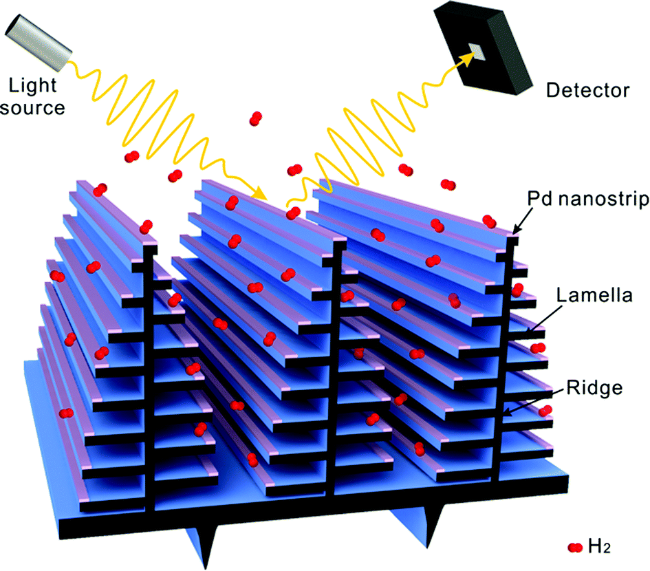 | ||
| Fig. 1 Schematic illustration showing optical H2 sensing based on the 3D heterogeneous structures that are consisted of Pd nanostrips and the photonic architectures of the Morpho butterfly wing scales. | ||
The Morpho sulkowskyi butterfly was chosen as model for the fabrication of H2 sensing platform. As shown in Fig. 2a, the Morpho butterfly wing displays brilliant blue iridescence originated from the elaborate hierarchical photonic structures of the scales. The scales are regularly arranged on the wing surface, as presented in Fig. 2b. They are ∼200 μm in length and ∼50 μm in width (Fig. 2c). On each scale, there are ordered arrays of ridges running along the longitudinal direction and adjacent ridges are connected each other by cross-ribs in the transversal direction, as presented in Fig. 2d. The high magnification scanning electron microscopy (SEM) image in the inset of Fig. 2d shows that the ridges contain multilayered lamellae folds. The details of the multilayered structures are shown by a cross-section transmission electron microscopy (TEM) image of ridges in Fig. 2e, which reveals the Christmas tree-like structures. A stem with width of 50–120 nm stands at the middle of each ridge. Approximately eight lamellae that are separated by air decorate at both sides of the stem, with the width of lamella gradually decreasing from the bottom to the top of the stem. The average thicknesses of lamella and the spacing between the lamella are ∼65 nm and ∼150 nm, respectively. Multilayer interference of light from the lamella layers, in combination with the light diffraction from the arrays of the ridges, contributes to the iridescence color appearance of the butterfly wing.42,43 We used the PVD method to deposit Pd coating on the butterfly wing structures. Considering the formation of the continuous coating and the response time of the 3D structure, we set the thickness of the Pd coating at 15 nm. During the deposition of Pd, the butterfly wing was placed directly under a Pd source so that the Pd coating was deposited vertically onto the butterfly wing structures. After coating the Pd layer, the edge portions of the lamellae were covered with Pd, resulted in selective modification of photonic structures of butterfly wing scales with Pd nanostrips, as shown in Fig. 2f and S1.†
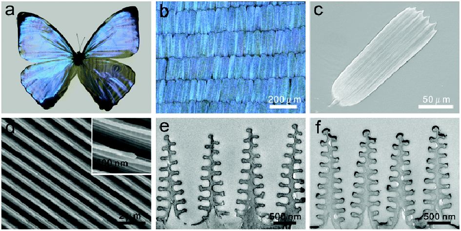 | ||
| Fig. 2 Morphologies and structures of the Morpho butterfly wing before and after selective modification with Pd. (a) The photo of the Morpho sulkowskyi butterfly. (b) Optical microscopy image of the stacked scales on the wing surface. (c) SEM image of a single butterfly wing scale supported on a silicon substrate. (d) Top SEM view of the photonic architecture of the scale. The inset figure is a high magnification SEM showing the multilayered lamella structures. (e) TEM image of a transverse section of the scale showing ridges with lamella structures. (f) TEM image showing the selectively modified ridges, where the edge of each lamella was coated with Pd nanostrip. | ||
We investigated the optical reflectance of the Pd-modified butterfly wing at normal incidence. Compared with the reflectance spectra of original scales, the reflectance of Pd-modified butterfly wing scales with a Pd layer of about 15 nm in thickness exhibited a main peak, which underwent blue shift from ∼485 nm to ∼460 nm and also showed smaller full width at half maximum than the original scales, as shown in Fig. 3a and b. Moreover, decorating of the Morpho scales with Pd nanostrips produced a decrease in the reflectance along with a minor peak at the wavelength near the violet end of the reflection spectra as well as a weak peak at ∼560 nm. These spectral changes were most likely due to the interaction of the reflection band originated from butterfly wing structures with the plasmonic absorption from the Pd nanostrips on the wing structures. In order to study this optical interaction, the reflectance spectra for the original butterfly structures and the butterfly structures decorated with Pd nanostrips were calculated through finite-difference time-domain (FDTD) methods, as presented in Fig. 3c and d, respectively. The simulated reflectance spectra exhibited good matching with the corresponding experimental results. We also performed simulations to separately analyze the plasmonic absorption of Pd nanostrips, as shown in Fig. S2.† The calculated absorption cross-section revealed the broad plasmonic absorption band of Pd nanostrip, which overlaps with the reflection band of butterfly wing structures. Besides, we computed the electric-field distributions of the Pd nanostrips on a planar dielectric substrate (Fig. S3†) and the butterfly wing structures with Pd nanostrips (Fig. 3e) at resonance, respectively. The light was concentrated at the tips of the Pd nanostrips and larger enhancement was observed in the case of the Pd nanostrips distributed in the butterfly wing structures, which indicated that the interaction of light with Pd nanostrips were enhanced by coupling to the optical cavity of Morpho butterfly scales. As such, the plasmonic mode of Pd nanostructures could effectively interplay with resonant mode of the biophotonic nanostructures, which thus was expected to enhance the sensitivity in H2 sensing.
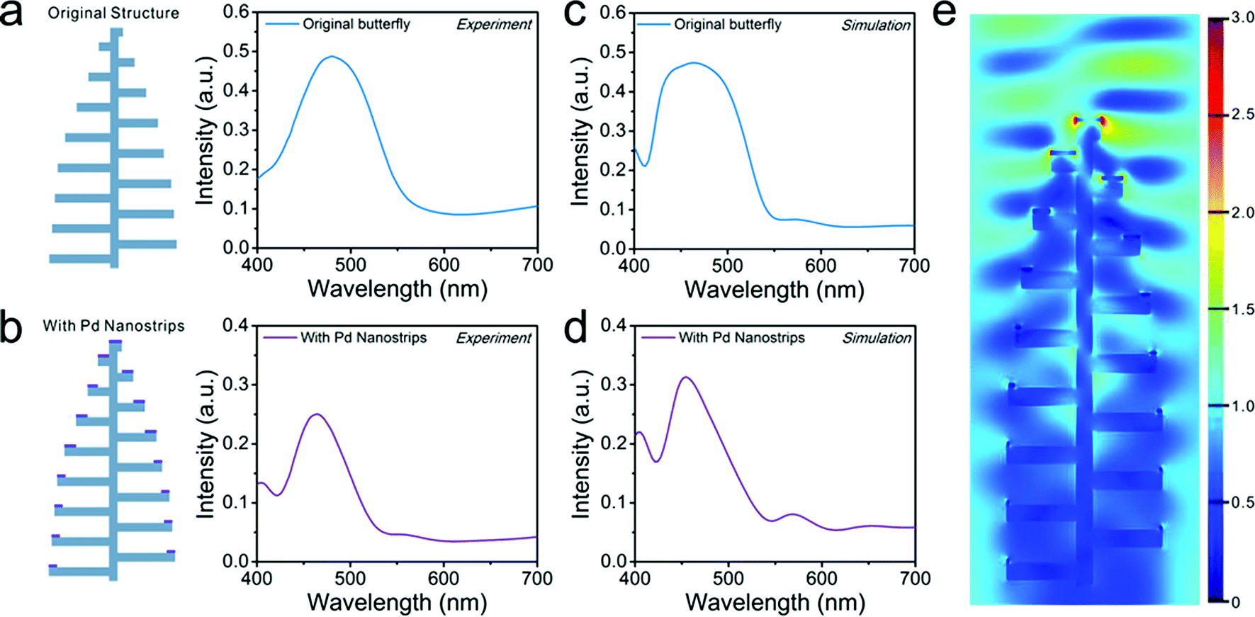 | ||
| Fig. 3 Optical properties of the original butterfly wing scales and the modified scales with Pd nanostrips. (a) Measured reflectance spectra of the original Morpho butterfly wing. (b) Measured reflectance spectra of the modified butterfly wing scales with Pd nanostrips. (c) Calculated reflectance spectra of the original Morpho butterfly scales. (d) Calculated reflectance spectra of Pd-modified butterfly scales. (e) The simulated electric field distribution at the wavelength of 500 nm showing the enhanced light–matter interaction in the Pd nanostrips distributed in the butterfly wing structures. | ||
To examine the response of Pd-modified butterfly wing scales to the exposure of H2, the butterfly wing sample was placed in a glass chamber with an optical fiber mounted through the top hatch at room temperature, as shown in Fig. S4.† The chamber was connected to a gas inlet channel for H2 and nitrogen (N2) carrier gas that were premixed before flowing into the chamber. The concentration of H2 was regulated through changing the gas flow of N2 and H2 with two mass flow controllers. We recorded the reflectance spectra of the sample at different H2 concentrations. To evaluate the changes in reflectance spectra following H2 exposures, we calculated the relative reflectance ΔR(λ) according to44
| ΔR(λ) = 100% × [R(λ)/R0(λ)] | (1) |
Fig. 4a showed relative reflectance of the Pd-modified butterfly wing scales with respect to different H2 concentrations over a range from 0.001% to 4%. Exposure to H2 caused the reflectance increase, and the pronounced ΔR response was over the wavelength region of 400–550 nm, which took place in the same wavelength range of the strong interaction between the plasmonic mode of Pd nanostructures and resonant mode of the biophotonic nanostructures. The reflectance of the original Morpho butterfly wing scales with respect to different H2 concentrations over a range from 0.1% to 4% also was measured, which suggested that there was no obvious response (Fig. S5†). In the presence of H2, the Pd nanostrips dissociated H2 molecules and absorbed the H atoms to form Pd hydride, typically accompanied by lattice expansion and the change of dielectric properties to less metallic. As a result, the plasmonic absorption of the Pd nanostrip was altered and the spectral variations of the heterogeneous structures were induced. The increase in the reflectance response of the Pd-modified butterfly wing was observed with the increase in H2 concentration, which was attributed to the larger change of dielectric function and volume expansion.
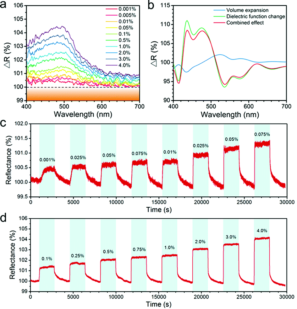 | ||
| Fig. 4 Response of the Pd-modified photonic architectures to H2 gas. (a) Relative reflectance measured in different H2 concentrations. (b) The simulated relative reflectance of the Pd-modified butterfly scales due to expansion and change in dielectric function when Pd is converted into β-PdHx. (c) Normalized reflectance change at wavelength of 500 nm in different H2 concentrations showing a detection limit below 10 ppm. (d) Normalized reflectance change at wavelength of 500 nm in different H2 concentrations from 0.1% to 4%. | ||
To further understand the sensing mechanism, we carried out simulations to compare the reflectance of Pd-modified butterfly scales as well as the Pd nanostrips on a planar dielectric substrate before and after H2 uptake, as shown in Fig. 4b and S6.† For simplicity, we assumed that the Pd was completely converted into β-phase (β-PdHx) after the exposure of H2 gas. In the simulations, we examined the contributions of two factors: volume expansion and the change in dielectric function. The volume expansion of Pd nanostrips alone led to a little decrease in the ΔR(λ) spectra of the heterogeneous structures over the short-wavelength range and slight increase over the long-wavelength range. The change in dielectric function led to a clear increase in the ΔR(λ) spectra over the 430–510 nm. The calculated results of the combined effects of volume expansion and the change in dielectric function suggested that the change of dielectric function has more influence on the optical response of the Pd-modified biophotonic structures. The calculated ΔR(λ) spectra in Fig. 4b are in general agreement with the experimental spectra (Fig. 4a). The pronounced feature in calculated and experimental spectra was the increase in the ΔR(λ) spectra over the wavelength range of the strong interaction between the plasmonic mode and the resonant mode of the biophotonic nanostructures.
The dynamic change of reflectance for the Pd-modified butterfly wing sample at the wavelength of 500 nm were shown in Fig. 4c and d. The optical response clearly showed the dependence on the H2 concentration. For comparison, the temporal reflectance was normalized to the reflectance of the sample in pure N2. As the concentration of H2 increased, the normalized reflectance at wavelength of 500 nm increased, and the sensor exhibited a lowest detectable response at concentrations of 10 ppm. The low noise level relative to the response indicated a detection limit less than 10 ppm, which is among the lowest detection limit for optical H2 sensing based on plasmonic Pd nanostructures.13,19,30 The high sensitivity of the Pd-modified butterfly wing scales mainly arose from the synergetic effect between Pd nanostrips and biophotonic structures.
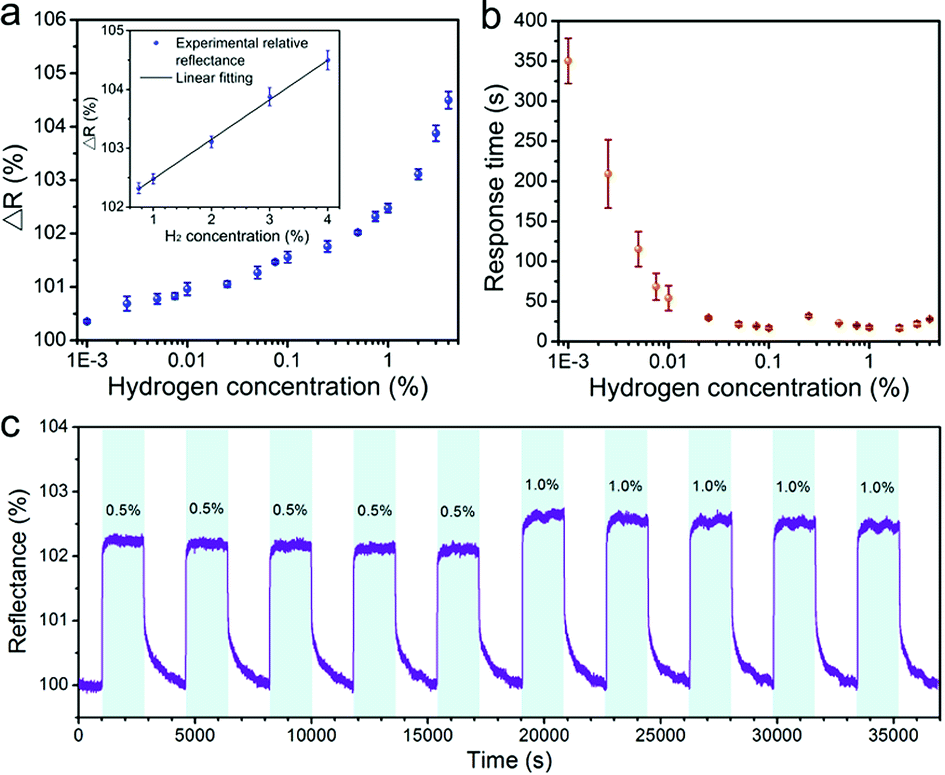
Furthermore, the reflectance change at the wavelength of 500 nm as a function of H2 concentration in the range from 0.001% to 4% suggested a positive relationship (Fig. 5a). It is worth to note that a linear relationship between the reflectance change and the H2 concentrations was observed within the high concentration range from 0.75% to 4% (inset of Fig. 5a), which is approximately corresponding to the regimes of mixed α + β-phase and the β-phase Pd hydride.4,30 We also measured the response time of the Pd-modified butterfly wing scales at different H2 concentrations (Fig. 5b). The response time was defined as the time needed to reach 90% of the equilibrium ΔR. As depicted in Fig. 5b, when H2 concentration increased, the response time decreased first, and then gradually became relatively stable. The observed response time is within the range of response time reported so far.27,33 The sensing speed could be further improved by using different materials such as the Pd alloys.45
 | ||
| Fig. 5 Sensing performance of the Pd-modified Morpho butterfly scales to H2. (a) The plot showing relative reflectance at wavelength of 500 nm for different H2 concentrations. The inset figure shows a good linear relation between the relative reflectance and the H2 concentration at the range of 0.75–4%. (b) The response time for different H2 concentrations. (c) Five cycles of H2 exposure for concentrations of 0.5% and 1%. | ||
In addition, we monitored the optical response of our sensor during five on/off H2 cycles at the concentration of 0.5% and 1%, respectively. The temporal response of normalized reflectance at the wavelength of 500 nm was shown in Fig. 5c. The Pd-modified butterfly wing scales exhibited a rather consistent response for each repeated cycle, which suggested a good repeatability and stability of H2 sensing.
For investigation of the selective response of the Pd-modified Morpho butterfly wing scales, the relative reflectances upon exposure to H2 and several potential interfering gases, including O2, CO2, and CH4 were compared, as shown in Fig. S7.† The responses from the interfering gases were much less than that observed for H2 at similar concentration, indicating that the 3D heterogeneous structure has a little cross-sensitivity to these interfering gases.
Conclusions
In summary, we presented a bioinspired 3D heterogeneous structure that was achieved by selectively modification of Morpho butterfly wing scales with Pd for sensitive H2 sensing at room temperature. The plasmonic mode in Pd nanostrips was effectively coupled with the optical resonant mode of the biophotonic nanostructures in the as-fabricated Pd-modified butterfly wing scales, which produced a sharp major peak in reflectance spectra and yielded an enhancement of light interaction with Pd nanostrips. Both the experiments and simulations demonstrated that the pronounced response of the reflectance spectra to the exposure of H2 was occurred over the wavelength range of the strong interplay between the plasmonic mode and the optical resonant mode. Due to the synergetic effect of Pd nanostrips and biophotonic structures, the Pd-modified butterfly scales exhibited high sensitivity to H2 with a detection limit below 10 ppm. Besides, the fabricated optical H2 sensor also showed fast response and good repeatability. The bioinspired H2 sensing system, which is based on the combination of plasmonic nanostructures with photonic crystal structures, not only provides a promising approach for high-performance optical H2 sensor, but also offers a strategy of developing future nanoengineered structures for various sensing applications.Conflicts of interest
There are no conflicts to declare.Acknowledgements
We are grateful to the financial support from National Key R&D Program of China (2016YFB0402100), National Natural Science Foundation of China (Grant No: 51521004, 51420105009, 51403127, 21401129), the 111 Project (Grant No: B16032) and “Chen Guang” project from Shanghai Municipal Education Commission. Thanks Ge Wang and Yanhua Zhu from the Instrumental Analysis Center of Shanghai Jiao Tong University for help with the TEM samples.References
- G. Cipriani, V. Di Dio, F. Genduso, D. La Cascia, R. Liga, R. Miceli and G. Ricco Galluzzo, Int. J. Hydrogen Energy, 2014, 39, 8482–8494 CrossRef.
- S. Singh, S. Jain, V. Ps, A. K. Tiwari, M. R. Nouni, J. K. Pandey and S. Goel, Renewable Sustainable Energy Rev., 2015, 51, 623–633 CrossRef.
- T. Hübert, L. Boon-Brett, G. Black and U. Banach, Sens. Actuators, B, 2011, 157, 329–352 CrossRef.
- F. D. Manchester, A. San-Martin and J. M. Pitre, J. Phase Equilib., 1994, 15, 62–83 CrossRef.
- M. E. Nasir, W. Dickson, G. A. Wurtz, W. P. Wardley and A. V. Zayats, Adv. Mater., 2014, 26, 3532–3537 CrossRef PubMed.
- F. Favier, E. C. Walter, M. P. Zach, T. Benter and R. M. Penner, Science, 2001, 293, 2227–2231 CrossRef PubMed.
- Y. T. Pan, X. Yin, K. S. Kwok and H. Yang, Nano Lett., 2014, 14, 5953–5959 CrossRef PubMed.
- X. Li, M. Le Thai, R. K. Dutta, S. Qiao, G. T. Chandran and R. M. Penner, ACS Sens., 2017, 2, 282–289 CrossRef PubMed.
- M. Chen, P. Mao, Y. Qin, J. Wang, B. Xie, X. Wang, D. Han, G. H. Wang, F. Song, M. Han, J. M. Liu and G. Wang, ACS Appl. Mater. Interfaces, 2017, 9, 27193–27201 CrossRef PubMed.
- Z. Zhao, Y. Sevryugina, M. A. Carpenter, D. Welch and H. Xia, Anal. Chem., 2004, 76, 6321–6326 CrossRef PubMed.
- Y.-n. Zhang, H. Peng, X. Qian, Y. Zhang, G. An and Y. Zhao, Sens. Actuators, B, 2017, 244, 393–416 CrossRef.
- Y. Shen, X. She and C. Jin, ACS Photonics, 2018, 5, 1334–1342 CrossRef.
- I. Zoric, E. M. Larsson, B. Kasemo and C. Langhammer, Adv. Mater., 2010, 22, 4628–4633 CrossRef PubMed.
- T. Shegai, P. Johansson, C. Langhammer and M. Kall, Nano Lett., 2012, 12, 2464–2469 CrossRef PubMed.
- M. A. Poyli, V. M. Silkin, I. P. Chernov, P. M. Echenique, R. D. Muino and J. Aizpurua, J. Phys. Chem. Lett., 2012, 3, 2556–2561 CrossRef PubMed.
- C. Wadell, S. Syrenova and C. Langhammer, ACS Nano, 2014, 8, 11925–11940 CrossRef PubMed.
- K. Ikeda, S. Uchiyama, M. Takase and K. Murakoshi, ACS Photonics, 2015, 2, 66–72 CrossRef.
- F. A. Nugroho, B. Iandolo, J. B. Wagner and C. Langhammer, ACS Nano, 2016, 10, 2871–2879 CrossRef PubMed.
- K. C. Ng, F.-C. Lin, P.-W. Yang, Y.-C. Chuang, C.-K. Chang, A.-H. Yeh, C.-S. Kuo, C.-R. Kao, C.-C. Liu, U. S. Jeng, J.-S. Huang and C.-H. Kuo, Chem. Mater., 2017, 30, 204–213 CrossRef.
- M. Matuschek, D. P. Singh, H. H. Jeong, M. Nesterov, T. Weiss, P. Fischer, F. Neubrech and N. Liu, Small, 2018, 14, 1702990 CrossRef PubMed.
- C. Langhammer, Z. Yuan, I. Zoric and B. Kasemo, Nano Lett., 2006, 6, 833–838 CrossRef PubMed.
- C. Langhammer, I. Zoric, B. Kasemo and B. M. Clemens, Nano Lett., 2007, 7, 3122–3127 CrossRef PubMed.
- C. Langhammer, V. P. Zhdanov, I. Zoric and B. Kasemo, Phys. Rev. Lett., 2010, 104, 135502 CrossRef PubMed.
- F. Yang, S. C. Kung, M. Cheng, J. C. Hemminger and R. M. Penner, ACS Nano, 2010, 4, 5233–5244 CrossRef PubMed.
- J. M. Sanz, D. Ortiz, R. Alcaraz de la Osa, J. M. Saiz, F. González, A. S. Brown, M. Losurdo, H. O. Everitt and F. Moreno, J. Phys. Chem. C, 2013, 117, 19606–19615 CrossRef.
- T. Pakizeh, C. Langhammer, I. Zoric, P. Apell and M. Kall, Nano Lett., 2009, 9, 882–886 CrossRef PubMed.
- A. Tittl, P. Mai, R. Taubert, D. Dregely, N. Liu and H. Giessen, Nano Lett., 2011, 11, 4366–4369 CrossRef PubMed.
- T. Shegai and C. Langhammer, Adv. Mater., 2011, 23, 4409–4414 CrossRef PubMed.
- C. Langhammer, E. M. Larsson, B. Kasemo and I. Zoric, Nano Lett., 2010, 10, 3529–3538 CrossRef PubMed.
- A. Yang, M. D. Huntington, M. F. Cardinal, S. S. Masango, R. P. Van Duyne and T. W. Odom, ACS Nano, 2014, 8, 7639–7647 CrossRef PubMed.
- N. Liu, M. L. Tang, M. Hentschel, H. Giessen and A. P. Alivisatos, Nat. Mater., 2011, 10, 631–636 CrossRef PubMed.
- C. Wadell and C. Langhammer, Nanoscale, 2015, 7, 10963–10969 RSC.
- C. Y. Chiu and M. H. Huang, Angew. Chem., Int. Ed., 2013, 52, 12709–12713 CrossRef PubMed.
- R. Jiang, F. Qin, Q. Ruan, J. Wang and C. Jin, Adv. Funct. Mater., 2014, 24, 7328–7337 CrossRef.
- H. K. Yip, X. Zhu, X. Zhuo, R. Jiang, Z. Yang and J. Wang, Adv. Opt. Mater., 2017, 5, 1700740 CrossRef.
- S. Rodal-Cedeira, V. Montes-García, L. Polavarapu, D. M. Solís, H. Heidari, A. La Porta, M. Angiola, A. Martucci, J. M. Taboada, F. Obelleiro, S. Bals, J. Pérez-Juste and I. Pastoriza-Santos, Chem. Mater., 2016, 28, 9169–9180 CrossRef.
- M. L. Tang, N. Liu, J. A. Dionne and A. P. Alivisatos, J. Am. Chem. Soc., 2011, 133, 13220–13223 CrossRef PubMed.
- X. Yang, Z. Peng, H. Zuo, T. Shi and G. Liao, Sens. Actuators, A, 2011, 167, 367–373 CrossRef.
- R. A. Potyrailo, T. A. Starkey, P. Vukusic, H. Ghiradella, M. Vasudev, T. Bunning, R. R. Naik, Z. Tang, M. Larsen, T. Deng, S. Zhong, M. Palacios, J. C. Grande, G. Zorn, G. Goddard and S. Zalubovsky, Proc. Natl. Acad. Sci. U. S. A., 2013, 110, 15567–15572 CrossRef PubMed.
- F. Zhang, Q. Shen, X. Shi, S. Li, W. Wang, Z. Luo, G. He, P. Zhang, P. Tao, C. Song, W. Zhang, D. Zhang, T. Deng and W. Shang, Adv. Mater., 2015, 27, 1077–1082 CrossRef PubMed.
- D. Xu, H. Yu, Q. Xu, G. Xu and K. Wang, ACS Appl. Mater. Interfaces, 2015, 7, 8750–8756 CrossRef PubMed.
- A. D. Pris, Y. Utturkar, C. Surman, W. G. Morris, A. Vert, S. Zalyubovskiy, T. Deng, H. T. Ghiradella and R. A. Potyrailo, Nat. Photonics, 2012, 6, 195–200 CrossRef.
- P. Vukusic, J. R. Sambles, C. R. Lawrence and R. J. Wootton, Proc. R. Soc. London, Ser. B, 1999, 266, 1403–1411 CrossRef.
- R. A. Potyrailo, H. Ghiradella, A. Vertiatchikh, K. Dovidenko, J. R. Cournoyer and E. Olson, Nat. Photonics, 2007, 1, 123–128 CrossRef.
- C. Wadell, F. A. Nugroho, E. Lidstrom, B. Iandolo, J. B. Wagner and C. Langhammer, Nano Lett., 2015, 15, 3563–3570 CrossRef PubMed.
Footnote |
| † Electronic supplementary information (ESI) available. See DOI: 10.1039/c8ra05046e |
| This journal is © The Royal Society of Chemistry 2018 |