
 Open Access Article
 This Open Access Article is licensed under a Creative Commons Attribution-Non Commercial 3.0 Unported Licence
Pure exciplex-based white organic light-emitting diodes with imitation daylight emissions†
Dian Luoa,
Chung-Tsung Hsieha,
Yen-Po Wanga,
Thomas C. Chuangb,
Hsin-Hua Changc and
Chih-Hao Chang *a
*a
aDepartment of Electrical Engineering, Yuan Ze University, Chung-Li, Taiwan 32003. E-mail: chc@saturn.yzu.edu.tw; Fax: +886 34638800 ext. 7517; Tel: +886 34514281
bDepartment of Information Science and Technology, Vanung University, Chung-Li, Taiwan 32061
cDepartment of Aeronautical and Opto-Mechatronic Engineering, Vanung University, Chung-Li, Taiwan 32061
First published on 30th August 2018
Abstract
An exciplex could be formed by blending a selected hole-transporting material (HTM)/electron-transporting material (ETM) pair, and the corresponding energy band gap is roughly determined by the energy difference between the lowest unoccupied molecular orbital (LUMO) of the ETM and the highest occupied molecular orbital (HOMO) of the HTM. In this study, three HTM/ETM combinations are adopted to generate blue, green, and red exciplexes, allowing us to design precise device architectures for the fabrication of exciplex-based white OLEDs (WOLEDs) with daylight-like emissions. The CIE coordinates of this WOLED varied close to the Planckian locus as the biases increase, with a high color rendering index of about 96. This high performance suggests this exciplex-based WOLED can provide high-quality white-light illumination. Photoluminance and lifetime measurements of the exciplex behavior of the HTM/ETM combinations indicate that the HTM and ETM selected should possess higher triplet energy bandgaps than those of their corresponding exciplex to avoid energy loss.
Introduction
The properties of organic light-emitting diodes (OLEDs) have received considerable attention, including their high contrast ratio, fast response time, high efficiency, etc. OLED development has gradually shifted from fluorescence to phosphorescence because phosphorescent materials can potentially harvest both singlet and triplet excited states to render an ideal internal quantum efficiency of 100%. Although phosphorescent OLEDs can potentially meet the requirements of practical display and lighting applications, phosphorescent emitters consisting of precious metals are expensive to produce. In addition, the device lifetimes of blue phosphorescent OLEDs still leave something to be desired because a phosphorescent guest and its corresponding host materials with wide energy bandgaps still suffer from insufficient electrochemical and thermal stability. Therefore, blue OLEDs still primarily rely on fluorescent materials which have an upper limit efficiency of only 25%. Recently, efficient OLEDs have been developed through two alternative techniques including exciplex and thermally-activated delayed fluorescence (TADF). A TADF material requires a small energy band gap between the first triplet excited state and the first singlet excited state (ΔEST), allowing for the collection of triplet excitons via reverse intersystem crossing.1–3 Similarly, a small ΔEST can be achieved with an exciplex generated by through-space intermolecular charge transfer between a hole-transporting material (HTM) and an electron-transporting material (ETM).4–6The exciplex could be easily formed by applying commercially available materials.10,11 Exciplex-based OLEDs can also be very efficient given appropriate HTM and ETM in the emitting layer (EML). In general, an exciplex could be generated using a bilayer structure with both HTM and ETM or by directly mixing an HTM and an ETM. The latter typically results in greater exciplex production yields. In principle, since the exciplex energy band gap is determined by the energy-level difference, the energy band gap could be adjusted by choosing appropriate materials. For instance, the energy band gap could be determined by the energy difference between the lowest unoccupied molecular orbital (LUMO) of the ETM and the highest occupied molecular orbital (HOMO) of the HTM.7–13
OLEDs which can effectively imitate daylight would be of particular use in high-latitude areas where sunlight exposure is highly seasonal.14–16 In 2009, Jou et al. proposed a sunlight-style OLED with a correlated color temperature (CCT) tunable from 2300 to 12![[thin space (1/6-em)]](https://www.rsc.org/images/entities/char_2009.gif) 000 K, proving the possibility of fabricating a new low color temperature light source.17 In 2013, the same group reported OLEDs with a candle light-style yellowish orange chromaticity with a power efficiency of 29 lm W−1 at 100 cd m−2, a respective color rendering index (CRI) of 87 and a CCT of 2050 K.18 The fabricated device minimized potential harmful effects of excessive blue emission on the human eye. In 2014, they demonstrated the feasibility of creating indoor sunset hues using a dusk-light-style OLED that exhibits a CCT ranging between 1500 and 3000 K.19 The artificial dusk hue shows a 92 color rendering index at 2745 K with an 87% luminance spectrum resemblance with the sunset hue. However, all these devices used the host–guest system in the EML, which not only requires expensive molecular emitters but also suffers from different rates of degradation of the emitters. Herein, we propose a pure exciplex-based white OLED (WOLED) with a delicate device architecture design which can generate emissions that approximate daylight, where the WOLED emission color closely tracks the Planckian locus.20,21
000 K, proving the possibility of fabricating a new low color temperature light source.17 In 2013, the same group reported OLEDs with a candle light-style yellowish orange chromaticity with a power efficiency of 29 lm W−1 at 100 cd m−2, a respective color rendering index (CRI) of 87 and a CCT of 2050 K.18 The fabricated device minimized potential harmful effects of excessive blue emission on the human eye. In 2014, they demonstrated the feasibility of creating indoor sunset hues using a dusk-light-style OLED that exhibits a CCT ranging between 1500 and 3000 K.19 The artificial dusk hue shows a 92 color rendering index at 2745 K with an 87% luminance spectrum resemblance with the sunset hue. However, all these devices used the host–guest system in the EML, which not only requires expensive molecular emitters but also suffers from different rates of degradation of the emitters. Herein, we propose a pure exciplex-based white OLED (WOLED) with a delicate device architecture design which can generate emissions that approximate daylight, where the WOLED emission color closely tracks the Planckian locus.20,21
Experimental
OLED fabrication and characterization
The multilayer OLED devices were fabricated on glass substrates which had the typical structure with the organic layers sandwiched between a bottom ITO (120 nm) anode and a top metal cathode. After routine ultra-sonication cleaning of the indium tin oxide (ITO) coated glass in deionized water and organic solvents, the ITO-coated glass was pre-treated with UV–ozone for 5 minutes. The organic and metal layers were deposited onto ITO substrate by thermal evaporation in a vacuum chamber with a base pressure of about 10−6 torr. Device fabrication was completed in a single cycle without breaking the vacuum. The active area was defined by a shadow mask (2 × 2 mm2). Current density–voltage–luminance (J–V–L) characterization was measured using a Keithley 238 current source-measure unit and a Keithley 6485 pico-ammeter equipped with a calibrated Si-photodiode. The electroluminescent spectra were recorded using an Ocean Optics spectrometer.Photophysical measurements
Thin films for photophysical characterization were prepared by thermal evaporation on quartz substrates in a vacuum chamber. The fluorescence spectra, phosphorescence spectra, and lifetime measurements were characterized by using a fluorescence spectroscopy (HORIBA-fluoromax plus). Phosphorescence spectra of thin films or dilute solution (toluene) were conducted at 77 K by the spectrometer equipped with a microsecond flash Xe lamp as the pulsed excitation source. Different delay timescales were inserted between the pulsed excitation to collect the emission spectra. Time-resolved PL (TRPL) was measured by monitoring the decay of the intensity at the PL peak wavelength using the time-correlated single-photon counting technique with a nanosecond pulsed light-emitting diode (320 nm).Results and discussion
Device architecture designs for exciplex-based OLEDs
To demonstrate our idea, all selected materials for the tested devices used commercially available compounds. Two commonly used HTMs, 4,4′,4′′-tris(N-3-methylphenyl-N-phenyl-amino)triphenylamine (m-MTDATA)22 and 4,4′,4′′-tris(carbazol-9-yl)-triphenylamine (TCTA),23 were respectively selected as hole transport layer or the HTM for the EMLs. In addition, 3,5,3′,5′-tetra(m-pyrid-3-yl)-phenyl[1,1′]biphenyl (BP4mPy),24 1,3,5-tris[(3-pyridyl)phen-3-yl]benzene (TmPyPB),25 and 4,6-bis(3,5-di(pyridin-3-yl)phenyl)-2-methylpyrimidine (B3PyMPM)26 are used as the electron transport layer or the ETM in the EMLs. Three combinations of HTM and ETM were used to produce an exciplex which was responsible for the blue to red emission shift. Since the energy band gap of exciplex is determined by the energy difference between the LUMO of the ETM and the HOMO of the HTM. Therefore, the emission color of the exciplex could be roughly estimated according to their energy levels before device fabrication. According to previous literature, the LUMO of BP4mPy, TmPyPB, and B3PyMPM were estimated to be around 2.57 eV, 2.73 eV, and 3.20 eV, respectively.24–26 In addition, the respective HOMO of TCTA and m-MTDATA were estimated to be around 5.80 eV and 5.10 eV.22,23 Thus, the respective LUMO/HOMO differences for the following combinations are: 4.09 eV for TCTA:BP4mPy, 2.37 eV for m-MTDATA:TmPyPB, and 1.90 eV for m-MTDATA:B3PyMPM. They then could generate blue, green, and red emissions, respectively.
On the other hand, to imitate daylight emissions, the main carrier recombination zone was set at the red EML, producing an intense red emission at lower biases. In addition, a proper device architecture design will allow the carrier recombination zone to progressively extend to the green and blue EMLs as the forward bias increases. Hence, one could expect that the emission color of OLEDs might vary from red to white. Furthermore, a wide energy bandgap material, 2,6-bis(3-(9H-carbazol-9-yl)phenyl)pyridine (26DCzppy),27 with bipolar transport capability was inserted between the green and red EMLs to ensure the recombination zone formed at the red EML at a lower bias. This buffer layer could help adjust the carrier transport and the exciton diffusion.28
Two kinds of exciplex-based WOLEDs are examined. Device A with double EMLs is configured as ITO (120 nm)/TCTA (40 nm)/TCTA 50 wt%:BP4mPy 50 wt% (29 nm)/26DCzPPy (3 nm)/m-MTDATA 10 wt%:B3PyMPM 90 wt% (3 nm)/TmPyPB (50 nm)/LiF (0.8 nm)/Al (150 nm), for which LiF and aluminum are respectively used as the electron injection layer and reflective cathode. The first EML consisting of TCTA 50 wt%:BP4mPy 50 wt% is responsible for the blue emission, while the second EML for the red light was set as m-MTDATA 10 wt%:B3PyMPM 90 wt%. Moreover, the mixing ratio of the aforementioned exciplex-based EMLs were fine-tuned to generate an appropriate white light emission. The device architecture of devices B1 and B2 with triple EMLs consisted of ITO (120 nm)/TCTA (40 nm)/TCTA 50 wt%:BP4mPy 50 wt% (29 nm)/m-MTDATA 80 wt%:TmPyPB 20 wt% (x nm)/26DCzPPy (3 nm)/m-MTDATA 10 wt%:B3PyMPM 90 wt% (3 nm)/TmPyPB (50 nm)/LiF (0.8 nm)/Al (150 nm). Compared to the architecture of device A, a green EML consisting of m-MTDATA 80 wt%:TmPyPB 20 wt% was inserted into the device next to the blue EMLs to improve the color rendering capability of the WOLEDs.29 The thicknesses of the green EMLs were varied to adjust the emission colors, e.g., 1 nm for device B1 and 3 nm for the second set of device B2. The corresponding chemical structures of the materials and the schematic structure of the device architectures are depicted in Fig. 1.
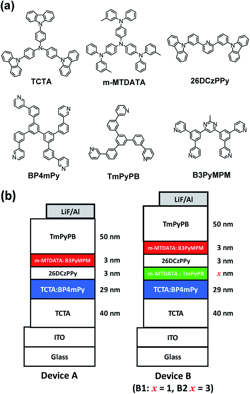 | ||
| Fig. 1 (a) Chemical structures of the materials; (b) the schematic structure of the device architectures. | ||
Fig. 2 shows the normalized EL spectra and the corresponding CIE coordinates of the tested exciplex-based OLEDs under different biases. From Fig. 2(a), device A exhibited a strong red emission at the lower biases and the blue emission peaks around 440 nm, which increased with the bias.30 However, the blue component was still much weaker than the red one even at higher voltages, resulting in device A's emission presenting a pinkish white color (cf. CIE coordinates shown in Fig. 2(d)). On the other hand, the EL spectra of both B1 and B2 showed three peaks with satisfactory emission color. The wavelengths of the deep-blue, sky-blue, and red emission peaks were respectively recorded at 385 nm, 462 nm, and 652 nm. Although devices B1 and B2 presented similarly intense red emissions at lower biases, and the emissions ranging from blue to green region gradually increased with voltage, the intensity of the emission ranging blue to green rose significantly at higher voltages, as shown in Fig. 2(b) and (c). Furthermore, the CIE coordinates of both devices B1 and B2 displayed pure white emission at higher biases. The varied emission of device B2 was close to the Planckian locus as the biases increased, indicating the sophisticated design of device B2. In addition, device B2 exhibited high CRI values of about 96 in a wide luminance range from 100 to 1000 cd m−2, corresponding to the CCT between 4359 and 7115 K. The numeric data collected from the EL spectra of device B2 are summarized in Table 1. We also included the corresponding data of devices A and B1 in Table S1 in ESI† for comparison. It's notable that the CRI value of device B2 reached the highest level compared to the previous reports.18 These performances demonstrate that this exciplex-based WOLED (i.e. B2) possessed a high-quality white-light illumination.28,31–35
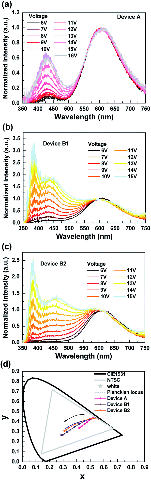 | ||
| Fig. 2 EL spectra of the tested exciplex-based white OLEDs with different operating voltages. (a) Device A; (b) device B1; (c) device B2; (d) CIE coordinates. | ||
| Voltage (V) | Luminance (cd m−2) | CIE coordinates (x, y) | CCT (K) | CRI |
|---|---|---|---|---|
| 6 | 1.76 | 0.533, 0.433 | 2071 | 70.20 |
| 7 | 5.41 | 0.497, 0.429 | 2364 | 75.66 |
| 8 | 15.13 | 0.456, 0.412 | 2762 | 81.05 |
| 9 | 36.37 | 0.421, 0.393 | 3201 | 85.77 |
| 10 | 79.99 | 0.388, 0.372 | 3744 | 89.71 |
| 11 | 168.75 | 0.363, 0.354 | 4359 | 92.80 |
| 12 | 302.37 | 0.341, 0.336 | 5162 | 95.06 |
| 13 | 493.91 | 0.323, 0.320 | 5998 | 96.07 |
| 14 | 720.35 | 0.309, 0.308 | 6972 | 96.05 |
| 15 | 914.58 | 0.306, 0.307 | 7115 | 95.69 |
Fig. 3 shows the schematic energy level diagram of the tested OLEDs. Given the large barrier at the B3PyMPM/26DCzPPy interface, the hole injection was smoother than the electron injection in device A. As indicated, the red component dominated the EL emission even as the voltage increased. In addition, abundant hole injection reinforced the carrier recombination occurring in m-MTDATA:B3PyMPM layer, increasing the possibility of exciton formation on m-MTDATA molecules. The blue emission peak around 430 nm should originate from m-MTDATA, which could be confirmed by the PL spectrum and will be discussed later (cf. Fig. 5(a)). Consequently, the original setting of blue EML (i.e. TCTA:BP4mPy) in device A was useless. In contrast, for the green EML inserted into devices B1 and B2, the hole would be partially trapped because of the low HOMO level of m-MTDATA, enabling appropriate adjustment of hole injection into the red EML. Thus, the electron could be transported to the green and blue EMLs and then recombine at higher voltages, creating much stronger green and blue emissions. Furthermore, by increasing the thickness of the green EML, the emission of device B2 could be adjusted to present a pure white color. As indicated, the corresponding CIE coordinates of device B2 vary along the Planckian locus as the biases increase.
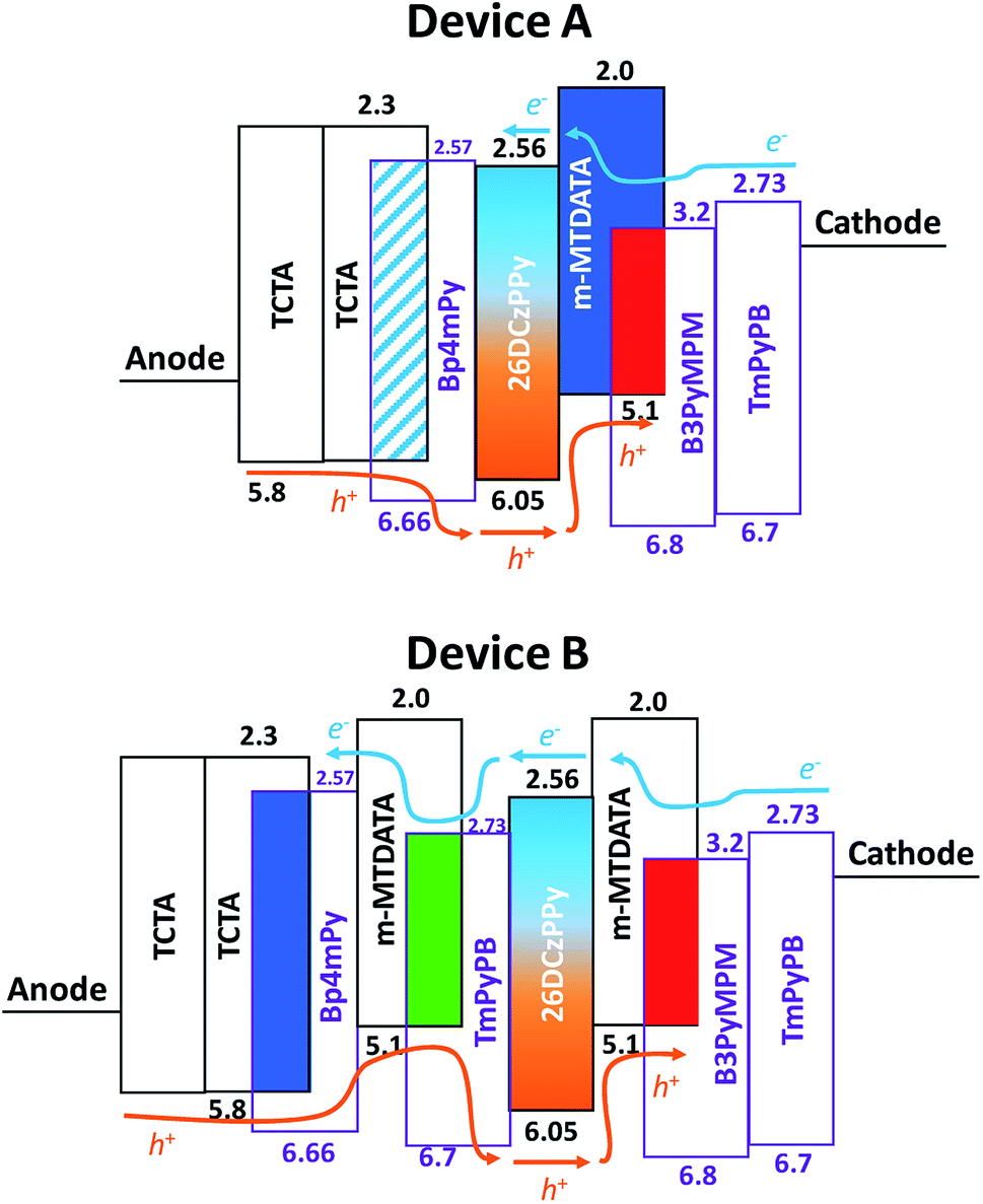 | ||
| Fig. 3 The schematic energy level diagram of devices A and B. | ||
Fig. 4 and S1† respectively depict the current density–voltage–luminance (J–V–L) curves and efficiency curves. From Fig. 4(a), as expected, devices B1 and B2 possesses additional green EML, showing lower current densities.36 In addition, the current density decreased as the thicknesses of the green EML increased. In contrast, the luminance of device B2 exhibited a higher maximum luminance than the other devices, due to human eye to green.37 The efficiency curves shown in Fig. 4(b) and S1† clearly indicate that a higher carrier balance could be obtained in device B2. The peak external quantum efficiency, luminance efficiency and power efficiency of device B2 were respectively 1.5%, 2.7 cd A−1, and 2.0 lm W−1. This WOLED efficiency was produced using commercially available materials to generate the exciplex. Although the efficiency was much lower than other state-of-art devices, this article focuses on the design of a feasible device architecture for exciplex-based WOLEDs to imitate daylight emissions. Moreover, device efficiency is expected to improve further by replacing the potential HTM/ETM combinations to achieving efficient increased efficiency as well the exciplex emissions.6,8,9,11,12,21
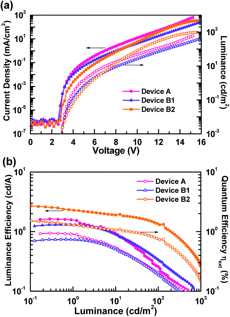 | ||
| Fig. 4 EL characteristics of the tested exciplex-based white OLEDs: (a) current density–voltage–luminance characteristics, (b) luminance efficiency vs. luminance of devices A, B1, and B2. | ||
Photophysical properties of the tested materials and the exciplex films
Fig. 5 shows the photoluminescence (PL) spectra and the corresponding excited-state lifetime measurements of the used materials. In addition, three thin-film samples composed of the used HTM/ETM mixture were also selected to examine the exciplex formation. The blending ratios of the three samples were the same as those used in the device. Samples B, G, and R respectively represent TCTA 50 wt%:BP4mPy 50 wt%, m-MTDATA 80 wt%:TmPyPB 20 wt%, m-MTDATA 10 wt%:B3PyMPM 90 wt%. Fig. 5(a) presents the PL spectra of the HTM and ETM measured in toluene at room temperature, while the PL spectra of samples A, B, and C are depicted in Fig. 5(b). Comparing Fig. 2(a) with Fig. 5(a), the emission peak around 430 nm shown in the EL spectra of device A should originate from m-MTDATA. As indicated, the PL spectra of the three samples were akin to the EL spectra of devices B1 and B2, confirming that the EL emission was the origin of the HTM/ETM mixtures. Furthermore, the emission peaks of all three samples were red-shifted as compared to the corresponding fluorescence of the used materials.38 Moreover, the respective full width at half maximum (FWFM) of the three samples were respectively estimated as 56, 106, and 142 nm. Evidently, the FWHM values of samples G and R were much wider than the fluorescence of the common organic emitters, which clearly demonstrated the exciplex formation.28,39,40 However, sample B did not present a typical exciplex emission with a broad spectral profile, but rather exhibited a narrower spectrum than those of samples G and R.
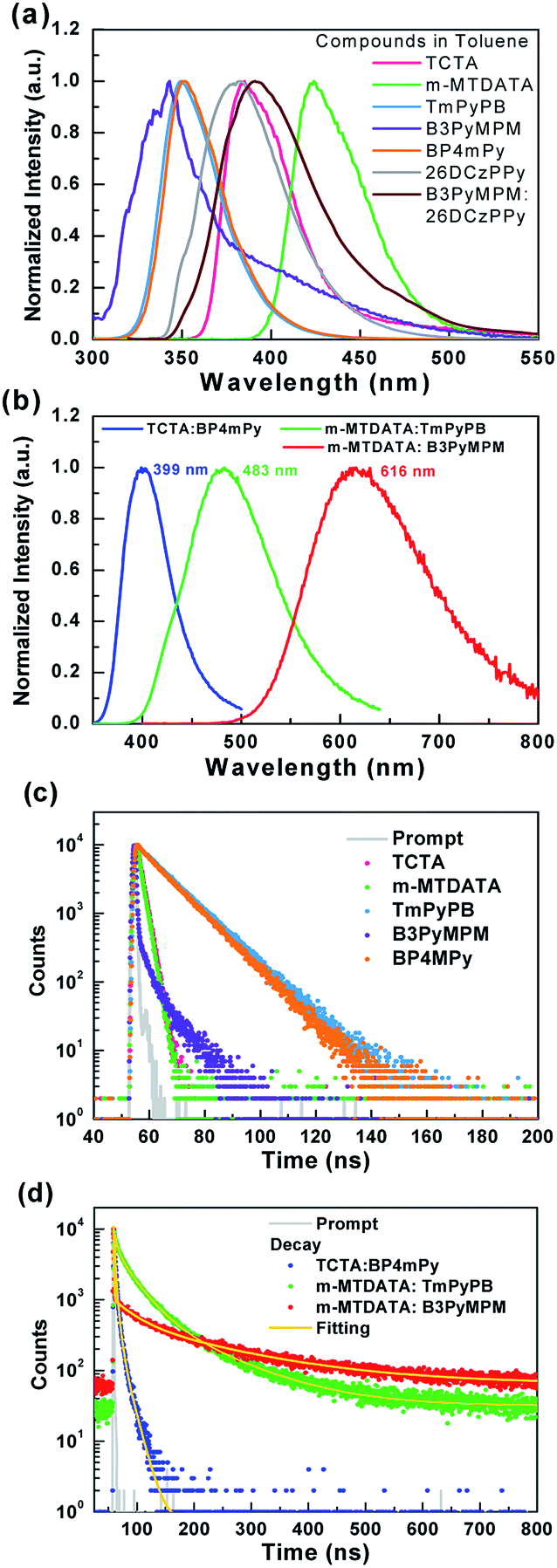 | ||
| Fig. 5 (a) PL spectra of the materials measured in toluene solution. (b) PL spectra of samples A, B, and C. (c) The decay characteristics of the materials in toluene solution. (d) The decay characteristics of samples A, B, and C. | ||
Fig. 5(c) shows the excited state decay characteristics of the materials in toluene solution. All materials exhibited typical fluorescent decay behavior. On the other hand, the curves exhibited in Fig. 5(d) clearly indicate that samples G and R possess two-component decay including a nanosecond-scale prompt and sub-microsecond-scale delayed components, while sample B had only a nanosecond-scale component. The delayed lifetimes for samples G and R were respectively estimated at 105.1 and 175.7 ns due to the slower reverse intersystem crossing processes from the T1 back to the S1 excited state.40 Moreover, the respective lifetime values of samples B, G, and R were estimated to be 5.3, 27.5, and 28.2 ns attributed to representative fluorescence decay.
From Fig. 5(b) and (d), sample B seems to exhibit the behavior typical of a fluorescent emitter. However, sample B shows a red-shifted spectrum compared to the fluorescence of TCTA and BP4mPy, suggesting that the emission origin of sample B is different from the S1 of TCTA or BP4mPy. Consequently, the phosphorescence of TCTA, BP4mPy, and sample B were measured in 77 K, as shown in Fig. 6(a). Both TCTA and BP4mPy possessed lower triplet energy bandgaps than that of sample B (i.e., TCTA:BP4mpy mixture). The triplet energy bandgaps of TCTA, BP4mPy, and sample B were evaluated based on the onset of the phosphorescent spectra and were respectively estimated to be 2.92, 2.94, and 3.31 eV. In addition, the phosphorescence of sample B was slightly red-shifted compared to the fluorescence. The small energy difference between the single and triplet excited states (ΔEST ∼0.1 eV) confirmed that the emission originated from the exciplex.7,9,39 Therefore, the related lower T1 states of TCTA and BP4mPy would offer pathways for exothermic energy transfer, leading to energy loss and thus a shorter lifetime for sample B. The photophysical properties of the used materials and the thin-film samples were summarized in Table 2. Furthermore, we measured the phosphorescence of sample B with different delay times, as shown in Fig. 6(b). The phosphorescence of exciplex gradually decayed with the extending delay time, while additional emissions appeared consisting of peaks similar to the BP4mPy's phosphorescence. These additional emissions could be seen as direct evidence of exothermic energy transfer. This was the first demonstration of the assumption indicating that the selected HTM and ETM should possess higher triplet energy bandgaps than those of their corresponding exciplex to avoid energy loss to the composed single molecules.41 Fig. 6(c) shows a schematic diagram of the energy transfers in samples B and R.
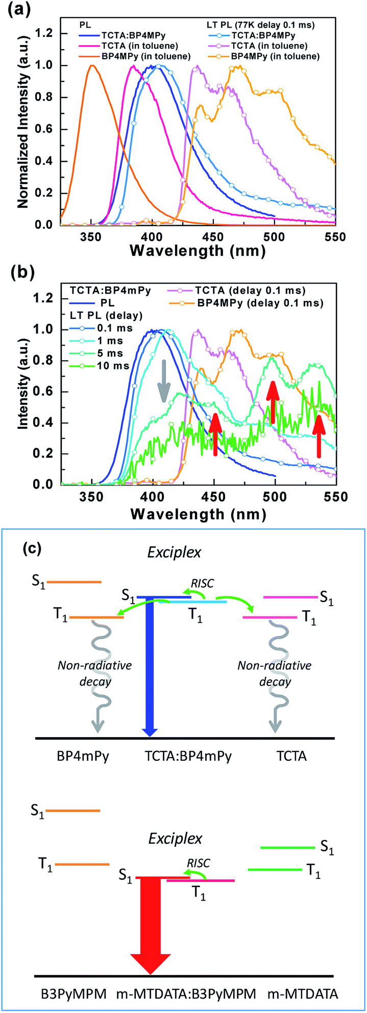 | ||
| Fig. 6 (a) Fluorescent and phosphorescent spectra of TCTA, BP4mPy, and sample B. (b) Phosphorescent spectra of sample B with different delay times. (c) The schematic diagram of energy transfers in samples B and R. | ||
| Materials | λmax. (nm) | FWHM (nm) | S1a (eV) | T1 (eV) | Lifetime | |
|---|---|---|---|---|---|---|
| Prompt (ns) | Decay (ns) | |||||
| a Estimated from the onset of the fluorescent spectrum.b Evaluated from the onset of the phosphorescent spectrum.c Collected from the previous reports (ref. 17, 20 and 21). | ||||||
| TCTA | 385 | 42 | 3.42 | 2.92b | 1.9 | n.d. |
| BP4mPy | 351 | 37 | 3.77 | 2.94b | 10.6 | n.d. |
| m-MTDATA | 424 | 46 | 3.11 | 2.65c | 1.8 | n.d. |
| TmPyPB | 349 | 38 | 3.29 | 2.75c | 11.3 | n.d. |
| B3PyMPM | 343 | 45 | 4.01 | 2.70c | 2.6 | n.d. |
| TCTA:BP4mPy (50:50) |
399 | 56 | 3.41 | 3.31b | 5.3 | n.d. |
| m-MTDATA:TmPyPB (80:20) |
483 | 106 | 3.08 | 3.03b | 27.5 | 105.1 |
| m-MTDATA:B3PyMPM (10:90) |
616 | 142 | 2.37 | 2.36b | 28.2 | 175.7 |
Conclusions
In conclusion, we propose a specific device architecture for WOLEDs without any molecular emitter, realizing a pure exciplex emission generated by the mixed HTMs/ETMs layers. Each red, green, and blue emission could be obtained by combining the appropriate HTM and ETM. Furthermore, a bipolar buffer layer was inserted between the green and red EMLs to adjust the carrier distribution and thus alter the emission. As a result, the corresponding CIE coordinates varies along with the Planckian locus as bias increases, realizing that WOLEDs imitate daylight. Furthermore, photophysical results indicate that the HTM/ETM used to produce exciplex should possess a higher triplet energy bandgap than that of the exciplex, thus avoiding energy loss to the composed single molecules.Conflicts of interest
The authors declare no conflict of interest.Acknowledgements
The authors gratefully acknowledge financial support from the Ministry of Science and Technology of Taiwan. (MOST 106-2221-E-155-035).References
- A. Endo, M. Ogasawara, A. Takahashi, D. Yokoyama, Y. Kato and C. Adachi, Adv. Mater., 2009, 21, 4802 CrossRef PubMed.
- A. Endo, K. Sato, K. Yoshimura, T. Kai, A. Kawada, H. Miyazaki and C. Adachi, Appl. Phys. Lett., 2011, 98, 083302 CrossRef.
- H. Uoyama, K. Goushi, K. Shizu, H. Nomura and C. Adachi, Nature, 2012, 492, 234 CrossRef PubMed.
- K. Goushi, K. Yoshida, K. Sato and C. Adachi, Nat. Photonics, 2012, 6, 253 CrossRef.
- W.-Y. Hung, G.-C. Fang, Y.-C. Chang, T.-Y. Kuo, P.-T. Chou, S.-W. Lin and K.-T. Wong, ACS Appl. Mater. Interfaces, 2013, 5, 6826 CrossRef PubMed.
- W.-Y. Hung, P.-Y. Chiang, S.-W. Lin, W.-C. Tang, Y.-T. Chen, S.-H. Liu, P.-T. Chou, Y.-T. Hung and K.-T. Wong, ACS Appl. Mater. Interfaces, 2016, 8, 4811 CrossRef PubMed.
- J. Li, H. Nomura, H. Miyazaki and C. Adachi, Chem. Commun., 2014, 50, 6174 RSC.
- X.-K. Liu, Z. Chen, C.-J. Zhang, C.-L. Liu, C.-S. Lee, F. Li, X.-M. Ou and X.-H. Zhang, Adv. Mater., 2015, 27, 2378 CrossRef PubMed.
- W. Liu, J.-X. Chen, C.-J. Zheng, K. Wang, D.-Y. Chen, F. Li, Y.-P. Dong, C.-S. Lee, X.-M. Ou and X.-H. Zhang, Adv. Funct. Mater., 2016, 26, 2002 CrossRef.
- S.-J. He, D.-K. Wang, N. Jiang, J. S. Tse and Z.-H. Lu, Adv. Mater., 2016, 28, 649 CrossRef PubMed.
- K.-H. Kim, S.-J. Yoo and J.-J. Kim, Chem. Mater., 2016, 28, 1936 CrossRef.
- W.-Y. Hung, T.-C. Wang, P.-Y. Chiang, B.-J. Peng and K.-T. Wong, ACS Appl. Mater. Interfaces, 2017, 9, 7355 CrossRef PubMed.
- D. Luo, Y. Xiao, M. Hao, Y. Yang, Y. Gao and B. Liu, Appl. Phys. Lett., 2017, 110, 061105 CrossRef.
- B. Liu, H. Nie, X. Zhou, S. Hu, D. Luo, D. Gao, J. Zou, M. Xu, L. Wang, Z. Zhao, A. Qin, J. Peng, H. Ning, Y. Cao and B.-Z. Tang, Adv. Funct. Mater., 2016, 26, 776 CrossRef.
- B. Liu, H. Tao, L. Wang, D. Gao, W. Liu, J. Zou, M. Xu, H. Ning, J. Peng and Y. Cao, Nano Energy, 2016, 26, 26 CrossRef.
- B. Liu, H. Nie, G. Lin, S. Hu, D. Gao, J. Zou, M. Xu, L. Wang, Z. Zhao, H. Ning, J. Peng, Y. Cao and B.-Z. Tang, ACS Appl. Mater. Interfaces, 2017, 9, 34162 CrossRef PubMed.
- J.-H. Jou, M.-H. Wu, S.-M. Shen, H.-C. Wang, S.-Z. Chen, S.-H. Chen, C.-R. Lin and Y.-L. Hsieh, Appl. Phys. Lett., 2009, 95, 013307 CrossRef.
- J.-H. Jou, C.-Y. Hsieh, J.-R. Tseng, S.-H. Peng, Y.-C. Jou, J. H. Hong, S.-M. Shen, M.-C. Tang, P.-C. Chen and C.-H. Lin, Adv. Funct. Mater., 2013, 23, 2750 CrossRef.
- J.-H. Jou, R.-Z. Wu, H.-H. Yu, C.-J. Li, Y.-C. Jou, S.-H. Peng, Y.-L. Chen, C.-T. Chen, S.-M. Shen, P. Joers and C.-Y. Hsieh, ACS Photonics, 2014, 1, 27 CrossRef.
- D. Luo, X.-L. Li, Y. Zhao, Y. Gao and B. Liu, ACS Photonics, 2017, 4, 1566 CrossRef.
- D. Luo, Q. Chen, Y. Gao, M. Zhang and B. Liu, ACS Energy Lett., 2018, 3, 1531 CrossRef.
- M. Huang, B. Jiang, G. Xie and C. Yang, J. Phys. Chem. Lett., 2017, 8, 4967 CrossRef PubMed.
- W. Song, H.-L. Lee and J.-Y. Lee, J. Mater. Chem. C, 2017, 5, 5923 RSC.
- S.-J. Su, D. Tanaka, Y.-j. Li, H. Sasabe, T. Takeda and J. Kido, Org. Lett., 2008, 10, 941 CrossRef PubMed.
- S.-J. Su, Y. Takahashi, T. Chiba, T. Takeda and J. Kido, Adv. Funct. Mater., 2009, 19, 1260 CrossRef.
- J.-H. Lee, S.-H. Cheng, S.-J. Yoo, H. Shin, J.-H. Chang, C.-I. Wu, K.-T. Wong and J.-J. Kim, Adv. Funct. Mater., 2015, 25, 361 CrossRef.
- S.-J. Su, H. Sasabe, T. Takeda and J. kido, Chem. Mater., 2008, 20, 1691 CrossRef.
- B. Zhao, H. Zhang, Y. Miao, Z. Wang, L. Gao, H. Wang, Y. Hao and W. Li, J. Mater. Chem. C, 2018, 6, 304 RSC.
- S. Wang, X. Wang, B. Yao, B. Zhang, J. Ding, Z. Xie and L. Wang, Sci. Rep., 2015, 5, 12487 CrossRef PubMed.
- E. Angioni, M. Chapran, K. Ivaniuk, N. Kostiv, V. Cherpak, P. Stakhira, A. Lazauskas, S. Tamulevicius, D. Volyniuk, N. J. Findlay, T. Tuttle, J. V. Grazulevicius and P. J. Skabara, J. Mater. Chem. C, 2016, 4, 3851 RSC.
- C.-H. Chang, C.-C. Chen, C.-C. Wu, S.-Y. Chang, J.-Y. Hung and Y. Chi, Org. Electron., 2010, 11, 266 CrossRef.
- C.-H. Chang, K.-C. Tien, C.-C. Chen, M.-S. Lin, H.-C. Cheng, S.-H. Liu, C.-C. Wu, J.-Y. Hung, Y.-C. Chiu and Y. Chi, Org. Electron., 2010, 11, 412 CrossRef.
- B. Liu, M. Xu, L. Wang, H. Tao, Y. Su, D. Gao, L. Lan, J. Zou and J. Peng, Nano-Micro Lett., 2014, 6, 335 CrossRef.
- B. Liu, D. Luo, J. Zou, D. Gao, H. Ning, L. Wang, J. Peng and Y. Cao, J. Mater. Chem. C, 2015, 3, 6359 RSC.
- B. Liu, X.-L. Li, H. Tao, J. Zou, M. Xu, L. Wang, J. Peng and Y. Cao, J. Mater. Chem. C, 2017, 5, 7668 RSC.
- S. Hofmann, M. Furno, B. Lussem, K. Leo and M. C. Gather, Phys. Status Solidi A, 2013, 8, 1467 CrossRef.
- D.-G. Chen, T.-C. Lin, C.-L. Chen, Y.-T. Chen, Y.-A. Chen, G.-H. Lee, P.-T. Chou, C.-W. Liao, P.-C. Chiu, C.-H. Chang, Y.-J. Lien and Y. Chi, ACS Appl. Mater. Interfaces, 2018, 10, 12886 CrossRef PubMed.
- C.-H. Chang, S.-W. Wu, C.-W. Huang, C.-T. Hsieh, S.-E. Lin, N.-P. Chen and H.-H. Chang, Jpn. J. Appl. Phys., 2017, 56, 129209 CrossRef.
- T. Lin, T. Zhang, Q. Song, F. Jin, Z. Liu, Z. Su, Y. Luo, B. Chu, C. S. Lee and W. Li, Org. Electron., 2016, 38, 69 CrossRef.
- S. Yuan, X. Du, J. Zhao, W. Liu, H. Lin, C. Zheng, S. Tao and X. Zhang, Org. Electron., 2016, 39, 10 CrossRef.
- H. Lim, H. Shin, K.-H. Kim, S.-J. Yoo, J.-S. Huh and J.-J. Kim, ACS Appl. Mater. Interfaces, 2017, 9, 37883 CrossRef PubMed.
Footnote |
| † Electronic supplementary information (ESI) available. See DOI: 10.1039/c8ra04986f |
| This journal is © The Royal Society of Chemistry 2018 |