 Open Access Article
Fabrication and characterization of distinctive ZnO/ZnS core–shell structures on silicon substrates via a hydrothermal method
Chin-Chi Chenga,
Wei Chih Wengb,
Hsueh I Linb,
Jo Lun Chiub,
Hong-Yu Jhaob,
Yu Ting Amber Liaoc,
Chang Tze Ricky Yuc and
Hsiang Chen *b
*b
aDepartment of Energy and Refrigerating Air-Conditioning Engineering Taipei, National Taipei University of Technology, Taiwan, Republic of China
bDepartment of Applied Materials and Optoelectronic Engineering, National Chi Nan University, Taiwan, Republic of China. E-mail: hchen@ncnu.edu.tw; Fax: +886-49-2912238; Tel: +886-49-2910960
cDepartment of Applied Chemistry, National Chi Nan University, Taiwan, Republic of China
First published on 24th July 2018
Abstract
A distinctive novel ZnO/ZnS core–shell structure on silicon was reported in this study. Compared with previous studies, ZnO nanorods encapsulated by 5 nm ZnS nanograins were observed using a scanning electron microscope. Furthermore, strong (111) cubic ZnS crystalline structures were confirmed using high resolution transmission electron microscopy, selected area diffraction, and X-ray diffraction. The optical properties changed and the antibacterial behaviors were suppressed as the ZnS shells were attached onto the ZnO nanorods. Moreover, the results also indicate that the hydrophobicity could be enhanced as more ZnS nanograins were wrapped onto the ZnO nanorods. The ZnO/ZnS core–shell structures in this research show promise for use in future optoelectronic and biomedical applications.
1. Introduction
Owing to the wide direct bandgap properties of ZnS and ZnO compound materials,1 nanostructures formed by ZnO and ZnS have drawn significant attention for their distinctive short wavelength optical applications and special catalyst properties.2–4 Recently, nanogeometries incorporating ZnS and ZnO with various geometric designs including nanorods,5,6 nanoparticles,7 hollow structures,8 core–shell structures,9–12 and Janus structures have been intensively studied.13,14 Among these nanostructures, ZnO/ZnS core–shell structures have attracted special attention because of their distinguished optical, piezoelectric15 and gas sensing16 properties caused by their distinctive ZnO/ZnS band diagrams and interfaces.17,18 Moreover, ZnO/ZnS core–shell structures can be synthesized via simple, low cost, fast fabrication and eco-friendly methods.16,19 For the aforementioned applications, ZnO/ZnS nanostructures have been deposited on various substrates such as ITO,20 GaN,18 and silicon substrates.21 Among these substrates, ZnO/ZnS on silicon substrates have the potential for future integration with silicon-based electronics or silicon-photonics. So far, some researchers have successfully formed these ZnO/ZnS nanostructures on silicon substrates, for example, Zhang et al. fabricated ZnS nanoforests/ZnO nanorods on silicon.22In addition, Kumarakuru et al. synthesized a uniform ZnS shell coating on ZnO nanorods.23 Modulating or tuning ZnS morphologies and material properties on ZnO nanorods may be useful for optimizing ZnO/ZnS-based nanodevices for future applications. Therefore, designing novel distinctive nanostructures for future potential utilization is worthwhile. In this study, 5 nm grain-like ZnS shells were formed and attached onto ZnO nanorods. In order to characterize the ZnO/ZnS nanostructures, several measuring instruments and testing technologies, such as field-emission scanning electron microscopy (FESEM), atomic force microscopy (AFM), transmission electron microscopy (TEM), X-ray diffraction (XRD), selected area diffraction (SAED), energy dispersive spectroscopy (EDS), photoluminescence (PL) spectroscopy, contact angle measurement and OD 600 tests, were utilized. The results indicate that the ZnO/ZnS nanostructures on silicon substrates with special morphologies and material properties are promising for future use in optoelectronic,10,24–27 biomedical,28–30 and catalytic applications.31,32
2. Experiments
To synthesise grain-like ZnS on ZnO/Si structures, silicon wafers were first cut into 2 cm × 2 cm substrates. Then, the silicon substrates were cleansed using the regular radio corporation of America (RCA) cleaning process. The ZnO seed layer was spin coated onto the silicon substrates with a lab-made solution. Then, ZnO nanorods were grown hydrothermally on the silicon substrates at 80 °C for one hour. The details of the solution and procedures can be seen in our previous works.21,33,34 After the cleaning and drying processes, the silicon substrates coated with ZnO nanorods were placed in a solution containing 0.05 M sulfide nanohydrate at 70 °C for 0, 5, 10, 20, and 30 minutes to form ZnO/ZnS structures on silicon. To characterize the ZnO/ZnS nanostructures, field-emission scanning electron microscopy (FESEM) and atomic force microscopy (AFM) were used to examine the surface morphologies. A transmission electron microscope (TEM) was used to observe the nanoshapes of ZnS on the ZnO nanorods. The crystallinity was analyzed using X-ray diffraction (XRD) and selected area diffraction (SAED). The element compositions in various locations were examined using energy dispersive spectroscopy (EDS). Furthermore, the optical, hydrophobic, and antibacterial properties were evaluated using photoluminescence (PL) spectroscopy, contact angle measurement, and OD 600 tests. The OD 600 test indicates the optical density of a sample measured at a wavelength of 600 nm. It is a common method for estimating the concentration of bacteria or other cells in a liquid. In this study, ZnO/ZnS nanostructures from various sulfurizing periods were bathed in bottles with Escherichia coli solution for 225 minutes. Then, the absorbance rate of the samples with respect to a light wavelength of 600 nm were measured using a photoelectric colorimeter.3. Results and discussion
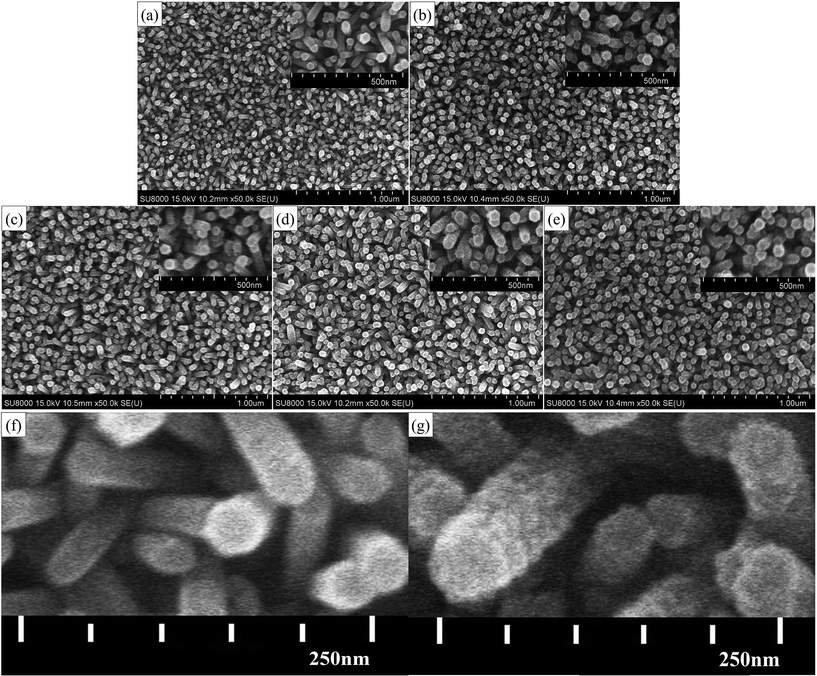
To examine the surface morphologies of the ZnO/ZnS core–shell structures, FESEM was used to observe the ZnS nanograins on the ZnO nanorods from the various sulfurization times of 0, 5, 10, 20 and 30 minutes, the results of which are shown in Fig. 1(a), (b), (c), (d) and (e), respectively. FESEM images with enlarged magnification rates are shown as the insets in the top-right of the these images. In Fig. 1(a), well-grown and densely populated ZnO nanorods with diameters around 40 nm can be observed. After the ZnO nanorods were sulfurized in a Na2S solution, ZnO/ZnS core–shell structures were formed and the surface of the nanorods became rougher. As the sulfurization time increased to 5 and 10 minutes, the ZnS nanograins became more apparent on the images. However, as the sulfurization time increased from 10 to 20 or 30 minutes, the surface of the ZnO nanorods became smoother again, as shown in Fig. 1(d) and (e). Therefore, the optimal sulfurization time to form ZnO/ZnS core–shell structures might be 10 minutes. Furthermore, enlarged FESEM images of the ZnO nanorods without a shell and ZnO nanorods with a ZnS shell are shown in Fig. 1(f) and (g). As can be seen by comparing Fig. 1(f) and (g), the thickness of ZnS ranged from 7 nm to 17 nm. It seems that the growth of ZnS nanograins might reach a saturated state when the sulfurization time exceeds 10 minutes. This may result from the saturated sulfurized reactions between ZnO and ZnS. The chemical reaction formulas are shown below:| ZnO + 2(OH)− ⇌ ZnO22− + H2O | (1) |
| ZnO22− + S2− + 2H2O ⇌ ZnS + 4(OH)− | (2) |
Compared with ZnO/ZnS core–shell structures on silicon, Zhang et al. fabricated ZnS nanoforests on ZnO nanorods as one type of ZnO/ZnS core–shell structure, as shown in Fig. 2(a). In addition, Kumarakuru et al. designed a ZnS sparsely distributed nanopowder on ZnO nanorods as another type of ZnO/ZnS core–shell structure, as shown in Fig. 2(b). In this study, with different fabrication methods, ZnS nanograins of around 5 nm were densely deposited on ZnO nanorods as ZnO/ZnS core–shell structures, as shown in Fig. 2(c).
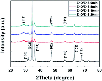
Moreover, to investigate the crystallization phase of the ZnO/ZnS nanostructures, XRD was used to explore the crystallinity, and the results are shown in Fig. 3. In Fig. 3, all the diffraction peaks are compared with information from the Joint Committee on Powder Diffraction Standards (JCPDS) table. For the ZnO nanorods without sulfurization, only ZnO phases can be observed (JCPDS. 792205). As the sulfurization time was increased to 5, 10 and 20 minutes, the cubic sphalerite (111) ZnS phases appeared (JCPDS. 790043).35
The ZnO/ZnS core–shell structures with a sulfurization time of 10 minutes had the strongest (111) ZnS phase and the narrowest half-maximum width among all the XRD patterns. According to Scherrer’s equation, the ZnS structure with 10 minutes of sulfurization might have the largest particle size among all of the sulfurized samples, which is consistent with the findings from the FESEM images.
In addition, AFM measurements were performed to study the surface roughness, and the results are shown in Fig. 4. The ZnO/ZnS core–shell structures with a sulfurization time of 0, 5, 10, 20 and 30 minutes had an average surface roughness (Ra) of 29.3, 31.2, 36.2, 34.6 and 31.9 nm, respectively, as shown in Fig. 4. These results are consistent with the findings of the FESEM images and XRD patterns, indicating that the ZnO/ZnS nanostructures with a sulfurization time of 10 minutes had the largest ZnS nanograins.
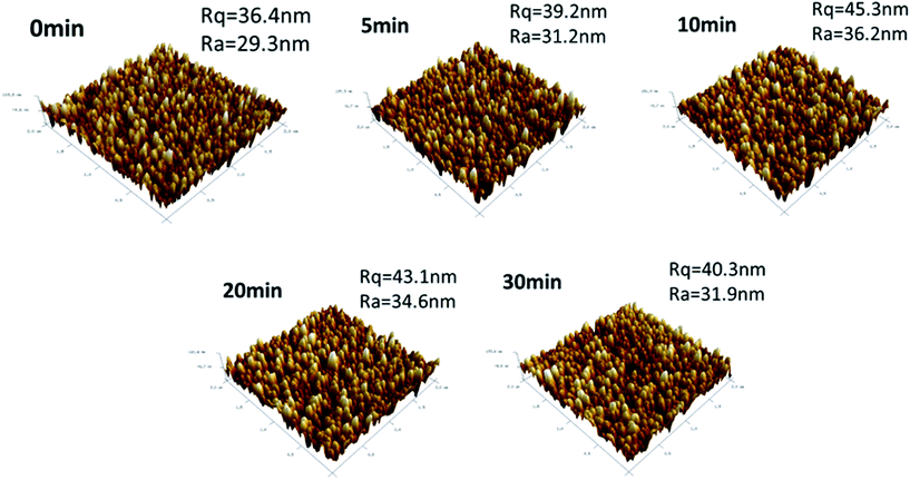 | ||
| Fig. 4 Atomic force microscopy (AFM) images of the ZnO/ZnS core–shell structures following various sulfurization periods. | ||
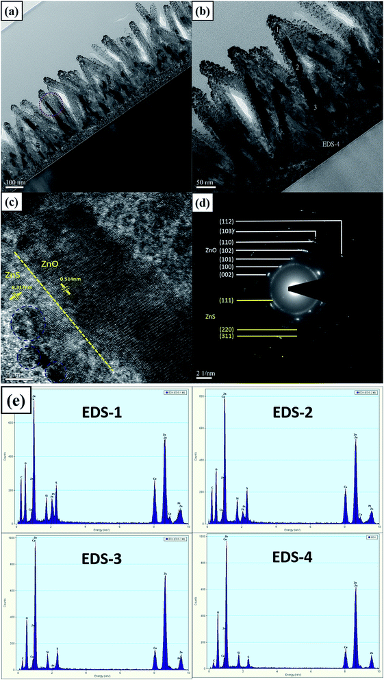
To zoom in on the surface morphology and detailed nanostructure of the ZnO/ZnS core–shell structures with a sulfurization time of 10 min, TEM, HRTEM, and SAED were utilized. TEM images with two different magnification rates are shown in Fig. 5(a) and (b), and ZnS nanograins distributed on the surface of ZnO nanorods can be clearly seen in the images. Moreover, a HRTEM image around the interface of ZnO/ZnS was taken and is shown in Fig. 5(c), and circular-shaped ZnS nanograins with radii of around 5 nm are noted by blue-dotted circles. The HRTEM image clearly presents the border between ZnS and ZnO, as illustrated by a dotted yellow line. Furthermore, the crystalline spacings between ZnO and ZnS were 0.514 nm and 0.317 nm, which correspond with previous studies.31 An SAED image shows all of the detailed ZnS and ZnO crystalline structures that are shown in the red-dotted circle in Fig. 5(a). A strong ZnS (111) ring is shown in the SAED image in Fig. 5(d). In addition, all of the patterns of the ZnO structures, including the strongest one of (002), are shown in the image. Moreover, two weak (220) and (311) ZnS structures can be observed in the HRTEM image, but the two structures are masked in the XRD patterns. Furthermore, to analyze the element composition on a single ZnO/ZnS nanorod composite, EDX was performed on a rod shown in Fig. 5(b) labeled 1 (top), 2 (upper level), 3 (bottom level), and 4 (bottom). The EDX results show that the strongest sulfur content was seen on the top, where many ZnS nanograins were found. Around the upper level labeled (2), less sulfur content was present. However, a strong sulfur signal could still be observed. As the location moved downward to the ZnO nanorod core, less sulfur content could be observed, indicating that little sulfur could diffuse to the core. Finally, with the location on the bottom (labeled (4), the ZnO seed layer), even less sulfur could be moved to the seed layer. The EDX analysis indicates that the sulfur might be diffused from the upper parts to the lower parts.
In addition to the surface morphologies and material characterizations, all these ZnO/ZnS core–shell structures were characterized with regards to their optical behaviors, surface hydrophilic properties and antibacterial capabilities.
The crystal defects and optical properties of the ZnO/ZnS core–shell structures were detected using photoluminescence (PL) spectroscopy. The measured results are presented in Fig. 6(a). In Fig. 6(a), the near-band-edge (NBE) ZnO peak around 380 nm indicates the recombination of the excitation energy caused by ultraviolet light. The visible light emission in the region between 500 and 600 nm is due to oxygen vacancies. After sulfurization, the oxygen vacancy defects were mitigated by the ZnS shells and the defect luminescence decreased. Moreover, a notable blue-shift of the NBE luminescence could be observed. The enlargement of the optical band-to-band transition is known as the Burstein–Moss effect. After the ZnO nanorods were doped with S to form ZnS, the S impurities contributed towards enhancing the electrical conductivity and thus resulted in a wider band-to-band transition, as shown in Fig. 6(b). Therefore, blue shifts of the band-to-band transitions could be viewed in the PL spectra.36
 | ||
| Fig. 6 (a) PL measurements of the ZnO/ZnS core–shell structures following various sulfurization periods. (b) Moss–Burstein shift mechanism diagram. | ||
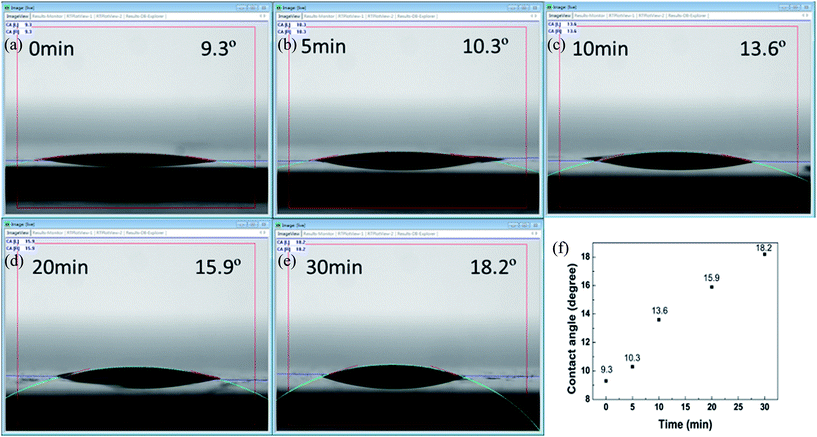
The hydrophobicity of the ZnO/ZnS core–shell structures following various sulfurization periods was analyzed using surface contact angle measurements, and the results are shown in Fig. 7(a)–(e). The surface contact angles of the ZnO/ZnS core–shell structures with a sulfurization time of 0, 5, 10, 20, and 30 minutes were 9.3, 10.3, 13.6, 15.9 and 18.2 degrees, respectively. These results indicate that a longer sulfurization time resulted in stronger hydrophobic properties. Therefore, ZnO/ZnS core–shell structures could be used for future waterproofing applications.21
Finally, the antibacterial abilities of the ZnO/ZnS core–shell structures were evaluated using the OD 600 antibacterial test. This test measured the absorbance rate of the samples with respect to a light wavelength of 600 nm using a photoelectric colorimeter. The absorbance rate of the sample with respect to a light wavelength of 600 nm was proportional to the concentration of bacteria. Six bottles were made up with the same solution, and one contained a control group while the other five contained the ZnO structures or ZnO/ZnS core–shell structures following various sulfurization periods. Each of these six samples were inserted into these bottles for 225 minutes, and the results are shown in Fig. 8. The results indicate that the samples with the ZnO or ZnO/ZnS core–shells had stronger antibacterial capabilities than the control group did, as shown in Fig. 8. The ZnO nanostructures improve the antibacterial capability37 due to their larger surface area and various morphologies, such as nanoparticles and 38 nanorods,39 H2O2 production, Zn2+ release, and the presence of surface oxygen vacancies.40 By examining Fig. 6(a), the oxygen vacancies, as revealed in the PL spectra, were increased. Therefore, the bacteria could be suppressed by the extra vacancies, which is consistent with the results of the antibacterial test shown in Fig. 8. Furthermore, compared with simple ZnO structures, a longer sulfurization time on the ZnO nanorods could weaken the antibacterial properties. Since the ZnO structures had superior antibacterial effects, the coating or coverage by the ZnS shells may block the contact between the ZnO nanorods and the bacteria. Therefore, the antibacterial effects could be suppressed.
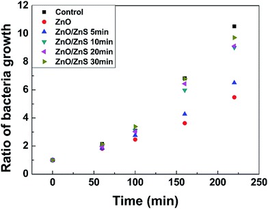 | ||
| Fig. 8 Ratio of bacteria growth versus the ZnO/ZnS core–shell structures following various sulfurization periods (OD 600 antibacterial test). | ||
4. Conclusions
Zinc sulfide (ZnS) nanograins were integrated onto zinc oxide (ZnO) rods to form distinctive ZnO/ZnS core–shell structures on silicon substrates. Multiple material characterizations were used to analyze these nanostructures. The results indicate that strong cubic crystallized ZnS (111) could be grown on ZnO nanorods following an appropriate sulfurization time. Furthermore, blue shifts of the PL spectra could be observed and the hydrophobicity could be enhanced with ZnS shell incorporation. Moreover, suppression of the antibacterial properties could be observed because of ZnS coverage on the ZnO nanorods. ZnO/ZnS core–shell structures on silicon substrates show promise for future applications related to Si-based electronic and biomedical nanodevices.Conflicts of interest
There are no conflicts to declare.Acknowledgements
This work has been supported in part by the Ministry of Science and Technology of Taiwan, ROC under Contract No: MOST 104-2221-E-260-002-MY3 and MOST 107-3113-E-008-003.References
- M. Oshikiri and F. Aryasetiawan, Phys. Rev. B: Condens. Matter Mater. Phys., 1999, 60, 10754 CrossRef.
- A. Sadollahkhani, O. Nur, M. Willander, I. Kazeminezhad, V. Khranovskyy, M. O. Eriksson, R. Yakimova and P.-O. Holtz, Ceram. Int., 2015, 41, 7174–7184 CrossRef.
- E. M. Flores, C. W. Raubach, R. Gouvea, E. Longo, S. Cava and M. L. Moreira, Mater. Chem. Phys., 2016, 173, 347–354 CrossRef.
- L. Yu, W. Chen, D. Li, J. Wang, Y. Shao, M. He, P. Wang and X. Zheng, Appl. Catal., B, 2015, 164, 453–461 CrossRef.
- X. Zhang, J. Qin, Y. Xue, P. Yu, B. Zhang, L. Wang and R. Liu, Sci. Rep., 2014, 4, 4596 CrossRef PubMed.
- Z. Chen, R. Wu, H. Wang, Y. Jiang, L. Jin, Y. Guo, Y. Song, F. Fang and D. Sun, Chem. Eng. J., 2017, 326, 680–690 CrossRef.
- W. He, H. Jia, J. Cai, X. Han, Z. Zheng, W. G. Wamer and J.-J. Yin, J. Phys. Chem. C, 2016, 120, 3187–3195 CrossRef.
- X. Huang, M.-G. Willinger, H. Fan, Z.-l. Xie, L. Wang, A. Klein-Hoffmann, F. Girgsdies, C.-S. Lee and X.-M. Meng, Nanoscale, 2014, 6, 8787–8795 RSC.
- H. Lin, L. Wei, C. Wu, Y. Chen, S. Yan, L. Mei and J. Jiao, Nanoscale Res. Lett., 2016, 11, 420 CrossRef PubMed.
- K. Wang, J. Chen, Z. Zeng, J. Tarr, W. Zhou, Y. Zhang, Y. Yan, C. Jiang, J. Pern and A. Mascarenhas, Appl. Phys. Lett., 2010, 96, 123105 CrossRef.
- S. C. Rai, K. Wang, Y. Ding, J. K. Marmon, M. Bhatt, Y. Zhang, W. Zhou and Z. L. Wang, ACS Nano, 2015, 9, 6419–6427 CrossRef PubMed.
- Y. Wang, X. Fang, R. Li, Y. Li, B. Yao, D. Wang, J. Tang, D. Fang, X. Wang and X. Wang, J. Mater. Sci.: Mater. Electron., 2018, 1–6 Search PubMed.
- J. Gong, X. Zu, Y. Li, W. Mu and Y. Deng, J. Mater. Chem., 2011, 21, 2067–2069 RSC.
- H. Shimose, M. Singh, D. Ahuja, W. Zhao, S. Shan, S. Nishino, M. Miyata, K. Higashimine, D. Mott and M. Koyano, J. Phys. Chem. C, 2016, 120, 5869–5875 CrossRef.
- S. Jeong, M. W. Kim, Y.-R. Jo, Y.-C. Leem, W.-K. Hong, B.-J. Kim and S.-J. Park, Nano Energy, 2016, 30, 208–216 CrossRef.
- X. Shuai and W. Shen, J. Phys. Chem. C, 2011, 115, 6415–6422 CrossRef.
- R. Li, Z. Wei, F. Zhao, X. Gao, X. Fang, Y. Li, X. Wang, J. Tang, D. Fang and H. Wang, Nanophotonics, 2017, 6, 1093 Search PubMed.
- X. Fang, Z. Wei, Y. Yang, R. Chen, Y. Li, J. Tang, D. Fang, H. Jia, D. Wang and J. Fan, ACS Appl. Mater. Interfaces, 2016, 8, 1661–1666 CrossRef PubMed.
- P. Chen, L. Gu and X. Cao, CrystEngComm, 2010, 12, 3950–3958 RSC.
- A. Brayek, M. Ghoul, A. Souissi, I. B. Assaker, H. Lecoq, S. Nowak, S. Chaguetmi, S. Ammar, M. Oueslati and R. Chtourou, Mater. Lett., 2014, 129, 142–145 CrossRef.
- T. Yu, K. Wang, Y. Chen, M. Sheu and H. Chen, Chalcogenide Lett., 2017, 14 Search PubMed.
- S. Zhang, B. Yin, H. Jiang, F. Qu, A. Umar and X. Wu, Dalton Trans., 2015, 44, 2409–2415 RSC.
- H. Kumarakuru, Z. N. Urgessa, E. J. Olivier, J. R. Botha, A. Venter and J. H. Neethling, J. Alloys Compd., 2014, 612, 154–162 CrossRef.
- X. Chen, Z. Bai, X. Yan, H. Yuan, G. Zhang, P. Lin, Z. Zhang, Y. Liu and Y. Zhang, Nanoscale, 2014, 6, 4691–4697 RSC.
- X. Fang, Z. Wei, R. Chen, J. Tang, H. Zhao, L. Zhang, D. Zhao, D. Fang, J. Li and F. Fang, ACS Appl. Mater. Interfaces, 2015, 7, 10331–10336 CrossRef PubMed.
- S. Sarkar, A. D. Mahapatra and D. Basak, J. Colloid Interface Sci., 2018, 523, 245–253 CrossRef PubMed.
- R. Li, Z. Wei, X. Fang, Y. Wang, Y. Li, D. Wang, J. Tang, D. Fang, X. Chu and B. Yao, ACS Appl. Nano Mater., 2018, 1, 1641–1647 CrossRef.
- S. Tarish, Y. Xu, Z. Wang, F. Mate, A. Al-Haddad, W. Wang and Y. Lei, Nanotechnology, 2017, 28, 405501 CrossRef PubMed.
- Y.-M. Sung, K. Noh, W.-C. Kwak and T. G. Kim, Sens. Actuators, B, 2012, 161, 453–459 CrossRef.
- A. Baranowska-Korczyc, K. Sobczak, P. Dłużewski, A. Reszka, B. J. Kowalski, Ł. Kłopotowski, D. Elbaum and K. Fronc, Phys. Chem. Chem. Phys., 2015, 17, 24029–24037 RSC.
- W. Chen, H. Ruan, Y. Hu, D. Li, Z. Chen, J. Xian, J. Chen, X. Fu, Y. Shao and Y. Zheng, CrystEngComm, 2012, 14, 6295–6305 RSC.
- M.-H. Hsu, C.-J. Chang and H.-T. Weng, ACS Sustainable Chem. Eng., 2016, 4, 1381–1391 CrossRef.
- T.-Y. Y. T.-Y. Yu, C. H. Hung, Y. S. Lee, C. F. Lin, W. M. Su, C.-C. Lu, C.-Y. Weng, Y. S. Wu, P. Y. Wu and H. Chen, J. New Mater. Electrochem. Syst., 2017, 20, 071–075 Search PubMed.
- T.-Y. Yu, M. R. Wei, C. Y. Weng, W. M. Su, C. C. Lu, Y. T. Chen and H. Chen, AIP Adv., 2017, 7, 065110 CrossRef.
- Y. Hu, H. Qian, Y. Liu, G. Du, F. Zhang, L. Wang and X. Hu, CrystEngComm, 2011, 13, 3438–3443 RSC.
- S. K. Panda, A. Dev and S. Chaudhuri, J. Phys. Chem. C, 2007, 111, 5039–5043 CrossRef.
- A. Azam, A. S. Ahmed, M. Oves, M. S. Khan, S. S. Habib and A. Memic, Int. J. Nanomed., 2012, 7, 6003 CrossRef PubMed.
- Z. Emami-Karvani and P. Chehrazi, Afr. J. Microbiol. Res., 2011, 5, 1368–1373 Search PubMed.
- K. Tam, A. Djurišić, C. Chan, Y. Xi, C. Tse, Y. Leung, W. Chan, F. Leung and D. Au, Thin Solid Films, 2008, 516, 6167–6174 CrossRef.
- R. K. Sharma, M. Agarwal and K. Balani, Mater. Sci. Eng. C, 2016, 62, 843–851 CrossRef PubMed.
| This journal is © The Royal Society of Chemistry 2018 |

