DOI:
10.1039/C8RA04705G
(Paper)
RSC Adv., 2018,
8, 31830-31834
The adsorption state and the evolution of field emission properties of graphene edges at different temperatures
Received
1st June 2018
, Accepted 8th August 2018
First published on 12th September 2018
Abstract
We have studied the effects of adsorbates on the field emission (FE) properties of graphene edges at different temperatures using Joule heating. Using infrared imaging and spectral fitting, the temperature from room temperature to about 1000 K was measured accurately. It was found that adsorption induces the deviation of graphene edge field emission from the Fowler–Nordheim law and the noise of the field emission. The adsorbates are gradually desorbed with an increase in temperature, and are almost completely desorbed above about 500 K. The FE of graphene edges without adsorption is fairly consistent with the FN theory.
1. Introduction
Since the field emission (FE) of carbon nanotubes (CNTs) was demonstrated,1 researchers have taken tremendous interest in the FE of low-dimensional carbon materials due to their unique structure, and excellent mechanical and chemical properties.1–16 Graphene is of atomic thickness, and exhibits high electrical conductivity, mechanical flexibility, and strong thermal/chemical stability, which qualify it as a promising FE source. Li et al.13 reported the FE properties of graphene films with gas adsorbates and the results showed that except N2, adsorption of O2 and CO2 reduced the FE current of graphene films. Of the many theoretical and experimental studies on graphene, most of them have focused on the properties of graphene edges due to their unusual electronic properties.17–25 However, the properties of graphene edges are very easily influenced by adsorbates around the graphene. We have already26 studied the water adsorption of a graphene edge emitter by FE experiments and first principles simulations. However, the process of adsorption/desorption hasn’t been investigated in detail. In this paper, the effects of adsorption/desorption on graphene edges at different temperatures have been studied. It was found that the adsorbates will be gradually desorbed with an increase in temperature, and is almost completely desorbed above about 500 K. The FE of graphene edges without adsorption is fairly consistent with the FN theory.
2. Experimental results and discussion
In this work, graphene was prepared using the same method as in our previous paper.26 Fig. 1(a) shows a 5000× scanning electron microscopy (SEM) image of the graphene. We found that the graphene has numerous thin open edges and tips. The Raman spectrum excited by a 514 nm laser is shown in Fig. 1(b), where the high 2D peak verified that the sample was composed predominately of few-layer graphene.27 Fig. 1(c) shows a transmission electron microscopy (TEM) image of the graphene. It can be seen that the graphene has a sharp edge. The inset in Fig. 1(c) displays the selected area electron diffraction (SAED) pattern of the graphene. This proves that the graphene is few-layered. Fig. 1(d) shows a TEM image of the graphene at a smaller magnification.
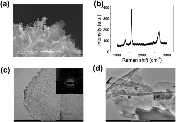 |
| | Fig. 1 (a) A scanning electron microscopy (SEM) image of the graphene; (b) Raman spectrum of the graphene excited by a 514 nm laser; (c) a transmission electron microscopy (TEM) image of the graphene at high magnification. Inset: The selected area electron diffraction (SAED) pattern of the graphene; (d) a transmission electron microscopy (TEM) image of the graphene at a smaller magnification. | |
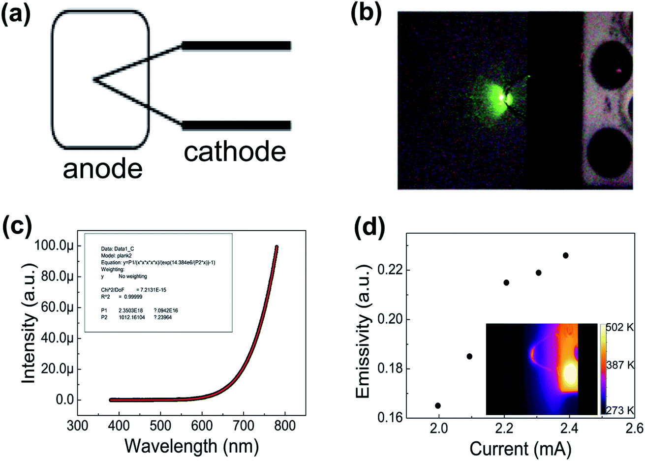
Fig. 2(a) shows a schematic diagram of the cathode and anode. The graphene field emitter was fabricated by sticking them on a molybdenum wire of 0.1 mm diameter with an organic binder, which can be thoroughly evaporated after being heated at 350 °C in air for a few minutes. An indium tin oxide (ITO) glass coated with phosphor was used as the anode. The anode was placed behind the cathode to avoid the effect of thermal expansion. The distance between the anode and cathode is about 200 μm. The FE experiment was conducted in a high-vacuum chamber with a base pressure of 10−5 Pa. Two metal rod electrodes were used to heat the graphene current passing through them. A Keithley 237 high voltage source measurement unit was used to supply the voltage, and Fig. 2(b) shows an image of the phosphor anode illuminated by the FE of the graphene cathode at 1100 V. Temperature is a very important physical quantity for the study of adsorption/desorption. The temperatures above 800 K were measured by optical spectral fitting. The emissivity of graphene is a necessary value when measuring temperature using the infrared imager. For the temperatures above 800 K, we firstly fit the spectra, and then measured the temperature with the infrared imager. Fig. 2(c) shows that the intensity changes with wavelength at 1012 K. The fitted curve is in good agreement with the measured value. This shows that temperature measurement by spectral fitting is very accurate.28 The temperatures below 800 K were measured by the infrared imager. The emissivity of the sample was adjusted when using the infrared imager so that the temperature was identical to that of the spectra fitting for temperatures above 800 K. The emissivity of the sample below 800 K was also adjusted following the same trends. Fig. 2(d) shows that the emissivity of the graphene changes with the current when the sample is heated. It can be seen that the emissivity of graphene increases with heating. The inset in Fig. 2(d) shows an image of the graphene at 383 K when the temperature was measured by the infrared imager. It also shows that the temperature can be measured by the thermal radiation spectrum.
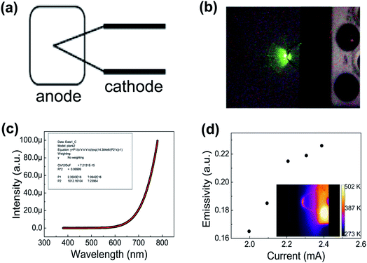 |
| | Fig. 2 (a) Schematic diagram of the cathode and anode; (b) image of the phosphor anode illuminated by the FE of the graphene; (c) the intensity change with wavelength at 1012 K; (d) the emissivity changes of graphene with current when the sample was heated. Inset: Image of the graphene sample at 383 K. | |
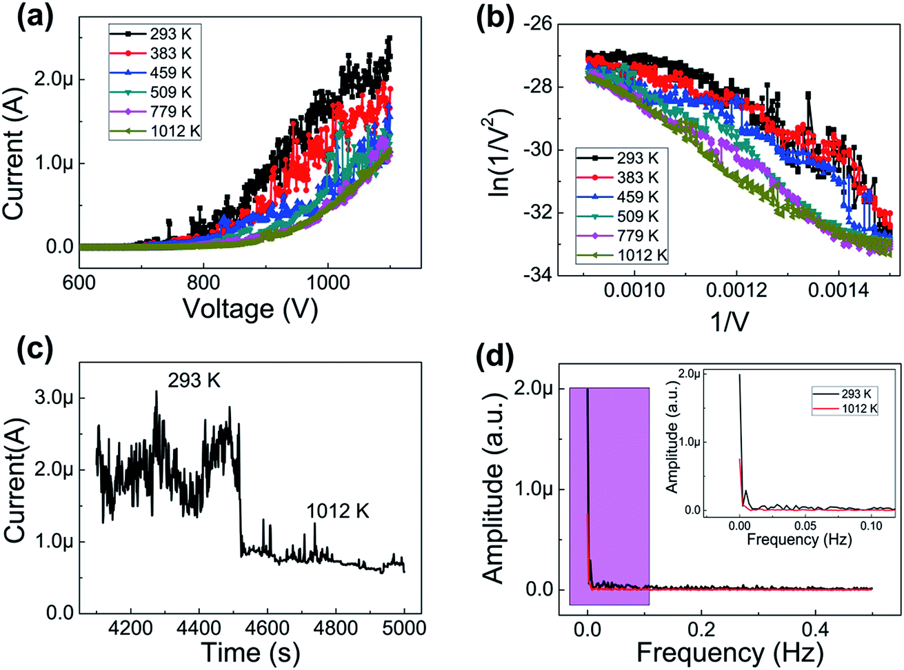
Fig. 3(a) shows the I–V curves of the graphene at different temperatures. Here, a DC voltage sweeping from 600 V to 1100 V was applied to the sample. It can be seen that the noise of the FE currents decreases with an increase in temperature. The turn-on (defined at emission current 0.1 μA) field and the biggest emission current are shown in Table 1. The biggest emission current is 2.4 μA at RT, 1.9 μA at 383 K, 1.5 μA at 459 K, 1.35 μA at 509 K, 1.3 μA at 779 K and 1.15 μA at 1012 K. This is mainly due to the fact that the FE of the graphene is influenced by the adsorption.29,30 The adsorbates are almost completely desorbed above 500 K. This shows that heating can be used as a useful method to remove adsorbates. The FE current was affected by adsorption/desorption, but these do not alter the inherent properties of the graphene FE emitter. The FE at 1012 K in this experiment was determined as the intrinsic FE of graphene after the complete removal of adsorbates. The emission current is 0.1 μA at 4.45 V μm−1 and 1.15 μA at 5.5 V μm−1. Fig. 3(b) displays the corresponding Fowler–Nordheim (FN) plots. It also shows that the noise of the FE current at 293 K is significantly higher than that at 1012 K. Fig. 3(d) displays the amplitude change with frequency by fast Fourier transform (FFT) at 293 K and 1012 K. It can be seen that the curve is very noisy at 293 K and the curve is very smooth at 1012 K. The FN equation31 is expressed as follows:
| |
 | (1) |
where
J is the current density,
λM is a macroscopic pre-exponential correction factor,
a and
b are constants (
a = 1.54 × 10
−6 A eV V
−2,
b = 6.83 eV
−3/2 V nm
−1),
ϕ is the work function of the emitter (4.74 eV for graphene
17),
E is the applied electric field
32 (
E =
V/
d, where
V is the voltage applied between the flat cathode and the anode screen and
d is their separation),
β is the local electrical field enhancement factor, and
vF (correction factor) is the Schottky–Nordheim barrier function. The field enhancement factor
β can be calculated from the slope (
m) of the FN curves (the curves of ln(1/
V2)
versus (1/
V), using the following equation.
| |
 | (2) |
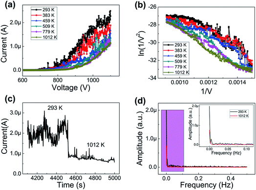 |
| | Fig. 3 (a) Field emission I–V curves of the graphene at different temperatures; (b) FN curves of the graphene at different temperatures; (c) field emission current change with time at 293 K and 1012 K; (d) the amplitude change with frequency by fast Fourier transform (FFT) at 293 K and 1012 K. | |
Table 1 The turn-on field, emission current, intercept, slope and ϕ of graphene at different temperatures
| |
Turn-on field (V/μm) |
Emission current (μA) |
Intercept |
Slope |
ϕ (eV) |
| 293 K |
3.6 |
2.4 |
−16.59773 |
−9997.86398 |
4.695 |
| 383 K |
3.85 |
1.9 |
−18.72544 |
−8380.30797 |
4.174 |
| 459 K |
3.92 |
1.5 |
−18.28973 |
−9224.39898 |
4.450 |
| 509 K |
4.15 |
1.35 |
−16.54843 |
−11![[thin space (1/6-em)]](https://www.rsc.org/images/entities/char_2009.gif) 237.04029 237.04029 |
5.076 |
| 779 K |
4.3 |
1.3 |
−17.93949 |
−10370.27289 |
4.811 |
| 1012 K |
4.5 |
1.15 |
−18.43309 |
−10142.22375 |
4.74 |
To further prove the influence of adsorption on the graphene, the FE current change with time at 293 K and 1012 K is shown in Fig. 3(c). It can be seen that the FE current at 293 K is higher than the FE current at 1012 K.
Fig. 4(a)–(c) shows the calculated intercept, slope and ϕ at different temperature. The field-enhancement factor (β) of graphene was calculated to be about 6900 at 1012 K. The large β shows that graphene is an excellent field emitter. As adsorption does not change the geometric structure of graphene, β at low temperatures can be viewed as almost the same as that at high temperatures. The work function at different temperatures was calculated as listed in Table 1 by solving eqn (2) based on β and the slope of the FN plot between 0.001–0.0015 (670–1000 V). By selecting the slope of the FN plot at 0.001–0.0015, the intercept. It can be seen that ϕ increases with temperature at below 500 K. ϕ is basically the same when the temperature is above 500 K. This shows that the adsorbates are almost completely desorbed above 509 K, and the adsorption energy is about 44 meV.
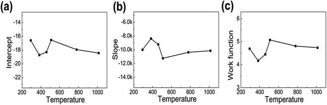 |
| | Fig. 4 The intercept, slope and work function (ϕ) of the graphene edge emitter at different temperatures. | |
3. Conclusions
In summary, the effect of adsorption on graphene edges at different temperatures has been demonstrated in detail. It is shown that the noise of the I–V and FN curves decreases with an increase in temperature. The noise of the I–V and FN curves is well explained by the adsorption effect. The adsorbates are almost completely desorbed above 500 K. It is shown that the intrinsic FE of the graphene follows the FN theory fairly well. The enhancement factor β was calculated to be about 6900 using the FN theory, and the large β makes graphene an interesting material for a wide variety of scientific and technological applications.
Conflicts of interest
There are no conflicts to declare.
Acknowledgements
This work is financed by the National Key R&D Program of China (Grant No. 2018YFA0208401 and 2017YFA0205800), NSFC (Grant No. 51572146, 51727805, and 51672152), the Beijing Advanced Innovation Center for Future Chip (ICFC), the Innovation Talents Program of Science and Technology of Institution of Higher Education of Henan Province, China (Grant No. 14HASTIT044), the Science and Technology Project of Henan Province, China (Grant No. 182102310884), and the Ninth Group of Key Disciplines in Henan province, China (Grant No. 2018119).
References
- W. A. de Heer, A. Chatelain and D. Ugarte, Science, 1995, 270, 1179–1180 CrossRef.
- S. S. Fan, M. G. Chapline, N. R. Franklin, T. W. Tombler, A. M. Cassell and H. J. Dai, Science, 1999, 283, 512–514 CrossRef PubMed.
- J. M. Bonard, J. P. Salvetat, T. Stockli, L. Forro and A. Chatelain, Appl. Phys. A: Mater. Sci. Process., 1999, 69, 245–254 CrossRef.
- J. M. Bonard, H. Kind, T. Stockli and L. O. Nilsson, Solid-State Electron., 2001, 45, 893–914 CrossRef.
- Y. Cheng and O. Zhou, C. R. Phys., 2003, 4, 1021–1033 CrossRef.
- S. C. Lim, K. Lee, I. H. Lee and Y. H. Lee, Nano, 2007, 2, 69–89 CrossRef.
- C. H. Weng, K. C. Leou, H. W. Wei, Z. Y. Juang, M. T. Wei, C. H. Tung and C. H. Tsai, Appl. Phys. Lett., 2004, 85, 4732–4734 CrossRef.
- G. Y. Zhang, X. Jiang and E. G. Wang, Appl. Phys. Lett., 2004, 84, 2646–2648 CrossRef.
- C. L. Tsai, C. F. Chen and L. K. Wu, Appl. Phys. Lett., 2002, 81, 721–723 CrossRef.
- R. Che, M. Takeguchi, M. Shimojo and K. Furuya, J. Phys.: Conf. Ser., 2007, 61, 200–204 CrossRef.
- L. R. Baylor, V. I. Merkulov, E. D. Ellis, M. A. Guillorn, D. H. Lowndes, A. V. Melechko, M. L. Simpson and J. H. Whealton, J. Appl. Phys., 2002, 91, 4602–4606 CrossRef.
- Y. H. Wu, B. J. Yang, B. Y. Zong, H. Sun, Z. X. Shen and Y. P. Feng, J. Mater. Chem., 2004, 14, 469–477 RSC.
- J. Li, X. B. Yan, G. Y. Gou, Z. Wang and J. T. Chen, Phys. Chem. Chem. Phys., 2014, 16, 1850–1855 RSC.
- R. Khare, D. B. Shinde, S. Bansode, M. A. More, M. Majumder, V. K. Pillai and D. J. Late, Appl. Phys. Lett., 2015, 106, 0231111–0231115 CrossRef.
- A. K. Samantara, D. K. Mishra, S. R. Suryawanshi, M. A. More, R. Thapa, D. J. Late, B. K. Jena and C. S. Rout, RSC Adv., 2015, 5, 41887–41893 RSC.
- P. K. Bankar, S. S. Warule, S. R. Jadkar, N. S. Chaudhari and M. A. More, RSC Adv., 2016, 6, 83084–83090 RSC.
- F. Zhu, X. Y. Lin, P. Liu, K. L. Jiang, Y. Wei, Y. Wu, J. P. Wang and S. S. Fan, Nano Res., 2014, 7, 553–560 CrossRef.
- C. Ö. Girit, J. C. Meyer, R. Erni, M. D. Rossell, C. Kisielowski, L. Yang, C. H. Park, M. F. Crommie, M. L. Cohen, S. G. Louie and A. Zettl, Science, 2009, 323, 1705–1708 CrossRef PubMed.
- B. Huang, M. Liu, N. H. Su, J. Wu, W. H. Duan, B. L. Gu and F. Liu, Phys. Rev. Lett., 2009, 102, 166404–166412 CrossRef PubMed.
- K. Suenaga and M. Koshino, Nature, 2010, 468, 1088–1090 CrossRef PubMed.
- Y. Kobayashi, K. I. Fukui and T. Enoki, Phys. Rev. B: Condens. Matter Mater. Phys., 2006, 73, 125415–125422 CrossRef.
- M. Fujita, K. Wakabayashi, K. Nakada and K. Kusakabe, J. Phys. Soc. Jpn., 1996, 65, 1920–1923 CrossRef.
- K. Nakada, M. Fujita, G. Dresselhaus and M. S. Dresselhaus, Phys. Rev. B: Condens. Matter Mater. Phys., 1996, 54, 17954–17961 CrossRef.
- L. Yang, C. H. Park, Y. W. Son, M. L. Cohen and S. G. Louie, Phys. Rev. Lett., 2007, 99, 1868011–1868014 Search PubMed.
- Y. W. Son, M. L. Cohen and S. G. Louie, Nature, 2006, 444, 347–349 CrossRef PubMed.
- L. J. Jiang, J. L. Wang, P. Liu, W. Song and B. L. He, RSC Adv., 2018, 8, 11216–11221 RSC.
- R. Saito, M. Hofmann, G. Dresselhaus, A. Jorio and M. S. Dresselhaus, Adv. Phys., 2011, 60, 488–503 CrossRef.
- P. Li, K. L. Jiang, M. Liu, Q. Q. Li, S. S. Fan and J. L. Sun, Appl. Phys. Lett., 2003, 82, 1763–1765 CrossRef.
- L. W. Swanson and A. E. Bell, Adv. Electron. Electron Phys., 1973, 32, 193–309 Search PubMed.
- P. Liu, K. L. Jiang, Y. Wei, K. Liu, L. Liu and S. S. Fan, J. Vac. Sci. Technol., B: Microelectron. Nanometer Struct.--Process., Meas., Phenom., 2010, 28, 736–739 CrossRef.
- R. H. Fowler and L. Nordheim, Proc. R. Soc. A, 1928, 119, 173–181 CrossRef.
- R. G. Forbes, Nanotechnology, 2012, 23, 0957061–09570612 Search PubMed.
|
| This journal is © The Royal Society of Chemistry 2018 |
Click here to see how this site uses Cookies. View our privacy policy here. 
 Open Access Article
 This Open Access Article is licensed under a Creative Commons Attribution-Non Commercial 3.0 Unported Licence
 ab,
Peng Liu*b,
Lina Zhangb,
Changhong Liub,
Liwei Zhanga and
Shoushan Fanb
ab,
Peng Liu*b,
Lina Zhangb,
Changhong Liub,
Liwei Zhanga and
Shoushan Fanb