
 Open Access Article
 This Open Access Article is licensed under a Creative Commons Attribution-Non Commercial 3.0 Unported Licence
Flaky nano-crystalline SnSe2 thin films for photoelectrochemical current generation†
Xiuyuan Shao‡
 *a,
Shisheng Li‡*abc and
Dai-Ming Tangc
*a,
Shisheng Li‡*abc and
Dai-Ming Tangc
aDepartment of Physics, National University of Singapore, 6 Science Drive 2, 117546, Singapore. E-mail: xiuyuan_shao@u.nus.edu
bCentre for Advanced 2D Materials, National University of Singapore, 2 Science Drive 3, 117542, Singapore
cInternational Center for Materials Nanoarchitectonics (MANA), National Institute for Materials Science (NIMS), Namiki 1-1, Tsukuba, Ibaraki 305-0044, Japan. E-mail: LI.Shisheng@nims.go.jp
First published on 17th September 2018
Abstract
We report chemical vapor deposition (CVD) and photoelectrochemical properties of large-area thin films of nano-crystalline SnSe2 on conducting FTO glass. We show that densely packed, randomly oriented SnSe2 nanoflakes can be grown by reacting vapors of tin monoselenide (SnSe) and selenium at 550 °C without compromising the electrical properties of FTO. We demonstrate that SnSe2/FTO is photoelectrochemically active in visible to near-UV wavelengths (350–700 nm) and exhibits incident-photon-to-current-efficiency (IPCE) as high as 3.7% at 0 V versus the Ag/AgCl/1 M KCl reference electrode under 350 nm light illumination.
Introduction
Photoelectrochemical cells (PECs) convert solar energy into electrical power by photo-induced electrochemical reactions at semiconductor–electrolyte interfaces.1–3 Layered chalcogenide materials (LCMs) such as MoS2 and WSe2 have been considered as ideal materials for photoelectrochemical devices for a long time due to the formation of an electrocatalytically active interface with the electrolytes.4–7 PECs with promising performance have been demonstrated with bulk crystals and thin films of a variety of LCMs.8–12Recent surges of interests in this class of materials have led to remarkable advances in the optoelectronics of ultrathin LCM sheets.13,14 Monolayer sheets of group VI transition metal dichalcogenides have been extensively studied due to their direct band gap and wide-range light-absorption properties.15 The strong light–matter interaction and their extremely large surface-to-volume ratio make them attractive for applications in photocatalysis and photoelectrochemical applications.16 In order to translate these attractive properties of LCMs into cell performance, it is essential to fabricate a film consisting of high-quality flakes and high surface area. Liquid exfoliation17–20 and solvothermal synthesis21,22 of LCMs hold promise for large-scale production, however these methods have been found to lead to many defects and a small crystal size. Crystal edges and surface defects are considered to be recombination centers for excitons and thus, large crystal domains with low defect density are needed for PEC applications. Recent studies show that monolayer MoS2 flakes prepared by chemical exfoliation21 and SnSe2 flakes synthesized by solvothermal method22 exhibit low incident-photon-to-current-efficiency (IPCE) of ∼1%, most likely due to the limited crystal quality and the limited effective surface area. Thus, a method to fabricate large-area thin films with high surface area needs to be developed. Towards this end, chemical vapor deposition (CVD) offers a simple, controllable and scalable route to produce high-quality 2D crystals with desired morphologies.
Tin diselenide (SnSe2) is an earth-abundant layered dichalcogenide and a promising candidate as the photoanode of PECs due to its suitable band gap (indirect bandgap ∼1 eV, and direct bandgap ∼1.5 eV at 300 K).23 In contrast to other LCMs, CVD-grown nanostructured SnSe2 has rarely been explored, impeding extensive explorations of PECs based on this material. Here, we present a facile low-temperature CVD growth of centimeter-scale thin films consisting of randomly oriented SnSe2 nanoflakes on FTO glass. We show that the as-grown SnSe2 thin film on FTO glass can be used as a photoanode for PECs. The SnSe2/FTO electrodes exhibit excellent IPCE values as high as 3.7% conducted at 0 V potential against Ag/AgCl/1 M KCl reference electrode, significantly higher than the reported values for chemically prepared nanosheets of MoS2 and SnSe2.20,21
Fig. 1a shows the configuration of our CVD set up. Similar to the previous study,24 selenium source was placed in the low-temperature upstream region and tin monoselenide (SnSe) powder was placed at the center of the furnace to generate SnSe vapor. A cleaned FTO glass was loaded in the low-temperature downstream (∼300–350 °C) of the quartz tube. Growth was conducted at 550 °C and in ∼1 torr Argon atmosphere. After the growth, a semitransparent gray film was deposited on the FTO glass (inset of Fig. 1b). The film is typically uniform across the ∼1.5 × 2.0 cm2 FTO glass. Four-probe test indicates that the surface resistance of FTO-coated glass increased from ∼25 ohms (Ω) to ∼180 Ω after the growth of SnSe2. The high surface conductivity of SnSe2/FTO comes from the high electron mobility of SnSe2 and the robust bonding between SnSe2 nanoflakes and FTO glass (ESI Fig. S1†). It should be noted that the deposited SnSe2 film is mostly a reaction product of Se and SnSe rather than the selenization of FTO. The combination of high electrical conductivity and the optical bandgap of ∼1.64 eV make the flaky SnSe2 ideal for PECs (ESI Fig. S2†).
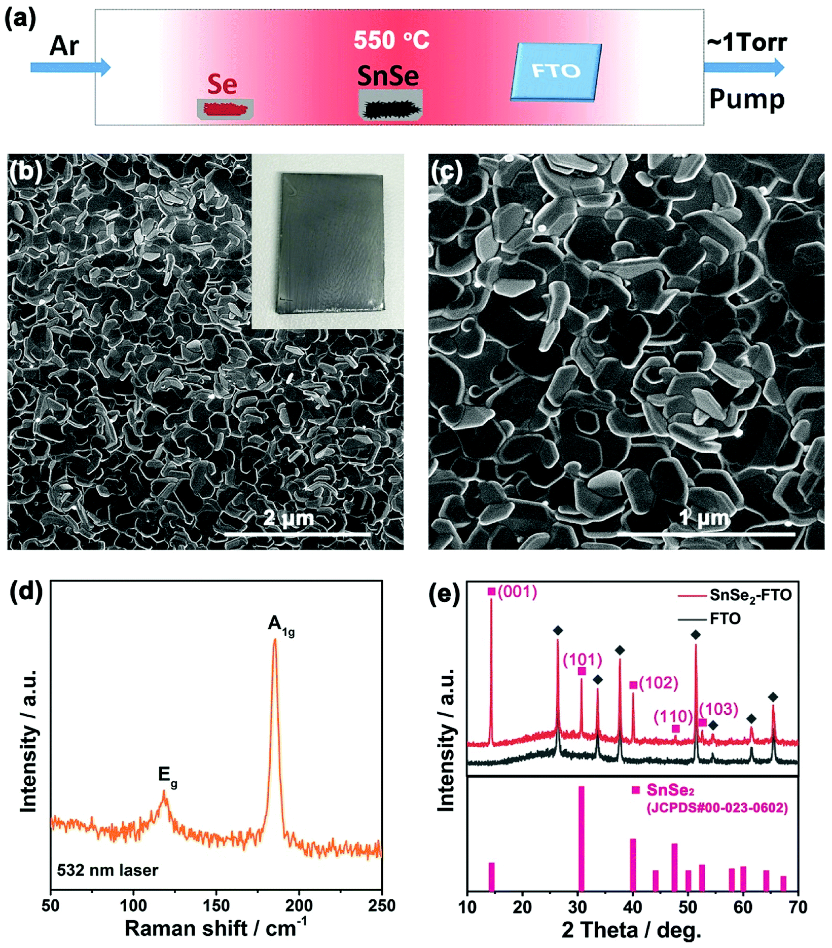 | ||
| Fig. 1 (a) Schematic illustration of the growth set up. (b and c) SEM images of as-grown SnSe2 nanoflakes on FTO glass. Inset of (b) is an optical image of SnSe2/FTO glass. (d) Raman spectrum of as-grown SnSe2 nanoflakes with 532 nm excitation laser. (e) XRD patterns for SnSe2/FTO glass and bare FTO glass. Bottom trace represents the powder diffraction patterns for SnSe2 standard. | ||
Fig. 1b and c are scanning electron microscopy (SEM) images of as-grown SnSe2 nanoflakes on FTO glass. The SnSe2 nanoflakes have a uniform coverage on the FTO glass. The magnified image demonstrates the as-grown SnSe2 nanoflakes have a hexagonal shape with a lateral size from several tens to several hundred nanometers. This was also verified by the transmission electron microscopy (TEM) as demonstrated in Fig. 2a. The thickness of these SnSe2 nanoflakes is 38.1 ± 13.7 nm. All the as-grown SnSe2 nanoflakes are tilted and well bonded to the FTO glass, forming a porous 3D nanostructure (ESI Fig. S2†). The tilted and porous structure of SnSe2 nanoflakes and their robust connection to the FTO glass provide high-speed channels for both ion diffusion and electron transportation, which make SnSe2/FTO a good candidate for applications of PECs.25
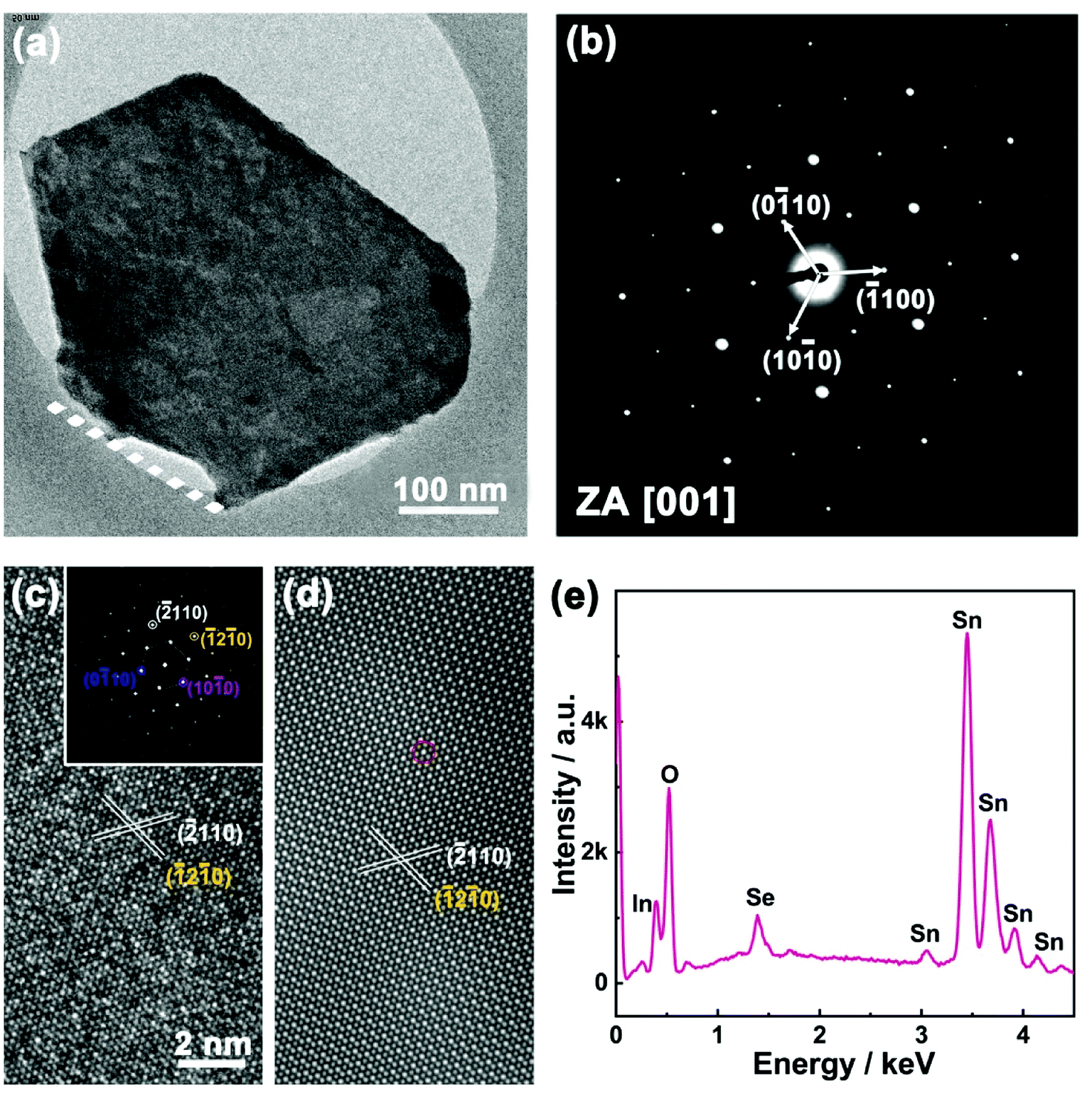 | ||
| Fig. 2 (a) TEM image of a SnSe2 nanoflake. (b) SAED pattern of the SnSe2 nanoflake. (c) High-resolution TEM image of the SnSe2 nanoflake. Inset is the corresponding fast Fourier transform (FFT) from the TEM image along [001] zone axis. (d) Inverse FFT image of the SnSe2 nanoflake. (e) EDX spectrum of a SnSe2 nanoflake grown on FTO glass. | ||
Fig. 1d shows a representative unpolarized Raman spectrum of the as-grown SnSe2 nanoflakes on FTO glass. Two strong peaks located at 118.3 cm−1 and 185.6 cm−1 are assigned to Eg (in-plane) and A1g (out-plane) Raman active modes, respectively.3–5 Fig. 1e shows the X-ray diffraction (XRD) patterns for SnSe2/FTO and FTO glass. After the deposition of SnSe2 nanoflakes on FTO glass, there are five new peaks located at 14.40°, 30.71°, 40.08°, 47.60°, 52.61° and 42.15° that can be observed. These five peaks can be assigned to the (001), (101), (102), (110) and (103) crystal planes of hexagonal SnSe2 (JCPDS. no. 00-023-0602), respectively. The predominant (001) peak of SnSe2 is attributed to the preferential growth along the (001) basal plane of SnSe2 nanoflakes.
The quality of as-grown 2D SnSe2 nanoflakes has been further examined by the selected area electron diffraction (SAED), the high-resolution TEM imaging and the energy dispersive X-ray spectroscopy (EDX). For TEM characterization, the as-grown SnSe2 nanoflakes were scratched from the FTO glass. We found the SnSe2 nanoflakes cannot be removed from the FTO glass even by high power ultra-sonication, revealing the strong bonding between SnSe2 nanoflakes and the FTO substrates. Fig. 2a is a TEM image of one isolated SnSe2 nanoflake on a TEM grid. The as-grown SnSe2 nanoflakes have a hexagonal shape with a lateral size of several hundred nanometers. Only one side of the SnSe2 nanoflakes (dashed line in Fig. 2a) is bonded with FTO glass. Fig. 2b is the SAED pattern of the SnSe2 nanoflake, which signifies its single-crystalline nature with an in-plane lattice constant of a = b = 0.38 nm, which is consistent with previous results of bulk SnSe2.24–26 The hexagonally symmetric SAED pattern is in excellent agreement with the hexagonal crystal structure of SnSe2 nanoflakes (P3m1), and the zone axis is assigned to the [001] direction. The high-resolution TEM image and its corresponding fast Fourier transform (FFT) of the SnSe2 nanoflake are demonstrated in Fig. 2c and inset, respectively. The SnSe2 nanoflake with an interplanar spacing of 0.19 nm was indexed to the (−2110) planes. Fig. 2d is the inverse FFT of SnSe2 nanoflakes based on the inset FFT pattern in Fig. 2c. It reveals more clearly the atomic arrangement of Sn and Se elements in the hexagonal crystal structure. In the inverse FFT image the bright dots indicated by the red circle represent Sn atoms due to its high atomic number, while the dark dots represent Se atoms. EDX spectrum and mapping further confirm the elemental uniformity over the whole nanoflakes (Fig. 2e, ESI Fig. S3 and S4†).
As a proof-of-concept application, the SnSe2/FTO electrode was assembled into a PEC as illustrated in ESI Fig. S5† and depicted in experimental section with more details. Fig. 3a shows the linear sweep voltammograms of SnSe2/FTO electrode, where the black and red curves represent the current density under the “OFF” state (constant dark environment) and the “ON” state (under constant white light illumination), respectively. The linear sweep voltammograms of the bare FTO glass was conducted to confirm the magnitude of photocurrent and to exclude the contribution from the FTO substrate (ESI Fig. S6†). The corresponding switched ON/OFF photocurrent at 0 V applied potential across the cell is shown in the Fig. 3b. These results exhibit good switching and reproducible behaviors with chopped visible light illumination, where the response time (including both the rising and decay time) was found to be nearly at 80 milliseconds. All the SnSe2/FTO samples produce positive photocurrent with the magnitude of the generated current increasing gradually with increasing the applied potential (Fig. 3b), and hence the SnSe2 belong to an n-type semiconductor.21 The immediate rise of photocurrent from OFF to ON state proves that such SnSe2 nanoflake-based photoanode is very sensitive to the visible light illumination. This is because the SnSe2 nanoflake with a small bandgap is able to effectively absorb the visible light. It is worth noting that the overshooting behavior of the photocurrent can be clearly observed when switching on the light. This may be attributed to the accumulation of photogenerated electrons at the SnSe2 nanoflake–electrolyte interface, which subsequently recombine with holes until a steady photocurrent is reached.
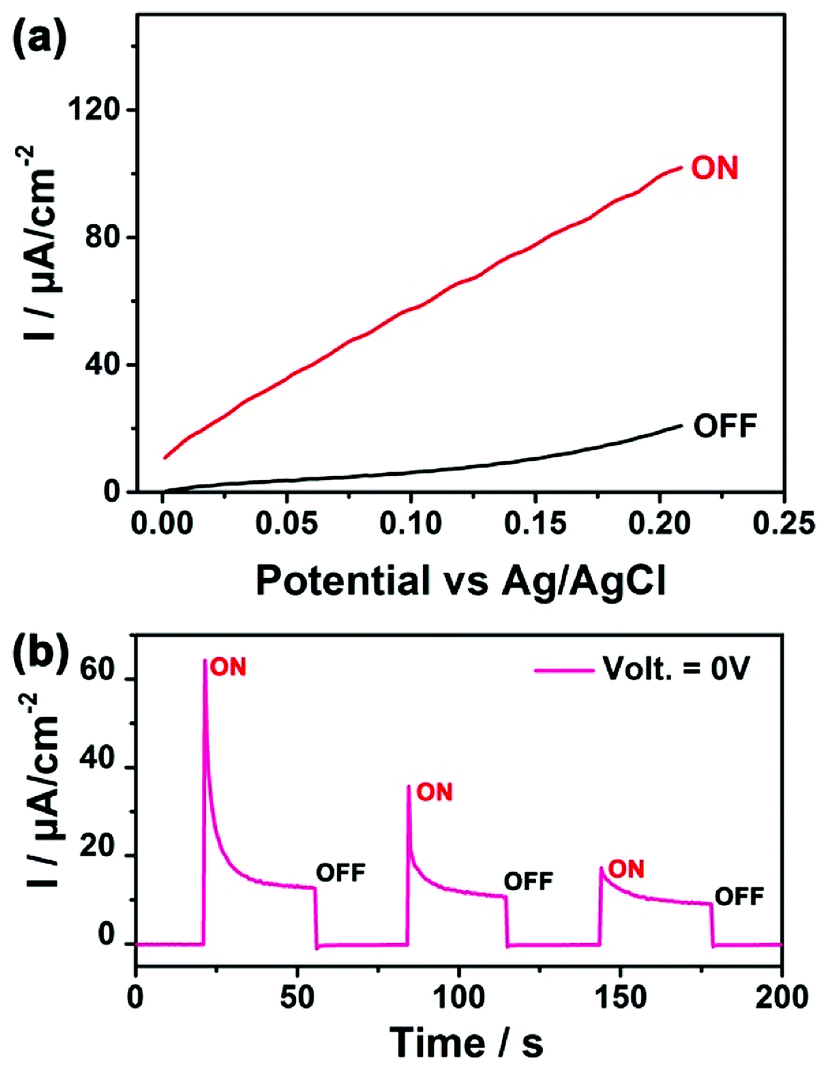 | ||
| Fig. 3 (a) Linear sweep voltammograms of SnSe2/FTO electrode in dark and under illumination at the applied voltage between 0 V and 0.2 V versus Ag/AgCl electrode. (b) A typical current–time curve at 0 V versus Ag/AgCl electrode. | ||
To further demonstrate the conversion efficiency of light, especially in the visible lights region, the transient current under chopped illumination of light for SnSe2/FTO PEC at 0 V bias across the cell was measured under the chopped illumination of light with a wavelength ranging from 350 nm to 700 nm with a step of 10 nm. Fig. 4a–c show that the photocurrent can be reproducibly switched between “ON” state and “OFF” state by periodically turn the light on and off, which indicates fast photoresponse characteristics as well as wide spectrum responses in the visible light region. The decay of photocurrent in a continuous running is negligible, demonstrating that the SnSe2 nanoflakes as photoanodes are relatively stable in the photo-oxidation process. Moreover, the relative low dark current (∼10 nA) and high photocurrent (∼70 nA) also guarantee an outstanding optical switching performance.
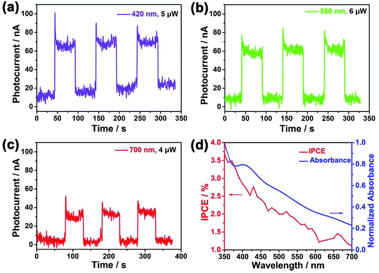 | ||
| Fig. 4 Time-dependent photoresponse of SnSe2 PEC under the illumination of selected wavelengths at the potential of 0 V vs. Ag/AgCl: (a) 700 nm, 4 μW; (b) 550 nm, 6 μW; (c) 420 nm, 5 μW. (d) Plot of IPCE spectrum (red line) and absorbance spectrum (blue line) versus wavelength at the potential of 0 V vs. Ag/AgCl electrode. | ||
IPCE is a key parameter to evaluate the quantum yield photocurrent efficiencies, and IPCE is defined as the incident-photon-to-current-efficiency:
 | (1) |
The photocurrent generation process in a PEC results from charge carrier generation, separation and recombination at the semiconductor–electrolyte interface. A space charge layer is usually built when the solid semiconductor in contact with a liquid electrolyte since their initial chemical potential of electrons is different (Fig. 5a). The chemical potential of the semiconductor is determined by the Fermi level while the chemical potential is identified as the redox potential of the redox couples for the electrolyte. In the case of n-type SnSe2 thin films contacted with 0.5 M Na2SO4 aqueous solution, which gives an equilibrium potential at about 0.33 V vs. NHE. The proximity to the OER redox potential gives a similar degree of band bending at the SnSe2 thin film/electrolyte interface. Fig. 5b shows the schematic energy band diagram for SnSe2 photoanode in contact with the SO42−/SO32− redox couple in the dark. Upon the illumination of PEC, the photo-generated charge carriers at the SnSe2/electrolyte interface are separated by the electric field present in the space charge layer, as shown in Fig. 5c. Alternatively, the Pt counter electrode (CE) is aligned with the reversible redox level, while in the SnSe2 electrode the quasi Fermi level splits into electron Fermi level and hole Fermi level upon the illumination. The hole Fermi level again aligns with the redox couple, leading to the reduction open circuit potential (OCP) observed in the experiments. In photoelectrocatalysis, the greater the band-bending the faster the electron/hole separation occurs, and thus the recombination of charges is therefore minimized.30,31 Meanwhile, the SnSe2/FTO interface also helps in separating charge carriers by forming a p-type Schottky barrier (by knowing the work function, ϕSnSe2 = 5.3 eV and ϕFTO = 4.4 eV),32,33 retarding the recombination effect and extending the charge carrier lifetime, leading to an excellent photoresponse.
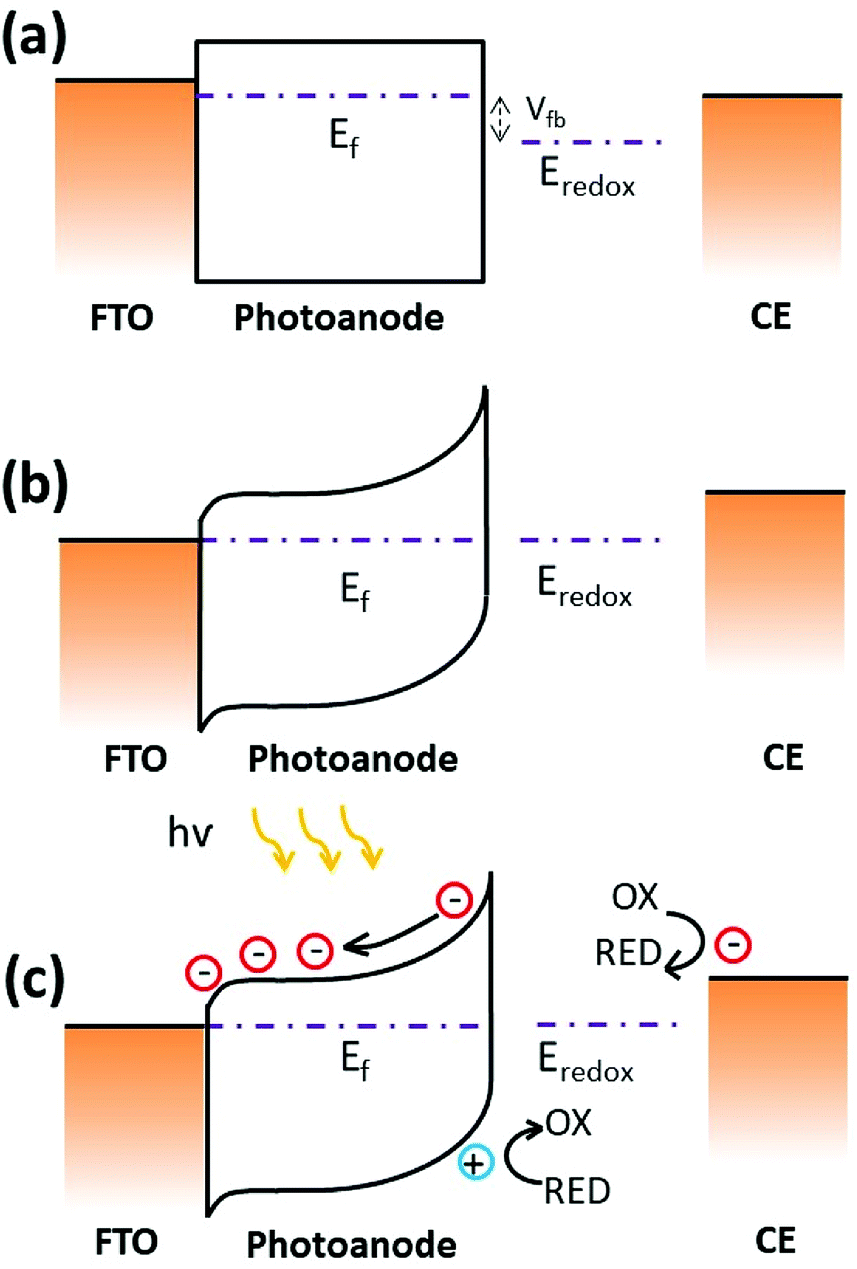 | ||
| Fig. 5 Schematic energy band diagrams for flat band potential (a), and for SnSe2 photoanode in contact with the SO42−/SO32− redox couple in the dark (b) and under illumination (c). Ef is the Fermi level energy. Eredox is the redox potential in the electrolyte (0.5 M Na2SO4). The counter electrode is Pt mesh. | ||
In conclusion, a simple and scalable CVD method was developed to grow tilted SnSe2 nanoflakes on FTO substrates. The SnSe2 with a suitable bandgap of ∼1.64 eV is an idea material for PEC applications in visible light range. The unique vertically oriented morphology further endows abundant semiconductor/electrolyte interfaces and catalytic edge sites. The robust connection between SnSe2 and FTO substrates also speeds up charge transportation in the SnSe2/FTO photoanode. This method is versatile and possible for scalable synthesis of other photoactive materials with this unique structure on conducting substrates.
Experimental section
Chemical vapor deposition of SnSe2 nanoflakes on FTO glass
A thermal furnace equipped with fused quartz tube was employed for growing SnSe2 nanoflakes on FTO glass. For a typical growth, ∼50 mg Se shot (99.999+%, Alfa Aesar) was loaded in the low temperature upstream (∼250 °C). ∼10 mg SnSe (99.995+%, Sigma-Aldrich) was loaded in an alumina crucible at the center of the quartz tube. Cleaned FTO glass with a size of ∼1.5 × 2.0 cm2 was put at low-temperature downstream (∼300–350 °C) for growing SnSe2 nanoflakes. The tube furnace was first flushed with 500 sccm Ar for 10 min. Then, the Ar flow rate was tuned to 25 sccm. The chamber pressure was pumped down to ∼1 torr to facilitate the sublimation of SnSe at 550 °C. The tube furnace was heated up with a ramping rate of 20 °C min−1 to 550 °C and the growth was held at 550 °C for ∼5 min. Finally, the furnace was cooled down to room temperature in Ar.TEM sample preparation
The SnSe2 nanoflakes were scratched from the FTO glass using blade. Then, the SnSe2 nanoflakes were dispersed in a drop of ethanol directly on the FTO glass. Copper grid with porous carbon film was immersed in the SnSe2/ethanol solution to capture the SnSe2 nanoflakes.Characterization of SnSe2 nanoflakes
The morphology, microstructure, and chemical composition of the SnSe2 nanoflakes were studied using scanning electron microscope (SEM, FEI Verios 460), transmission electron microscope (TEM, JEOL 3100FEF, 300 KeV), and X-ray powder diffraction (XRD, Philips X'Pert MPD). Raman spectra were obtained with a laser confocal microscope (NT-MDT, NTEGR Spectra) in back scattering geometry with 532 nm excitation laser.Photoelectrochemical test of SnSe2/FTO electrodes
Photoelectrochemical tests were carried out in an in-house built three-electrode cell fitted with fused silica windows at room temperature. A 250 W Xenon lamp and CM110 1/8 meter monochromator were used to illuminate the SnSe2/FTO electrodes. The exposed area for light irradiation is a circle with a diameter of 1 cm. All the currents were recorded by a program controlled Potentiostat, and all the measurements were conducted against an Ag/AgCl/1 M KCl reference electrode with a Pt mesh counter electrode. 0.5 M Na2SO4 aqueous solution was used as the electrolyte. The power intensity of individual wavelengths ranging from 350–700 nm was measured by a Thorlabs power meter.Conflicts of interest
The authors declare no competing financial interest.Acknowledgements
X. Shao and S. Li acknowledge Prof. Goki Eda for his support. Prof. Goki Eda acknowledges Singapore National Research Foundation for partly funding the research under its NRF Research Fellowship (NRF-NRFF2011-02).References
- A. Kargar, K. Sun, Y. Jing, C. Choi, H. Jeong, Y. Zhou, K. Madsen, P. Naughton, S. Jin and G. Y. Jung, Nano Lett., 2013, 13, 3017–3022 CrossRef PubMed.
- X. Yu, M. S. Prévot, N. Guijarro and K. Sivula, Nat. Commun., 2015, 6, 7596 CrossRef PubMed.
- X. Xu, J. Hu, Z. Yin and C. Xu, ACS Appl. Mater. Interfaces, 2014, 6, 5983–5987 CrossRef PubMed.
- H. Tributsch and J. C. Bennett, J. Electroanal. Chem. Interfacial Electrochem., 1977, 81, 97–111 CrossRef.
- F. R. F. Fan, H. S. White, B. L. Wheeler and A. J. Bard, J. Am. Chem. Soc., 1980, 102, 5142–5148 CrossRef.
- S. Z. Butler, S. M. Hollen, L. Cao, Y. Cui, J. A. Gupta, H. R. Gutierrez, T. F. Heinz, S. S. Hong, J. Huang, A. F. Ismach, E. Johnston-Halperin, M. Kuno, V. V. Plashnitsa, R. D. Robinson, R. S. Ruoff, S. Salahuddin, J. Shan, L. Shi, M. G. Spencer, M. Terrones, W. Windl and J. E. Goldberger, ACS Nano, 2013, 7, 2898–2926 CrossRef PubMed.
- W. J. Zhao, R. M. Ribeiro and G. Eda, Acc. Chem. Res., 2015, 48, 91–99 CrossRef PubMed.
- G. Kline, K. K. Kam, R. Ziegler and B. Parkinson, Sol. Energy Mater., 1982, 6, 337–350 CrossRef.
- J. Gobrecht, H. Tributsch and H. Gerischer, J. Electrochem. Soc., 1978, 125, 2085–2086 CrossRef.
- G. Kline, K. Kam, D. Canfield and B. Parkinson, Sol. Energy Mater., 1981, 4, 301–308 CrossRef.
- R. Audas and J. Irwin, J. Appl. Phys., 1981, 52, 6954–6960 CrossRef.
- R. Tenne and A. Wold, Appl. Phys. Lett., 1985, 47, 707–709 CrossRef.
- Q. H. Wang, K. Kalantar-Zadeh, A. Kis, J. N. Coleman and M. S. Strano, Nat. Nanotechnol., 2012, 7, 699–712 CrossRef PubMed.
- Y. Huang, K. Xu, Z. Wang, T. A. Shifa, Q. Wang, F. Wang, C. Jiang and J. He, Nanoscale, 2015, 7, 17375–17380 RSC.
- Z. Zeng, Z. Yin, X. Huang, H. Li, Q. He, G. Lu, F. Boey and H. Zhang, Angew. Chem., Int. Ed., 2011, 50, 11093–11097 CrossRef PubMed.
- N. D. Boscher, C. J. Carmalt, R. G. Palgrave and I. P. Parkin, Thin Solid Films, 2008, 516, 4750–4757 CrossRef.
- V. Nicolosi, M. Chhowalla, M. G. Kanatzidis, M. S. Strano and J. N. Coleman, Science, 2013, 340, 1226419 CrossRef.
- G. Cunningham, M. Lotya, C. S. Cucinotta, S. Sanvito, S. D. Bergin, R. Menzel, M. S. Shaffer and J. N. Coleman, ACS Nano, 2012, 6, 3468–3480 CrossRef PubMed.
- U. Halim, C. R. Zheng, Y. Chen, Z. Lin, S. Jiang, R. Cheng, Y. Huang and X. Duan, Nat. Commun., 2013, 4, 2213–2219 CrossRef PubMed.
- L. A. King, W. Zhao, M. Chhowalla, D. J. Riley and G. Eda, J. Mater. Chem. A, 2013, 1, 8935–8941 RSC.
- Z. Fang, S. Hao, L. Long, H. Fang, T. Qiang and Y. Song, CrystEngComm, 2014, 16, 2404–2410 RSC.
- X. Dai, Z. Li, K. Du, H. Sun, Y. Yang, X. Zhang, X. Ma and J. Wang, Electrochim. Acta, 2015, 171, 72–80 CrossRef.
- D. Martínez-Escobar, M. Ramachandran, A. Sánchez-Juárez and J. S. N. Rios, Thin Solid Films, 2013, 535, 390–393 CrossRef.
- L. Huang, Y. Yu, C. Li and L. Cao, J. Phys. Chem. C, 2013, 117, 6469–6475 CrossRef.
- S. Li, Y. Luo, W. Lv, W. Yu, S. Wu, P. Hou, Q. Yang, Q. Meng, C. Liu and H. M. Cheng, Adv. Energy Mater., 2011, 1, 486–490 CrossRef.
- E. Trifonova, Y. I. Yanchev, P. Manou, K. Kambas and N. A. Anagnostopoulos, J. Mater. Sci., 1996, 31, 3647–3649 CrossRef.
- Y. H. Ng, A. Iwase, A. Kudo and R. Amal, J. Phys. Chem. Lett., 2010, 1, 2607–2612 CrossRef.
- T. F. Jaramillo, K. P. Jørgensen, J. Bonde, J. H. Nielsen, S. Horch and I. Chorkendorff, Science, 2007, 317, 100–102 CrossRef PubMed.
- J. Kibsgaard, Z. Chen, B. N. Reinecke and T. F. Jaramillo, Nat. Mater., 2012, 11, 963–969 CrossRef PubMed.
- A. L. Linsebigler, G. Lu and J. T. Yates Jr, Chem. Rev., 1995, 95, 735–758 CrossRef.
- G. G. Bessegato, J. C. Cardoso, B. F. da Silva and M. V. B. Zanoni, J. Photochem. Photobiol., A, 2014, 276, 96–103 CrossRef.
- T. Shimada, F. S. Ohuchi and B. A. Parkinson, Jpn. J. Appl. Phys., 1994, 33, 2696–2698 CrossRef.
- A. Andersson, N. Johansson, P. Broms, N. Yu, D. Lupo and W. R. Salaneck, Adv. Mater., 1998, 10, 859–863 CrossRef.
Footnotes |
| † Electronic supplementary information (ESI) available. See DOI: 10.1039/c8ra04639e |
| ‡ X. Shao and S. Li contribute equally to this work. |
| This journal is © The Royal Society of Chemistry 2018 |