DOI:
10.1039/C8RA04582H
(Paper)
RSC Adv., 2018,
8, 20423-20433
Flexible resistive switching bistable memory devices using ZnO nanoparticles embedded in polyvinyl alcohol (PVA) matrix and poly(3,4-ethylenedioxythiophene) polystyrene sulfonate (PEDOT:PSS)†
Received
29th May 2018
, Accepted 29th May 2018
First published on 5th June 2018
Abstract
The resistive switching memory effects in metal-insulator-metal devices with aluminium (Al) as top electrode (TE) and bottom electrode (BE). A solution processed active layer consisting of zinc oxide (ZnO) nanoparticles embedded in an insulating polyvinyl alcohol (PVA) matrix and polymer poly(3,4-ethylenedioxythiophene) polystyrene sulfonate (PEDOT:PSS) has been studied by using flexible polyethylene terephthalate (PET) substrates. The current–voltage (I–V) measurements of hybrid Al/ZnO–PVA/PEDOT:PSS/Al/flexible PET substrate device exhibited a non-volatile bistable resistive switching behaviour, which is attributed to the trapping, storage and transport of charges in the electronic states of the ZnO nanoparticles. The performance of hybrid device is significantly enhanced over control Al/PEDOT:PSS/Al and Al/ZnO–PVA/Al devices due the presence of PEDOT:PSS polymer. This PEDOT:PSS improves the performance of oxygen ions (holes) migration toward BE and protect back oxygen vacancies (electrons) migrate toward BE from ZnO–PVA composites which may reduces the leakage current, as a result, increased the ‘ON state/OFF state’ current ratio of 7.9 × 10³ times. The fabricated hybrid device showed high ON/OFF switching current ratio larger than five orders of magnitude with low operating voltages. It is observed that, the existence of two conducting states, namely, low conductivity state (OFF state) and high conductivity state (ON state), exhibiting bistable behaviour. The state of the device was maintained even after removal of the applied bias, indicating the non-volatile memory. The observed current–time response showed good memory retention behaviour of the fabricated devices. The excellent stability and retention performances of hybrid device verify the reliability of this device and demonstrate their potential for application in non-volatile bistable memory device. The carrier transport mechanism of the bistable behaviour for the fabricated non-volatile organic bistable devices structures is described on the basis of the I–V experimental results by analyzing the effect of space charge and electronic structure. Interestingly, the device performance was not degraded and remains identical even after bending the device from 60–120° angles, which indicates high potential for flexible non-volatile bistable memory device applications. This demonstration provides a class of memory devices with the potential for future flexible electronics applications.
1. Introduction
A mixture of semiconductor nanoparticles and polymers has been particularly interesting due to their potential applications in next-generation electronic and optoelectronic devices.1–4 Nanocomposites containing semiconductor nanoparticles and polymer have promising potential applications in non-volatile memory devices due to their high mechanical flexibility, low cost, and simple fabrication.5–8 In memory devices based on nanocomposites, the electrical bistability is primarily determined by the semiconductor nanoparticles.9–11 The prospect of applications of non-volatile memory devices utilizing nanocomposites has given rise to extensive research and efforts to develop semiconductor nanoparticles, serving as charging and discharging islands, embedded in a polymer matrix.12–18 In the past decade, there are many kinds of advanced non-volatile memory devices have been generated.19,20 Among the several types of non-volatile memory devices, the hybrid non-volatile bistable devices have been particularly attractive due to their easier fabrication, less expensive and high flexibility without additional sources and drains.21–23 With the effort of analyzing current transport behaviour, many studies indicated that semiconductor nanoparticles in such memory devices are responsible for the charge trapping, storage, and emission induced current bistable effect.24 Among the various types of semiconductor nanoparticles, zinc oxide (ZnO) have acted as promising candidates because of their potential applications in non-volatile memory devices and their being environment friendly materials.25–29 ZnO is n-type semiconductors with a band-gap of 3.37 eV at 300 K. ZnO based thin film devices have good resistive switching characteristics. It has been extensively studied in both unipolar and bipolar resistive switching behaviour, such as Pt/ZnO/Pt,30 Al/ZnO/Si,31 TiN/ZnO/Pt,32 and Cr/ZnO/Pt.33 Metal/bilayer/metal structure was proposed to improve the performance of the resistive switching behaviour. Lee et al.,34 fabricated bilayer ZrOx/HfOx-based structure to improve resistive switching behaviour. It was observed that, the ‘HRS/LRS′′ ratio increased by 100 times compared to single HfOx-based structure. Although there are several reports for the growth of semiconductor nanostructures embedded in polyvinyl alcohol (PVA) polymer matrix, the realization of hybrid ZnO–PVA nanocomposites/conducting polymer model heterostructure used for flexible non-volatile bistable resistive switching memory devices has not been investigated earlier in details. A detail study is necessary for the fabrication of this model heterostructure for possible applications in flexible devices.
In this report, we fabricated and investigated flexible non-volatile bistable memory devices utilizing ZnO–PVA nanocomposites and conducting polymer poly(3,4-ethylenedioxythiophene) polystyrene sulfonate (PEDOT:PSS) on an aluminium (Al) coated flexible polyethylene terephthalate (PET) substrates. ZnO is highly suitable material to trap charge carriers due to its appropriate quantum confinement and available energy states. PVA is used as an isolating dielectric material and a supportive layer to transfer the nanoparticles onto the bottom electrodes. Furthermore, PVA is a biocompatible, non-toxic, low cost, environment friendly and non-hazardous organic polymer. PEDOT:PSS is a p-type hole conducting polymer which improved the resistive switching ON/OFF state current ratio of hybrid Al/ZnO–PVA/PEDOT:PSS/Al/flexible PET substrate device by improving the oxygen ions (holes) migration toward BE and protect back oxygen vacancies (electrons) transfer toward BE from ZnO–PVA nanocomposites, which may reduces the leakage current. This work was undertaken to comprehensively explore the resistive switching effect in a hybrid ZnO–PVA/PEDOT:PSS film model heterojunction system as being the potential candidate for the next generation memory device. The fabricated device exhibited a non-volatile and bistable resistive switching behaviour. The carrier transport mechanisms and organic bistable resistive switching behaviour of the ZnO–PVA/PEDOT:PSS model heterojunction system has been demonstrated for potential used in flexible devices.
2. Experimental details
2.1 Synthesis of ZnO nanoparticles
ZnO nanoparticles (NPs) were prepared using sol–gel method.35 In details, 0.01 M of zinc acetate (Merck, 99%) was dissolved in 2-propanal (Merck, 99%) followed by heating and stirring at 65 °C. After 30 minutes, diethanolamine (Nice, 99%) was added to the previous solution, and a transparent solution was achieved. The molar ratio of zinc acetate and diethanolamine was taken as 1![[thin space (1/6-em)]](https://www.rsc.org/images/entities/char_2009.gif) :2. The solution was kept for half an hour at room temperature. The as grown ZnO NPs were filtered out from the solution and dried in air for further applications.
:2. The solution was kept for half an hour at room temperature. The as grown ZnO NPs were filtered out from the solution and dried in air for further applications.
2.2 Preparation of ZnO–polyvinyl alcohol (PVA) nanocomposites
ZnO–PVA nanocomposite films were prepared by the well known solution casting technique. In this method, 4 gram of solid PVA (C2H4O)n (where n = 1700) was dissolved in 150 ml of de-ionized (DI) water by heating and stirring at ∼95 °C for 2 hours using a magnetic stirrer with hot plate, for complete dissolution without thermal decomposition of the polymer, until the polymer was completely dissolved and a clear viscous solution is formed. The prepared ZnO nanoparticle was added into the aqueous solution of PVA, and then stirred carefully by using magnetic stirrer until well dispersion ZnO–PVA was obtained. For electrical characterizations, different concentration ratios [ZnO NPs (mg):PVA solution (ml)] of 5:1, 8:1, 10:1, 15:1, and 25:1 have been studied. Sample with a concentration ratio of 10:1 shows superior electrical resistive switching behaviour compared to 5:1, 8:1, 15:1, and 25:1 samples, as shown in ESI Fig. SF1.†
2.3 Device fabrication
To produce the device structure, first, aluminum strips were deposited on flexible polyethylene terephthalate (PET) substrate by thermal evaporation through a shadow mask. Second, a conducting polymer, poly(3,4-ethylenedioxythiophene) polystyrene sulfonate (PEDOT:PSS) (Sigma Aldrich) layer was then spin coated on aluminum (Al) strips with spin speed 1500 rpm. Third, ZnO–PVA nanocomposite solution was deposited onto the PEDOT:PSS layer by spin coated with a spin speed 2000 rpm for 60 seconds. Finally, top aluminium (Al) electrodes were deposited on ZnO–PVA nanocomposite layer by thermal evaporation through a shadow mask.
2.4 Electrical measurements
The electrical characterization of the sandwiched structure was carried out by taking contacts from the Al bottom electrode (BE) and Al top electrode (TE). The active electrode area of the samples was 9 × 10⁶ m2. For the investigation of the resistive switching behaviour of the fabricated devices, the current–voltage (I–V) characteristics were measured using a source meter (B2912A, Agilent, USA) at room temperature and in a normal environment.
2.5 Sample characterizations
The optical absorption spectra of the samples were recorded in the wavelength range 300–800 nm using a UV-VIS-NIR spectrophotometer (Perkin-Elmer Lambda 950). X-ray diffraction (XRD) spectra were measured by a Bruker D8 ADVANCE diffractometer with CuKα (λ = 0.15418 nm) radiation operated at 45 kV and 40 mA. The surface morphology of PEDOT:PSS films and ZnO–PVA nanocomposite/PEDOT:PSS were carried out by atomic force microscopy (AFM) (Bruker, MultiMode-8) in tapping mode. The scanning electron micrographs (SEM) of the samples were taken using a Nova Nano (FEI, USA) Scanning Electron Microscope.
3. Results and discussions
3.1 Morphological characterization
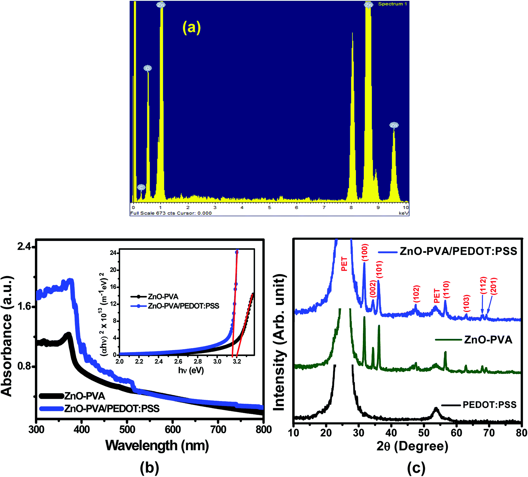
The surface topography of PEDOT:PSS films were carried out (scan area 1 mm × 1 mm) before and after spin coating of ZnO–PVA nanocomposite by atomic force microscopy (AFM) in tapping mode using phosphorous doped silicon cantilever. Fig. 1(a) and (b) show the plane view AFM micrographs of pristine PEDOT:PSS films and ZnO–PVA nanocomposite/PEDOT:PSS heterostructure sample formed on flexible Al coated PET substrates. The surface roughness of the nanocomposite films was determined from AFM topography in 1 mm × 1 mm area. The RMS surface roughness for pristine PEDOT:PSS films and ZnO–PVA/PEDOT:PSS films were estimated to be 33 nm and 85.3 nm, respectively. The higher surface roughness for ZnO–PVA/PEDOT:PSS film is attributed to the presence of ZnO–PVA nanocomposite. The micrograph clearly indicates the formation of ZnO nanoparticles (NPs) uniformly distributed in large area. The particle size distribution is plotted at the inset of Fig. 1(b). From the histogram, the diameter of the nanoparticles variation can be estimated as 15–60 nm and the average diameter of the nanoparticles is found to be 35 nm. The average nanoparticle density has been estimated from 1 μm × 1 μm surface area and found to be ∼3 × 10¹³ NPs per m2. Fig. 1(c) represents the typical SEM micrograph of ZnO nanosheets embedded in PVA matrix. It has been observed that ZnO NPs forms nanosheets-like structure inside the PVA matrix. The magnified SEM image of the ZnO nanosheets embedded in PVA matrix as depicted in the inset of Fig. 1(c). It is clearly seen that the SEM micrograph revealed the formation of ZnO nanosheets of thickness 20–40 nm with several micron lengths. Fig. 1(d) shows a cross-sectional view of the grown switching memory structure on flexible Al coated PET substrates. The FESEM micrograph clearly indicates ZnO–PVA nanocomposite, PEDOT:PSS film and Al electrode with sharp interfaces. The thicknesses of the ZnO–PVA nanocomposite and PEDOT:PSS films are estimated to be 100 nm and 180 nm, respectively. Fig. 2(a) represents the typical energy dispersive X-ray (EDX) spectrum of ZnO–PVA nanocomposites. The EDX spectrum confirms the presence of Zn and O elements in ZnO–PVA nanocomposites. The elemental analysis reveals the formation of stoichiometrically pure ZnO in PVA matrix. The additional elements Zn, O and C arise from carbon coated copper grids and PVA polymer.
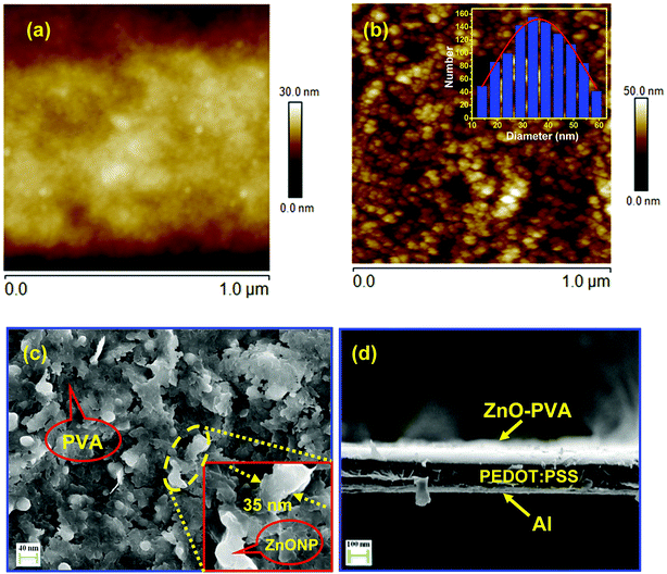 |
| | Fig. 1 Plane view of AFM surface topography of (a) pristine PEDOT:PSS films. (b) ZnO–PVA nanocomposite/PEDOT:PSS heterostructure deposited on flexible Al coated PET substrates. The particle size distribution is plotted at the inset. (c) Plane view SEM image of ZnO–PVA nanocomposite deposited on the surface of PEDOT:PSS films. (d) The cross sectional SEM image of ZnO–PVA nanocomposite/PEDOT:PSS/Al heterostructure sample. | |
 |
| | Fig. 2 (a) Energy dispersive X-ray spectrum (EDX) of ZnO nanoparticles embedded in PVA matrix. (b) UV-visible absorption spectra of ZnO–PVA nanocomposite films and ZnO–PVA nanocomposite/PEDOT:PSS heterostructure films. (αhν)2 vs. hν plot for ZnO–PVA nanocomposite and ZnO–PVA/PEDOT:PSS heterostructure (inset). (c) X-ray diffraction spectra of PEDOT:PSS, ZnO–PVA nanocomposite and ZnO–PVA nanocomposite/PEDOT:PSS heterostructure grown on PET substrates. | |
3.2 Optical characterization
Fig. 2(b) shows the UV-visible absorption spectra of ZnO–PVA nanocomposite films with and without attachment of PEDOT:PSS in the range of 300–800 nm. The optical band gap (Eg) of ZnO–PVA nanocomposite has been calculated using Tauc's formula.36where α is the absorption coefficient, hν is the incident photon energy and A is a constant. Inset of Fig. 2(b) represents (αhν)2 vs. hν plot for both samples. The optical band gap of ZnO–PVA nanocomposite and absorption edge of ZnO–PVA nanocomposite/PEDOT:PSS have been calculated by extrapolation at the linear region of (αhν)2 vs. hν plot to the energy axis. The pristine ZnO–PVA nanocomposite shows strong absorption in the UV region of wavelength threshold at 387 nm, corresponding to the energy band gap of 3.2 eV. Interestingly, the absorption edge has been slightly shifted to higher wavelength for ZnO–PVA nanocomposite deposited on PEDOT:PSS films (∼3.15 eV), which is attributed to the strengthened photoabsorption in visible region. Moreover, the additional peak at 503 nm has been observed, which is attributed to the absorption edge of ZnO–PVA nanocomposite/PEDOT:PSS.37 Fig. 2(c) shows the XRD spectra of the PEDOT:PSS film, ZnO–PVA nanocomposite films and ZnO–PVA nanocomposite/PEDOT:PSS heterostructure films deposited on Al coated flexible PET substrates. The XRD result clearly indicates that both ZnO–PVA nanocomposites and ZnO–PVA nanocomposite/PEDOT:PSS are highly crystalline. The strongest diffraction peaks observed at 2θ = 31.72°, 34.40°, 36.21°, 47.49°, 56.52°, 62.80°, 67.83°, and 68.97° corresponding to the lattice planes (100), (002), (101), (102), (110), (103), (112), and (201) respectively, are attributed to the hexagonal wurtzite structure of ZnO. The data is in well agreement with the JCPDS card number 36-1451.38 Interestingly, ZnO–PVA nanocomposites/PEDOT:PSS exhibits the same diffraction patterns with ZnO–PVA nanocomposites, and the additional diffraction peaks at 26° and 52.9° have been observed due to the diffraction from PET substrate.39 However, no diffraction peak can be observed for the pure PEDOT:PSS film except two diffraction peaks at 26° and 52.9° due to the diffraction from PET substrate,39 demonstrating its poor crystalline structure.
3.3 Electrical characterization
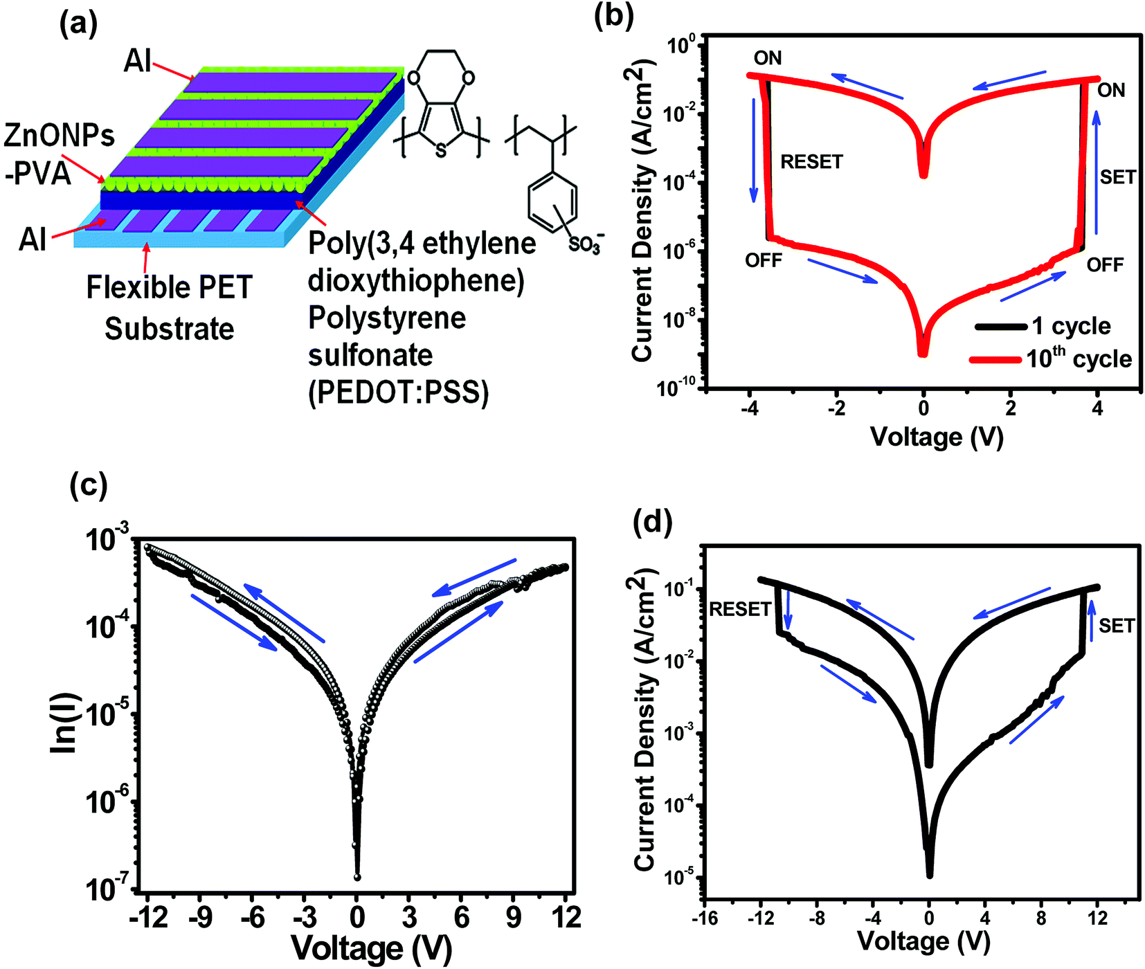
To study the resistive switching characteristics of ZnO–PVA nanocomposites [concentration ratio (ZnO:PVA) of 10:1]/conducting polymer heterostructure, the following three samples have been fabricated. The samples are (i) Al/PEDOT:PSS/Al/flexible PET substrate (denoted as S1), (ii) Al/ZnO–PVA/Al/flexible PET substrate (denoted as S2) and (iii) Al/ZnO–PVA/PEDOT:PSS/Al/flexible PET substrate (denoted as S3). In electrical measurements, Al top electrodes (TE) were connected to negative (‘−’) and Al bottom electrodes (BE) were connected to positive (‘+’) terminal to the source meter. Fig. 3(a) shows the schematic diagram of the S3 memory device and molecular structure of PEDOT:PSS film. Fig. 3(b) shows the current–voltage (I–V) switching characteristics of the S3 device. The external electrical stimulation is supplied to the device in the form of an applied voltage in a sequence of 0 V → +4 V → 0 V → −4 V → 0 V, with a current compliance of 5.1 × 10⁻² A to prevent the permanent dielectric breakdown of the device. The high-conductivity state (ON-state) was achieved by applying a forward voltage sweep on the device. With increasing positive voltage, the current starts increasing and jumps suddenly at +3.6 V, indicating the switching of the device from low conductivity state (OFF-state) to high-conductivity state (ON-state). This switching process from OFF state to ON state is referred to as the “writing” process, and which is known as the SET process. The ON state will remain in that state and will not return to the OFF state even after turning off the power supply (read process). The high conducting state (ON state) process is maintained from +4 V to −4 V, while reverse sweeping. Subsequently, the ON state switches to a low conducting state (OFF state) at a voltage of −3.6 V, as can be seen in the reverse bias voltage. This transition from ON state to OFF state is equivalent to the ‘erasing’ process in a digital memory cell,40 which is also known as the RESET process. The low conductivity state (OFF-state) of the device can be read and reprogrammed to the high-conductivity state (ON-state) in the subsequent positive sweep, as a result, completing the “write → read → erase → read → rewrite” cycle for a non-volatile rewritable memory device.41 It is observed that, the existence of two conducting states, viz., low conductivity state (OFF state) and high conductivity state (ON state), exhibiting bistable behaviour. The state of the device was maintained even after removal of the applied bias, indicating the non-volatile memory. It is also seen that, the reversible resistance switching between low conductivity state (OFF state) and high conductivity state (ON state) promises to be used in the rewritable data storage system. Hence, non-volatile bistable memory was demonstrated. Such write or erase processes have been investigated cyclically for 10 times, and no significant changes were observed in the SET and RESET voltage. The ratio (ION/IOFF) of the current achieved between the ON and OFF states is about 3 × 10⁵ in magnitude at a reading voltage of 1 V as shown in Fig. 3(b).
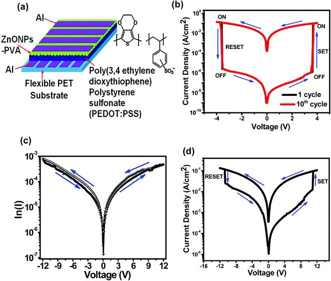 |
| | Fig. 3 (a) Schematic diagram of the S3 memory device and molecular structure of PEDOT:PSS films. Current–voltage (I–V) switching characteristics of the (b) S3 memory device, (c) S1 device and (d) S2 device. | |
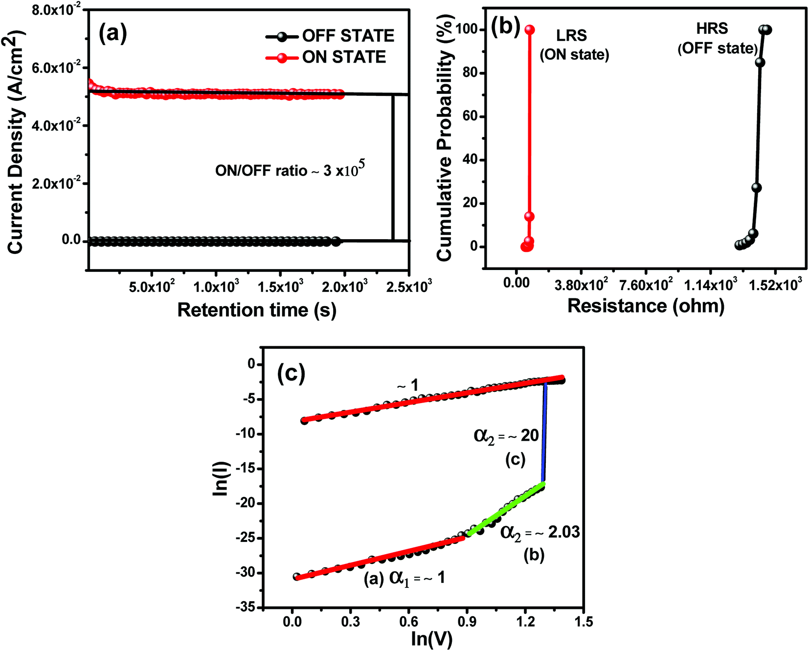
For comparison, the two samples S1 and S2 have been fabricated and measured. The electrical performances were inferior as compared to the S3 device, as shown in Fig. 3(c) and (d). It is observed that, the S1 device has no resistivity switching even at a higher operating voltage as shown in Fig. 3(c). In Fig. 3(d), the S2 device shows resistivity switching behaviour at a high operating voltage. But, the performance of the S3 device is significantly improved over the S2 device. The enhancement of the S3 device in resistivity switching behaviour is due to the presence of hole transporting PEDOT:PSS polymer with an efficient hole transport from ZnO to PEDOT:PSS, resulting in higher ‘ON state/OFF state’ current ratio, as shown in Fig. 3(b). Earlier studies have reported that multilevel conductance behaviour is revealed in the organic based memory devices,42,43 particularly, the devices utilizing metal/metal oxide nanocomposite as active materials. However, it is suggested from Fig. 3(b) that our S3 device did not show such behaviour since the currents at both ON and OFF state are rather constant. In practical applications, stability of the device performance is one of the most important characteristics of a memory device. The retention characteristics of the S3 device were analyzed for checking the durability. Fig. 4(a) shows the data-retention characteristics of the ON-state and the OFF-state currents as functions of time at room temperature. Firstly, the OFF state current measurement was carried out at 1 V. After that a pulsed positive bias (voltage 4 V and time 2 μs) was applied to change the device to ON state followed by the ON current measurement at a voltage of 1 V. It is seen that, there was no remarkable degradation of the device in both the ON state and OFF states after 32 minutes continuous operation which manifested excellent stability of the device. Furthermore, there is no noticeable degradation in S3 device performance even after 2 weeks after fabrication. The current values of both the ON states and OFF states are 5.1 × 10⁻² and 1.7 × 10⁻⁷A, respectively, and the ‘ON state/OFF state’ ratio is maintained at 3 × 10⁵, as shown in Fig. 4(a). The excellent stability and retention performances of this device verify the reliability of this sample and demonstrate their potential for application in non-volatile bistable memory device. Moreover, the resistances of OFF state and ON state in terms of the cumulative distribution were examined. Fig. 4(b) shows the cumulative probability of switching resistance of the S3 device. The resistance values measured at a read voltage of 1 V is plotted as ON state and OFF state. The distribution of ON state is quite narrow for the device, while the distribution of OFF state is, relatively, broader. The average values of ON state and OFF state are found to be 9 Ω and 1.4 kΩ, respectively, with a high resistance ratio (ON state/OFF state) of more than 3 × 10⁵. The presented S3 device provides an interesting candidate for high performance non-volatile flexible memory devices.
 |
| | Fig. 4 (a) Retention time measurements of the S3 organic bistable device (OBD) with a read voltage of 1 V. (b) Cumulative probability of S3 memory devices. (c) Linear fitting of the S3 memory device for the I–V curve on a log–log scale showing the SCLC mechanism. | |
3.4 Conduction mechanism
To clarify the conduction mechanism of the S3 memory device, the I–V characteristics were re-plotted in a log–log scale as shown in Fig. 4(c). From this plot, it is clearly seen that, the I–V characteristics in OFF-state (low conductivity state) consist of three regions, namely, (a) ohmic region (I ∝ V) with a slope of α1 ∼ 1 at low voltages, (b) Child's square law region (I ∝ V) with a slope of α2 ∼ 2.03 at higher voltages, and (c) steep increase in current region (I ∝ Vm) with a slope of ∼20. Where V is the applied voltages between the two electrodes and m is a positive number. This kind of I–V behavior is in good agreement with typical trap-controlled space charge limited conduction (SCLC) mechanism.44 Whereas, the ON-state (high conductivity state) exhibits ohmic conduction behavior with a slope of ∼1, which is attributed to the formation of conductive path between the top electrode (TE) and bottom electrode (BE) in the S3 device during the SET process.
Carrier transport in the resistive switching memory device based on ZnO-polymer composites had been explained mostly by SCLC45,46 and Fowler–Nordheim (FN) tunneling.47 Kim et al.45 showed that the main conduction in Al/ZnO–PS composites/ITO followed SCLC by fitting the I–V curves. However, the conduction mechanism in the cases of Al/ZnO–PMMA composites/ITO were unclear because it was just predicted as charge trapping without exact fitting of the log–log plot of the I–V curves.11 The conduction mechanism largely depends on the structure and electrical properties of the polymer matrix. It is note-worthy that compared with the Al/ZnO–polymer/ITO device, our S3 device exhibits bipolar memory behavior. In addition, it has been previously reported that the heterojunctions and interface play important roles in the bipolar resistance switching memory.48,49
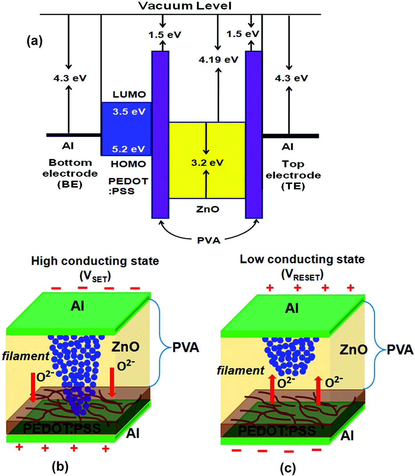
Based on the analysis above, it can be explained the conduction mechanism based on the formation and rupture of conduction filaments. In S3 device structure, the resistive switching is originated from the formation and rupture of the conduction filaments between two electrodes due to the migration of oxygen ions. The schematic diagrams of energy level corresponding to the operating mechanism for the S3 memory device as shown in Fig. 5(a). The lowest unoccupied molecular orbital (LUMO) and highest occupied molecular orbital (HOMO) levels for the PEDOT:PSS layer are 3.5 eV and 5.2 eV, respectively.50 The reported values of work function for Al and ZnO have been utilized in the proposed model,51,52 while the electron affinity of the PVA barrier is assumed to be ∼1.5 eV, similar to that of a non-conducting polymer. As shown in Fig. 5(b), when the positive voltage is applied to the device, some oxygen atoms are pulled out of the ZnO lattice, generating oxygen vacancies. These oxygen ions, act as p-type dopant, will move toward the PEDOT:PSS film and leave behind the tiny conducting filaments of oxygen vacancies in the ZnO–PVA composite layer. As a result, reducing the thickness of the depletion layer between p-type PEDOT:PSS and n-type ZnO. Subsequently, when the positive voltage reaches to SET voltage (VSET) of ∼+3.6 V, those tiny conducting filaments gather speedily to form more conducting and stronger filaments leading to breakout the depletion layer of the ZnO/PEDOT:PSS interface and the conductive pathways connect from top electrode (TE) to bottom electrode (BE), which will convert to the ON state of the device, which is known as the SET process (read process). Then the charges can flow through the conductive filaments and sustain the device in an ON state (high conducting state). Conversely, as shown in Fig. 5(c), the oxygen ions in the PEDOT:PSS film might be pushed forward to ZnO composites under a negative voltage. When the conductive filaments path consisted of oxygen vacancies are neutralized by sufficient oxygen ions, conduct filaments rupture at the ZnO composites/PEDOT:PSS interface and device switches to the OFF state (low conducting state), which is also known as the RESET process (erase process). The PEDOT:PSS, acting as an oxygen ions supplier, can switch the device back to OFF state more efficiently and completely. In brief, the PEDOT:PSS in S3 device attributing to oxygen ions reservoir in SET process and acting as an oxygen ions supplier in RESET process. Additionally, PEDOT:PSS is a hole conducting polymer with high electrical conductivity up to 200 S cm−1 and often used in organic memory device.53 The addition of a thin PEDOT:PSS layer with S2 device, improves the performance of oxygen ions (holes) transportation toward the bottom electrode (BE) and protect back oxygen vacancies (electrons) migrate toward the bottom electrode (BE) from ZnO–PVA composite which may reduces the leakage current. Consequently, increased the ‘ON state/OFF state’ current ratio of 7.9 × 10³ times. Hence, S3 device has superior resistive switching behavior compared to S2 device.
 |
| | Fig. 5 Schematic diagrams of energy level corresponding to the operating mechanism for the S3 memory device. Schematic diagrams of the electronic structures corresponding to the operating mechanisms for S3 memory device with the (b) high conducting state (SET state) and the (c) low conducting state (RESET state). | |
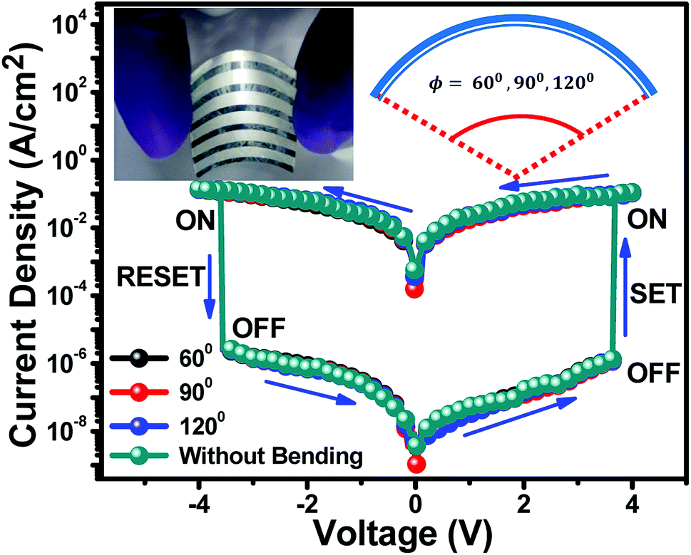
3.5 Flexibility study
In this present study, it has been demonstrated that the potential use of S3 non-volatile bistable memory device in flexible electronic applications. Fig. 6 represents the I–V switching characteristics of non-volatile bistable memory device without and with bending of angle 60°, 90° and 120°. The photograph of organic bistable memory device with bending is presented at the inset of Fig. 6. Interestingly, the I–V switching characteristics remained unchanged even after bending the device from 60–120° angles, which is attractive for flexible electronic applications.
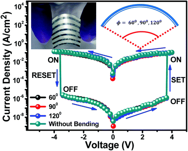 |
| | Fig. 6 Current–voltage (I–V) switching characteristic of the S3 memory device. I–V switching characteristic were recorded at 180° (without bending), 60°, 90° and 120° bending angles of the substrates. Photograph demonstrates the flexibility of a typical S3 memory device (inset). | |
4. Conclusions
In conclusion, we have demonstrated the flexible non-volatile bistable resistive switching memory device using colloidal ZnO–PVA nanocomposites and PEDOT:PSS film deposited on Al coated flexible PET substrate. The surface roughness of the pristine PEDOT:PSS and ZnO–PVA/PEDOT:PSS was determined from AFM topography in 1 mm × 1 mm area. The RMS surface roughness for pristine PEDOT:PSS films and ZnO–PVA/PEDOT:PSS films were estimated to be 33 nm and 85.3 nm, respectively. The higher surface roughness for ZnO–PVA/PEDOT:PSS film which was due to the presence of ZnO–PVA nanocomposite. SEM micrograph clearly revealed the formation ZnO nanosheets of thickness 20–40 nm with several micron lengths. It was observed that, ZnO NPs forms nanosheets-like structure inside the PVA matrix. The EDX spectrum analysis confirms the presence of Zn and O elements in ZnO–PVA nanocomposites. The elemental analysis reveals the formation of stoichiometrically pure ZnO in PVA matrix. The additional elements Zn, O and C arise from carbon coated copper grids and PVA polymer. I–V characteristic of the S3 device exhibited flexible non-volatile bistable resistive switching characteristics. The performance of the S3 device is considerably improved over control S1 and S2 devices, this is due to the presence of PEDOT:PSS polymer. This PEDOT:PSS improves the performance of oxygen ions (holes) transportation toward bottom electrode (BE) and protect back oxygen vacancies (electrons) transfer toward BE from ZnO–PVA composites which may reduces the leakage current. The existence of two conducting states, namely, OFF state and ON state, exhibiting bistable behaviour of S3 device. The state (ON state or OFF state) of the device was maintained even after turn off power supply, demonstrating the non-volatile memory. The data of S3 device can be written and erased by applying a positive and negative bias of +3.6 V and −3.6 V, respectively. The ratio (ION/IOFF) of the current occurred between the ON and OFF states is about 3 × 10⁵ in magnitude at a reading voltage of 1 V. The retention characteristics of the S3 device were analyzed for checking the durability, it was seen that, there was no significant degradation of the device in both the ON and the OFF states after 32 minutes continuous operation which demonstrated that the device was stable. The excellent stability and good retention performances of S3 device confirm the reliability of this device and exhibit their potential for application in non-volatile bistable memory device.
Interestingly, the results clearly show that there was no detectable change in resistive switching even after bending the S3 memory device with angles 60°, 90° and 120°, making it compatible with flexible electronics. Our device has sufficient potential to be used as a non-volatile resistive switching memory device in various flexible electronic devices.
Conflicts of interest
There is no conflicts to declare.
Acknowledgements
This research work was funded by UGC-BSR Research Start-Up-Grant, Sanction No. F.30-412/2018(BSR) dated 23/03/2018, Government of India. Author acknowledges the Centre for Research in Nanoscience and Nanotechnology (CRNN) of University of Calcutta for SEM measurement.
References
- S. Coe, W.-K. Woo, M. Bawendi and V. Bulovic, Electroluminescence from single monolayers of nanocrystals in molecular organic devices, Nature, 2002, 420, 800–803 CrossRef PubMed.
- J. H. Jung, J. Y. Jin, I. Lee, T. W. Kim, H. G. Roh and Y. H. Kim, Memory effect of ZnO nanocrystals embedded in an insulating polyimide layer, Appl. Phys. Lett., 2006, 88, 112107 CrossRef.
- J. H. Jung, J. H. Kim, T. W. Kim, C. S. Yoon, Y. H. Kim and S. Jin, Nonvolatile memory cell effect in multilayered Ni1-xFex self-assembled nanoparticle arrays in polyimide, Appl. Phys. Lett., 2006, 89, 022112 CrossRef.
- C.-J. Sun, Y. Wu, Z. Xu, B. Hu, J. Bai, J.-P. Wang and J. Shen, Enhancement of quantum efficiency of organic light emitting devices by doping magnetic nanoparticles, Appl. Phys. Lett., 2007, 90, 232110 CrossRef.
- S. Kolliopoulou, P. Dimitrakis, P. Normand, H.-L. Zhang, N. Cant, S. D. Evans, S. Paul, C. Pearson, A. Molloy, M. C. Petty and D. Tsoukalas, Hybrid silicon–organic nanoparticle memory device, J. Appl. Phys., 2003, 94, 5234 CrossRef.
- C. Li, W. Fan, B. Lei, D. Zhang, S. Han, T. Tang, X. Liu, Z. Liu, S. Asano, M. Meyyappan, J. Han and C. Zhou, Multilevel memory based on molecular devices, Appl. Phys. Lett., 2004, 84, 1949 CrossRef.
- W. L. Leong, P. S. Lee, S. G. Mhaisklkar, T. P. Chen and A. Dodablapur, Charging phenomena in pentacene-gold nanoparticle memory device, Appl. Phys. Lett., 2007, 90, 042906 CrossRef.
- S. Sahu, S. K. Majee and A. J. Pai, Layer-by-layer assembly of capped CdSe nanoparticles: Electrical bistability and memory phenomenon, Appl. Phys. Lett., 2007, 91, 143108 CrossRef.
- A. W. Tang, F. Teng, Y. B. Hou, Y. S. Wang, F. R. Tan, S. C. Qu and Z. G. Wang, Optical properties and electrical bistability of CdS nanoparticles synthesized in dodecanethiol, Appl. Phys. Lett., 2010, 96, 163112 CrossRef.
- C. H. V. V. Ramana, M. K. Moodely, V. Kannan, A. Maity, J. Jayaramudu and W. Clarke, Fabrication of stable low voltage organic bistable memory device, Sens. Actuators, B, 2012, 161, 684–688 CrossRef.
- D. T. Thanh, T. T. Viet, H. Koichi, O. Hiromasa, D. Mott, S. Maenosono and H. Murata, High-performance non-volatile write-once-read many-times memory devices with ZnO nanoparticles embedded in polymethylmethacrylate, Appl. Phys. Lett., 2011, 99, 233303 CrossRef.
- X. F. Duan and C. M. Lieber, General Synthesis of Compound Semiconductor Nanowires, Adv. Mater., 2000, 12, 298 CrossRef.
- R. J. Warburton, C. Schaflein, D. Haft, F. Bickel, A. Lorke, K. Karrai, J. M. Garcia, W. Schoenfeld and P. M. Petroff, Optical emission from a charge-tunable quantum ring, Nature, 2000, 405, 926–929 CrossRef PubMed.
- B. H. Kind, H. Yan, B. Messer, M. Law and P. Yang, Nanowire Ultraviolet Photodetectors and Optical Switches, Adv. Mater., 2002, 14, 158 CrossRef.
- X. Li, Y. Wu, D. Steel, D. Gammon, T. H. Stievater, D. S. Katzer, D. Park, C. Piermarocchi and L. J. Sham, An all-optical quantum gate in a semiconductor quantum dot, Science, 2003, 301, 809 CrossRef PubMed.
- N. J. Craig, J. M. Taylor, E. A. Lester, C. M. Marcus, M. P. Hanson and A. C. Gossard, Tunable Non-local Spin Control in a Coupled Quantum Dot System, Science, 2004, 304, 565 CrossRef PubMed.
- J. H. Kim, J. Y. Jin, J. H. Jung, I. Lee, T. W. Kim, S. K. Lim, C. S. Yoon and Y.-H. Kim, Formation and electrical properties of Ni1−xFex nanocrystals embedded in a polyimide layers for applications as nonvolatile flash memories, Appl. Phys. Lett., 2005, 86, 032904 CrossRef.
- F. Li, D.-I. Son, J.-H. Ham, G.-J. Kim, J. H. Jung and T. W. Kim, Memory effect of non-volatile bistable devices based on CdSe/ZnS nanoparticles sandwiched between C60 layers, Appl. Phys. Lett., 2007, 91, 162109 CrossRef.
- T. Y. Chang, Y. W. Cheng and P. T. Lee, Electrical characteristics of an organic bistable device using an Al/Alq3 nanostructured MoO3/Alq3/p+-Si structure, Appl. Phys. Lett., 2009, 96, 043309 CrossRef.
- D. Wang, B. Kowalczyk, I. Lagzi and B. A. Grzybowski, Bistability and Hysteresis During Aggregation of Charged Nanoparticles, J. Phys. Chem. Lett., 2010, 1, 1459 CrossRef.
- Y. S. Lai, C. H. Tu and D. L. Kwong, Bistable resistance switching of poly(N-vinylcarbazole) films for nonvolatile memory applications, Appl. Phys. Lett., 2005, 87, 122101 CrossRef.
- S. H. Kim, K. S. Yook, J. Y. Lee and J. Jang, Organic light emitting bistable memory device with high on/off ratio and low driving voltage, Appl. Phys. Lett., 2008, 93, 053306 CrossRef.
- S. Song, B. Cho, T. W. Kim, Y. Ji, M. Jo, G. Wang, M. Choe, Y. H. Kahng, H. Hwang and T. Lee, Three-Dimensional Integration of Organic Resistive Memory Devices, Adv. Mater., 2010, 22, 5048–5052 CrossRef PubMed.
- H. T. Lin, Z. Pei and Y. J. Chan, Carrier Transport Mechanism in a Nanoparticle-Incorporated Organic Bistable Memory Device, IEEE Electron Device Lett., 2007, 28, 569 CrossRef.
- R. N. Koteeswara, M. Devika and C. W. Tu, Vertically aligned ZnO nanorods on flexible substrates for multifunctional device applications: easy and cost-effective route, Mater. Lett., 2014, 120, 662–664 Search PubMed.
- A. Kathalingam, H.-S. Kim, S.-D. Kim, H.-M. Park and H.-C. Park, Unipolar resistive switching of solution synthesized ZnO nanorod with self-rectifying and negative differential resistance effects, Mater. Lett., 2015, 142, 238–241 CrossRef.
- S. Paul, P. G. Harris, C. Pal, A. K. Sharma and A. K. Ray, Low cost zinc oxide for memristors with high on-off ratios, Mater. Lett., 2014, 130, 40–42 CrossRef.
- B. Sun, W. Zhao, L. Wei, H. Li and P. Chen, Enhanced resistive switching effect upon illumination in self-assembled NiWO4 nano-nests, Chem. Commun., 2014, 50, 13142–13145 RSC.
- B. Sun and C. M. Li, Light-controlled resistive switching memory of multiferroic BiMnO3 nanowire arrays, Phys. Chem. Chem. Phys., 2015, 17, 6718–6721 RSC.
- W. Y. Chang, Y. C. Lai, T. B. Wu, S. F. Wang, F. Chen and M. J. Tsai, Unipolar resistive switching characteristics of ZnO thin films for nonvolatile memory applications, Appl. Phys. Lett., 2008, 92, 022110 CrossRef.
- C. Chen, F. Pan, Z. S. Wang, J. Yang and F. Zeng, Bipolar resistive switching with self-rectifying effects in Al/ZnO/Si structure, J. Appl. Phys., 2012, 111, 013702 CrossRef.
- N. Xu, L. F. Liu, X. Sun, X. Y. Liu, D. D. Han, Y. Wang, R. Q. Han, J. F. Kang and B. Yu, Characteristics
and mechanism of conduction/set process in TiN/ZnO/PtTiN/ZnO/Pt resistance switching random-access memories, Appl. Phys. Lett., 2008, 92, 232112 CrossRef.
- W. Y. Chang, H. W. Huang, W. T. Wang, C. H. Hou, Y. L. Chueh and J. H. He, High Uniformity of Resistive Switching Characteristics in a Cr/ZnO/Pt Device, J. Electrochem. Soc., 2012, 159, G29–G32 CrossRef.
- J. Lee, E. M. Bourim, W. Lee, J. Park, M. Jo, S. Jung, J. Shin and H. Hwang, Effect of ZrOx/HfOxZrOx/HfOx bilayer structure on switching uniformity and reliability in nonvolatile memory applications, Appl. Phys. Lett., 2010, 97, 172105 CrossRef.
- T. Majumder, J. J. L. Hmar, K. Debnath, N. Gogurla, J. N. Roy, S. K. Ray and S. P. Mondal, Photoelectrochemical and photosensing behaviors of hydrothermally grown ZnO nanorods, J. Appl. Phys., 2014, 116, 034311 CrossRef.
- J. I. Pankove, Optical Processes in Semiconductors, Prentice-Hall, Englewood Cliffs, NJ, 1971 Search PubMed.
- T. Abdiryim, A. Ali, R. Jamal, Y. Osman and Y. Zhang, A facile solid-state heating method for preparation of poly(3,4- ethelenedioxythiophene)/ZnO nanocomposite and photocatalytic activity, Nanoscale Res. Lett., 2014, 9, 89 CrossRef PubMed.
- V. P. Dinesh, P. Biji, A. Ashok, S. K. Dhara, M. Kamaruddin, A. K. Tyagi and B. Raj, Plasmon-Mediated Highly Enhanced Photocatalytic Degradation of Industrial Textile Effluent Dyes using Hybrid ZnO@Ag Core-shell Nanorods, RSC Adv., 2014, 4, 58930–58940 RSC.
- W. L. Ong, Q. X. Low, W. Huang, J. A. V. Kan and G. W. Ho, Patterned growth of vertically aligned ZnO nanorods on a flexible platform for feasible transparent and conformable electronics applications, J. Mater. Chem., 2012, 22, 8518–8524 RSC.
- L. P. Ma, S. M. Pyo, J. Y. Ouyang, Q. Y. Xu and Y. Yang, Nonvolatile electrical bistability of organic/metal-nanocluster/organic system, Appl. Phys. Lett., 2003, 82, 1419 CrossRef.
- G. L. Li, G. Liu, M. Li, D. Wan, K. G. Neoh and E. T. Kang, Organo- and Water-Dispersible Graphene Oxide-Polymer Nanosheets for Organic Electronic Memory and Gold Nanocomposites, J. Phys. Chem. C, 2010, 114, 12742–12748 Search PubMed.
- M. Lauters, B. McCarthy, D. Sarid and G. E. Jabbour, Nonvolatile multilevel conductance and memory effects in organic thin films, Appl. Phys. Lett., 2005, 87, 231105 CrossRef.
- V. S. Reddy, S. Karak and A. Dhar, Multilevel conductance switching in organic memory devices based on AlQ3 and Al/Al2O3 core-shell nanoparticles, Appl. Phys. Lett., 2009, 94, 173304 CrossRef.
- M. Lampert, Simplified Theory of Space-Charge-Limited Currents in an Insulator with Traps, Phys. Rev., 1956, 103(6), 1648–1656 CrossRef.
- D. Y. Yun, J. K. Kwak, J. H. Jung, T. W. Kim and D. I. Son, Electrical bistabilities and carrier transport mechanisms of write-once read- many-times memory devices fabricated utilizing ZnO nanoparticles embedded in a polystyrene layer, Appl. Phys. Lett., 2009, 95, 143301 CrossRef.
- D. I. Son, D. H. Park, W. K. Choi, S. H. Cho, W. T. Kim and T. W. Kim, Carrier transport in flexible organic bistable devices of ZnO nanoparticles embedded in an insulating poly(methyl methacrylate) polymer layer, Nanotechnology, 2009, 20, 195203 CrossRef PubMed.
- D. I. Son, C. H. You, W. T. Kim, J. H. Jung and T. W. Kim, Electrical bistabilities and memory mechanisms of organic bistable devices based on colloidal ZnO quantum dot polymethylmethacrylate polymer nanocomposites, Appl. Phys. Lett., 2009, 95, 132103 CrossRef.
- D. Varandani, B. Singh, B. R. Mehta, M. Singh, V. N. Singh and D. Gupta, Resistive switching mechanism in delafossite-transition metal oxide (CuInO2–CuO) bilayer structure, J. Appl. Phys., 2010, 107, 103703 CrossRef.
- H. J. Zhang, X. P. Zhang, J. P. Shi, H. F. Tian and Y. G. Zhao, Effect of oxygen content and superconductivity on the nonvolatile resistive switching in YBa2Cu3O6+x doped SrTiO3 heterojunctions, Appl. Phys. Lett., 2009, 94, 092111 CrossRef.
- K. W. Lee1, K. M. Kim, J. Lee, R. Amin, B. Kim, S. K. Park, S. K. Lee, S. H. Park and H. J. Kim, A two-dimensional DNA lattice implanted polymer solar cell, Nanotechnology, 2011, 22, 375202 CrossRef PubMed.
- S. P. Mondal, V. S. Reddy, S. Das, A. Dhar and S. K. Ray, Memory effect in a junction-like CdS nanocomposite/conducting polymer poly[2-methoxy-5-(2-ethylhexyloxy)- 1,4-phenylene-vinylene] heterostructure, Nanotechnology, 2008, 19, 215306 CrossRef PubMed.
- N. Zhang, W. Tang, P. Wang, X. Zhang and Z. Zhao, In situ enhancement of NBE emission of Au–ZnO composite nanowires by SPR, CrystEngComm, 2013, 15, 3301–3304 RSC.
- J. J. L. Hmar, T. Majumder, J. N. Roy and S. P. Mondal, Electrical and photoelectrochemical characteristics of flexible CdS nanocomposite/conducting polymer heterojunction, Mater. Sci. Semicond. Process., 2015, 40, 145–151 CrossRef.
Footnote |
| † Electronic supplementary information (ESI) available: Current–voltage (I–V) resistive switching characteristics of S3 device at different concentration of ZnO in ZnO–PVA nanocomposites. See DOI: 10.1039/c8ra04582h |
|
| This journal is © The Royal Society of Chemistry 2018 |
Click here to see how this site uses Cookies. View our privacy policy here. 
 Open Access Article
 This Open Access Article is licensed under a Creative Commons Attribution-Non Commercial 3.0 Unported Licence
 *
*