DOI:
10.1039/C8RA04558E
(Paper)
RSC Adv., 2018,
8, 29089-29095
Low defects, large area and high stability of all-inorganic lead halide perovskite CsPbBr3 thin films with micron-grains via heat-spraying process for self-driven photodetector†
Received
28th May 2018
, Accepted 30th July 2018
First published on 15th August 2018
Abstract
All-inorganic lead halide perovskite CsPbBr3 has important applications in photoelectronic devices such as photodetectors, LEDs and photovoltaic devices. However, preparing high-quality CsPbBr3 thin films has proven to be challenging. In this study, we prepared all-inorganic lead halide perovskite CsPbBr3 thin films with micron-grains (MG-CsPbBr3-TF) via a heat-spraying process (HSP) using a CsPbBr3-saturated solution (CsPbBr3-SS), and the films exhibited large area, low defects and high stability. The grain size of MG-CsPbBr3-TF was about 1–5 microns. The micron-sized grains in MG-CsPbBr3-TF enabled the absorption cutoff edge to be extended from 537 to 545 nm. In addition, the presence of fewer boundaries in MG-CsPbBr3-TF reduced the defects in MG-CsPbBr3-TF (the blue shift of luminescence). The response wavelengths of a low-cost and self-driven (zero-biased) photodetector based on MG-CsPbBr3-TF were from 330 to 600 nm. CsPbBr3 thin films having a large area (10 cm × 10 cm) and micron-sized grains were also prepared by HSP and exhibited excellent stability (1944 h) in air (T = 298 K, 40% humidity). To the best of our knowledge, this is the first study of high-quality CsPbBr3 thin films prepared by HSP. The results are of great interest for both fundamental research and practical applications of CsPbBr3 in photodetectors, LEDs and photovoltaic devices.
1. Introduction
Lead halide perovskite (LHP) materials have become a research hotspot because of their novel physical and chemical properties.1–4 Recently, organic–inorganic LHP material-based thin film solar cells have demonstrated high power conversion efficiencies (PCEs) of more than 22%,5 competing with commercially available silicon solar cells. Thus, organic–inorganic LHP materials have attracted widespread attention. However, the stability of organic–inorganic LHP materials is not ideal. One of the drawbacks of organic–inorganic LHP materials is that the three-dimensional crystal structure can be easily destroyed by moisture in the air. In addition, these materials do not exhibit very good thermal stability above 180 °C. The use of all-inorganic perovskites is one of the ways to improve the stability of LHP. Compared to organic–inorganic LHP, all-inorganic LHP materials exhibit superior stability against moisture and temperature. An all-inorganic lead bromide perovskite (CsPbBr3) material functions equally well as the organic one, in particular for generating high open circuit voltages, which is an important feature of solar cells.6 In addition, CsPbBr3 is a direct band gap semiconductor, which meets most of the requirements for successful high-energy radiation detection of X-ray and gamma-ray radiation such as high attenuation, high resistivity, and significant photoconductivity response.7 Recently, CsPbBr3 was also applied as the emitting layer in LEDs8 and as a novel photocatalyst to convert CO2 into solar fuels in non-aqueous media.9 Therefore, CsPbBr3 is a very promising optoelectronic material for many applications.10–13
CsPbBr3 nanocrystals were currently synthesized by injecting the organic cesium precursor Cs-oleate into a ligand solvent (oleic acid/oleylamine/1-octadecene).14,15 The CsPbBr3 thin film with nano-grains (NG-CsPbBr3-TF) can be prepared by depositing CsPbBr3 nanocrystals. However, the CsPbBr3 thin film with micron-sized grains (MG-CsPbBr3-TF) has received less attention; nonetheless, it plays an important role in improving the performance of optoelectronic devices. Thus, CsPbBr3 thin films with micron-sized grains urgently need to be developed. In this study, CsPbBr3 thin films with micron-sized grains were formed from CsPbBr3-saturated solution (CsPbBr3-SS) by a heat-spraying process (HSP).
2. Experimental
2.1. Fabrication of CsPbBr3 thin film with micron-sized grains by heat-spraying method
Patterned FTO-coated glass with sheet resistance of 15 Ω sq−1 was coated with a TiO2 electronic collection layer (ECL) by spin-coating a TiO2 organic sol at 3000 rpm for 30 s, followed by drying at 450 °C for 120 min. Next, a CsPbBr3 thin film with micron-sized grains was prepared by spraying CsPbBr3-saturated solution on the TiO2 film at 200 °C. Finally, carbon electrodes were prepared by doctor-blade coating a conductive carbon paste on the CsPbBr3 layer using adhesive tapes as pattern and spaces, followed by drying at 80 °C for 10 min. The size of the FTO/TiO2/CsPbBr3/carbon electrode device was 1 cm2.
2.2. Fabrication of CsPbBr3 thin films with nano-sized grains by the heat-spraying method
2.2.1. Preparation of Cs-oleate. Cs2CO3 (0.30 g) was added into 1 mL oleic acid. 1-Octadecene (18 mL) was then added into the above-mentioned solution. The mixed solution was heated to 120 °C.
2.2.2. Preparation of CsPbBr3 nanocrystals. PbBr2 (0.10 g), 1 mL oleylamine, 5 mL 1-octadecene and 1 mL oleic acid were mixed. The mixed solution was heated to 200 °C. Then, 1 mL Cs-oleate was injected into the above solution. Finally, this solution was cooled down to room temperature naturally. CsPbBr3 nanocrystals were separated by centrifuging, and they were washed with butanol. The CsPbBr3 thin film with nano-grains was prepared by spraying CsPbBr3 nanocrystals in butanol on the TiO2 electronic transport layer at 200 °C.
2.3. Growth and characterizations of CsPbBr3 single crystals
In a typical procedure, a 50 mL round-bottom flask was filled with 0.122 g Cs2CO3 and 1.8 mL 47% HBr aqueous solution; 0.115 g PbBr2 was dissolved in this solution upon heating to 80 °C using an oil bath for 30 min, which resulted in the formation of a suspension. This suspension was transferred to one side of an H tube using a plastic dropper. The suspension in the side of the H tube was left for 24 h until the precipitate and supernatant were separated. One side of the H tube contained the suspension, whereas the other side contained a light yellow solution. The H tube was placed in the dark for two weeks. Yellow crystal particles were obtained in the side of the H tube having the pale yellow solution.
2.4. Characterizations
The nanostructures of our films were characterized by scanning electron microscopy (SEM, Nova Nano SEM 450). UV-Vis absorption spectra and diffuse reflectance spectra were obtained using a UV/vis/NIR spectrometer (PerkinElmer, lambda, 750S). The photocurrent–time performances of the devices were studied using an electrochemical workstation system (CHI760, Chenhua, and Shanghai) equipped with a solar simulator (IV5, PV Measurements, Inc., United States). The photocurrent–time with incident photon (wavelength) and frequency response was measured by an electrochemical workstation system (CHI760, Chenhua, and Shanghai) equipped with a quantum efficiency/spectral response (SR)/incident photon to current conversion efficiency (IPCE) measurement system (QEX10, PV Measurements, Inc., United States). External quantum efficiencies (EQE) were also measured by QEX10. The photocurrent–voltage performances of the devices were measured using a Keithley digital source meter (Keithley 2400, USA) equipped with a solar simulator (IV5, PV Measurements, Inc., USA).
3. Results and discussion
A schematic of the fabrication process of CsPbBr3 film by HSP is shown in Fig. 1. The detailed processes can be seen in the experimental section. In a typical procedure, CsPbBr3 suspension was obtained by the reaction between CsBr and PbBr2. Then, the suspension was transferred to one of the branches of H tube and left for 24 h until CsPbBr3 precipitate and supernatant (CsPbBr3-saturated solution) were separated. The CsPbBr3-saturated solution was collected in the other branch of the H tube by slowly tilting it. Consequently, one side of the H tube had the CsPbBr3 suspension, whereas the other had CsPbBr3-saturated solution. There are two advantages to the use of the H tube. First, the H tube can more effectively separate precipitate from the saturated solution. Second, CsPbBr3-saturated solution can be re-obtained by adding HBr solution by dissolution–precipitation equilibrium. The CsPbBr3-saturated solution can not only produce CsPbBr3 thin films with micron-sized grains by a heat-spraying process (HSP) but also grow single crystals, as shown in Fig. 1.
| Cs2CO3 + 2HBr = 2CsBr + CO2↑ + H2O, |
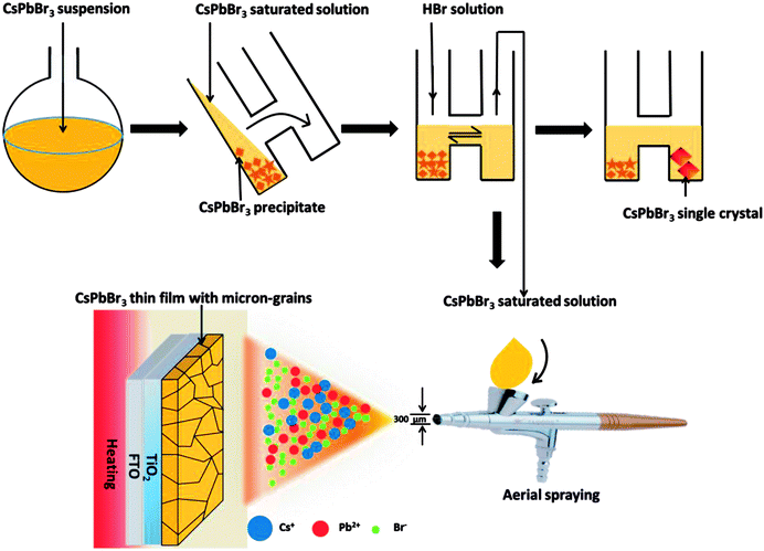 |
| | Fig. 1 Schematic of CsPbBr3 thin film prepared by heat-spraying process using CsPbBr3-saturated solution. | |
CsPbBr3 thin films can be prepared by spraying CsPbBr3-SS onto a heated FTO/TiO2-ECL substrate. The color of CsPbBr3 thin film is affected by the substrate (TiO2-ECL) temperature, as shown in Fig. 2a. The colour of the thin film prepared at 200 °C on TiO2-ECL is orange (Fig. 2a). UV-visible absorption spectra and diffuse reflectance spectra of the films prepared under different temperatures are measured. The film prepared at 200 °C on TiO2-ECL exhibits strong absorption from 250 to 510 nm, as shown in Fig. 2b. The absorbance of the film decreases sharply after 510 nm. The films prepared at 100 and 300 °C on TiO2-ECL exhibit strong absorptions from 250 to 400 nm. The UV-visible diffuse reflectances of the thin films are also measured, as shown in Fig. 2c. The reflection intensity of the film prepared at 200 °C on TiO2-ECL is significantly weaker from 250 nm to 510 nm, which corresponds to the strong UV-visible absorption from 250 to 510 nm. Meanwhile, the thin films prepared at 100 and 300 °C on TiO2-ECL exhibit strong reflectance in the visible range. This corresponds to weak UV-visible absorption from 250 to 510 nm. The above results indicate that it is impossible to form an orange CsPbBr3 thin film at 100 or 300 °C on TiO2-ECL. To prove that the orange thin film prepared at 200 °C on TiO2-ECL is CsPbBr3, the crystal structure of the film is studied. The X-ray diffraction (XRD) pattern is shown in Fig. 2d. A series of diffraction peaks are clearly observed. These diffraction peaks are consistent with the Joint Committee on Powder Diffraction Standards Cards (PDF#73-2463 for CsPbBr3), revealing that the thin film prepared at 200 °C on TiO2-ECLhas an orthorhombic crystal structure [Pmnb (62) space group, 4.597 × 9.72 × 16.81 Å, 90.0 × 90.0 × 90.0]. The diffraction peaks at 10.6, 14.2, 20.4, 25.6, 29.7, 36.6, and 50.3° are assigned to the (011), (012), (101), (103), (122), (040), and (145) planes of orthorhombic CsPbBr3, respectively. To obtain the bandgap of the CsPbBr3 thin film sprayed at 200 °C on TiO2-ECL, its diffuse reflectance spectrum is converted into a Kubelka–Munk spectrum.16,17 According to the Kubelka–Munk formula, F(R) = (1 − R)2/2R, where R represents the percentage of reflection. The relationship between incident photon energy (hν) and Eg can be expressed as the transformed Kubelka–Munk equation [F(R)hν]p = A(hν − Eg), where Eg is the bandgap energy, A is the absorption constant, h is the Planck's constant, ν is the frequency of the light (s−1) and P is the power index related to the optical absorption process. Theoretically, P is equal to 1/2 or 2 for an indirect or a direct allowed transition, respectively. According to literature, CsPbBr3 can be regarded as having direct allowed transition. Thus, Eg for the CsPbBr3 thin film is determined to be approximately 2.2 eV from the x-intercept of the linear part of [F(R)hν]2 plot, as shown in Fig. 2e. The CsPbBr3 film having a large area of 10 cm × 10 cm can also be prepared by CsPbBr3-SS-HSP, as shown in Fig. 2f.
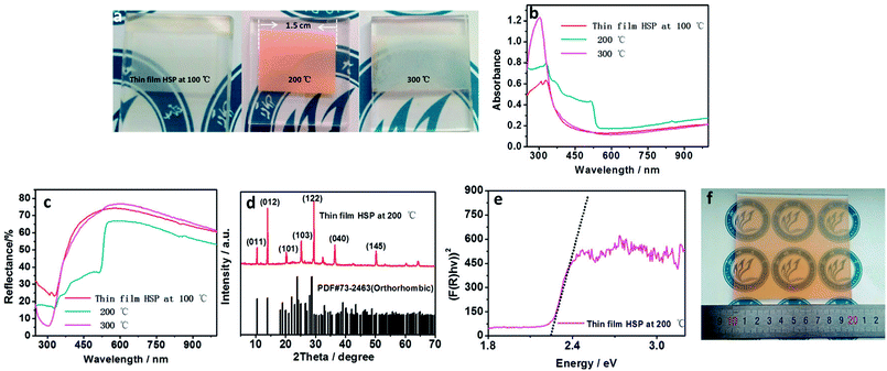 |
| | Fig. 2 (a) The colour of CsPbBr3 thin film prepared on a substrate at different temperatures. (b) UV-visible absorption spectra of CsPbBr3 thin film prepared on a substrate at different temperatures. (c) Diffuse reflectance spectra of CsPbBr3 thin film prepared on a substrate at different temperatures. (d) XRD profiles of CsPbBr3 thin film prepared on a substrate at 200 °C. (e) Transformed Kubelka–Munk spectrum of CsPbBr3 thin film prepared on a substrate at 200 °C. (f) Large area (10 cm × 10 cm) of CsPbBr3 film prepared by CsPbBr3-SS-HSP. | |
SEM (Fig. 3a) shows that the grains in CsPbBr3 thin film are in micron scale. The statistical distribution of grain size indicates that the grain size in MG-CsPbBr3-TF is 1–2 microns, as shown in Fig. 3b. The micron-sized grains with fewer grain boundaries are conducive to reduce the electron recombination and improve photoelectric performance of the device. The large coverage of MG-CsPbBr3-TF can reduce the pinhole number and subsequently the possibility of a short circuit. The cross section of MG-CsPbBr3-TF is examined by SEM, as shown in Fig. 3c. The thickness of MG-CsPbBr3-TF is about 654 nm. In addition, the cross-sectional SEM also shows that the grains of MG-CsPbBr3-TF are micrometer-sized. This result is consistent with the top-view results of SEM. As reference, CsPbBr3 thin films with nano-grains (NG-CsPbBr3-TF) are prepared. The detailed fabrication processes are given in the Experimental section. The SEM image of NG-CsPbBr3-TF is shown in Fig. 3d. The statistical distribution of grain size indicates that the grain size in NG-CsPbBr3-TF is about 40 nm, as shown in Fig. 3e. The grain size is significantly smaller than that of MG-CsPbBr3-TF. The large number of nano-grains in NG-CsPbBr3-TF cause more defects, which results in deleterious photoelectric performance. The UV-Vis absorption spectra of MG-CsPbBr3-TF and NG-CsPbBr3-TF are shown in Fig. 3f. The absorption cutoffs of MG-CsPbBr3-TF and NG-CsPbBr3-TF are at 545 and 537 nm, respectively. A red shift in the absorption cutoff edge of MG-CsPbBr3-TF is due to micron-sized grains, as shown in Fig. 3a and c. The absorption cutoff edge of MG-CsPbBr3-TF is red shifted compared to that (535 nm) for CsPbBr3 nanocubes18 and is close to that (548–555 nm) of CsPbBr3 perovskite single crystals.19–21 The photoluminescence (PL) spectra of MG-CsPbBr3-TF and NG-CsPbBr3-TF are obtained, as shown in Fig. 3f. The excitation wavelength is set at 510 nm. The emission peaks of MG-CsPbBr3-TF and NG-CsPbBr3-TF are observed at 545 nm and 577 nm, respectively. The red shift in emission peaks of NG-CsPbBr3-TF is due to the numerous grain boundaries, which are caused by the lower excited levels of NG-CsPbBr3-TF, as shown in Fig. 3g and h.
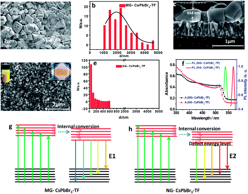 |
| | Fig. 3 (a) SEM images of MG-CsPbBr3-TF. (b) The statistical distribution of grain size in MG-CsPbBr3-TF. (c) Cross-sectional SEM images of MG-CsPbBr3-TF. (d) SEM images of NG-CsPbBr3-TF. (e) The statistical distribution of grain size in NG-CsPbBr3-TF. (f) The photoluminescence (PL) spectra of MG-CsPbBr3-TF and NG-CsPbBr3-TF thin films. Schematic energy level diagrams of (g) MG-CsPbBr3-TF and (h) NG-CsPbBr3-TF. | |
To investigate the photoelectric properties of the MG-CsPbBr3-TF thin film, photodetectors based on MG-CsPbBr3-TF were prepared. The preparation procedure of such devices is shown in Fig. 4. The device structure is FTO/TiO2/CsPbBr3/carbon electrode. External quantum efficiencies (EQE) were measured, as shown in Fig. 4a. The MG-CsPbBr3-TF film exhibited EQE from 330 nm to 510 nm, which corresponded to the absorption range of the UV absorption spectrum (Fig. 2b). The device based on the thin film prepared at 300 °C on TiO2-ECL only exhibited EQE from 300 nm to 400 nm. The device based on the thin film prepared at 100 °C on TiO2-ECL exhibited zero EQE from 300 to 800 nm. The on–off performance of the devices based on MG-CsPbBr3-TF under different wavelengths of the monochromatic light was investigated. The device exhibited significant on–off photocurrent responses with on–off operation at 330, 360, 390, 410, 420, 450, 480, 510, 540, 570 and 600 nm, as shown in Fig. 4b, c and S1.† As is well-known, the poor stability of organic–inorganic perovskites seriously restricts their commercialization. Meanwhile, all-inorganic perovskites are expected to have improved stability. The stability of MG-CsPbBr3-TF stored in the air (T = 298 K, 40% humidity) was tested by obtaining its UV absorption spectrum. No clear change in the absorption intensity was observed after nearly 2000 h of storage. The device stability data are shown in Fig. S2.† The device placed in the air for 7 months still exhibited clear photoresponse under AM1.5, 100 mW cm−2 simulated illumination. These results confirmed that MG-CsPbBr3-TF possessed good stability. In addition, CsPbBr3 single crystals were prepared from CsPbBr3/HBr supernatant, as shown in Fig. S3.† The thermal stability of CsPbBr3 single crystals was assessed by thermogravimetric analysis (Fig. S4†). The results indicated that CsPbBr3 single crystal materials begin to decompose at 500 °C. Compared with organic–inorganic hybrid CH3NH3PbI3 materials, inorganic CsPbBr3 perovskites indeed exhibited good thermal stability.
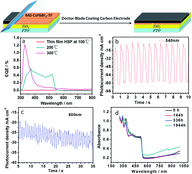 |
| | Fig. 4 (a) External quantum efficiency (EQE) of FTO/TiO2/CsPbBr3/carbon electrode device prepared on TiO2-ECL at different temperatures. (b) Photocurrent density–time characteristics of the FTO/TiO2/CsPbBr3/carbon electrode device under 540 nm wavelength. (c) Photocurrent density–time characteristics of the FTO/TiO2/CsPbBr3/carbon electrode device under 600 nm wavelength. (d) UV-Vis absorption spectra of MG-CsPbBr3-TF stored in the air (T = 298 K, 40% humidity). | |
Conflicts of interest
There are no conflicts to declare.
Acknowledgements
This work was financially supported by Shandong Province Natural Science Foundation (Grant No. ZR2016BQ20; BS2015NJ013; ZR2014BQ010; ZR2016BQ21), Colleges and Universities in Shandong Province Science and Technology projects (Grant No. J16LC05; J17KA097), Science and Technology Innovation Foundation for the University or College students (Grant No. 26312160502), National Science and Technology Innovation Foundation for the University or College Students (Grant No. 201510447021), Research Fund for the Doctoral Program of Liaocheng University (Grant No. 31805), National Natural Science Foundation of China (Grant No. 21503104; 21601078, 21401095), National Basic Research Program of China (Grant No. 2011CBA00701).
References
- V. D'Innocenzo, G. Grancini, M. J. P. Alcocer, A. R. S. Kandada, S. D. Stranks, M. M. Lee, G. Lanzani, H. J. Snaith and A. Petrozza, Excitons versus free charges in organo-lead tri-halide perovskites, Nat. Commun., 2014, 5, 3586 CrossRef PubMed.
- A. Kojima, K. Teshima, Y. Shirai and T. Miyasaka, Organometal Halide Perovskites as Visible-Light Sensitizers for Photovoltaic Cells, J. Am. Chem. Soc., 2009, 131(17), 6050–6051 CrossRef PubMed.
- S. D. Stranks, G. E. Eperon, G. Grancini, C. Menelaou, M. J. P. Alcocer, T. Leijtens, L. M. Herz, A. Petrozza and H. J. Snaith, Electron-Hole Diffusion Lengths Exceeding 1 Micrometer in an Organometal Trihalide Perovskite Absorber, Science, 2013, 342(6156), 341–344 CrossRef PubMed.
- G. Xing, N. Mathews, S. Sun, S. S. Lim, Y. M. Lam, M. Graetzel, S. Mhaisalkar and T. C. Sum, Long-Range Balanced Electron- and Hole-Transport Lengths in Organic-Inorganic CH3NH3PbI3, Science, 2013, 342(6156), 344–347 CrossRef PubMed.
- W. S. Yang, B. W. Park, E. H. Jung, N. J. Jeon, Y. C. Kim, D. U. Lee, S. S. Shin, J. Seo, E. K. Kim, J. H. Noh and S. I. Seok, Iodide management in formamidinium-lead-halide-based perovskite layers for efficient solar cells, Science, 2017, 356(6345), 1376–1379 CrossRef PubMed.
- M. Kulbak, D. Cahen and G. Hodes, How Important Is the Organic Part of Lead Halide Perovskite Photovoltaic Cells? Efficient CsPbBr3 Cells, J. Phys. Chem. Lett., 2015, 6(13), 2452–2456 CrossRef PubMed.
- C. C. Stoumpos, C. D. Malliakas, J. A. Peters, Z. Liu, M. Sebastian, J. Im, T. C. Chasapis, A. C. Wibowo, D. Y. Chung, A. J. Freeman, B. W. Wessels and M. G. Kanatzidis, Crystal Growth of the Perovskite Semiconductor CsPbBr3: A New Material for High-Energy Radiation Detection, Cryst. Growth Des., 2013, 13(7), 2722–2727 CrossRef.
- X. L. Zhang, B. Xu, J. B. Zhang, Y. Gao, Y. J. Zheng, K. Wang and X. W. Sun, All-Inorganic Perovskite Nanocrystals for High-Efficiency Light Emitting Diodes: Dual-Phase CsPbBr3-CsPb2Br5 Composites, Adv. Funct. Mater., 2016, 26(25), 4595–4600 CrossRef.
- Y. F. Xu, M. Z. Yang, B. X. Chen, X. D. Wang, H. Y. Chen, D. B. Kuang and C. Y. Su, A CsPbBr3 Perovskite Quantum Dot/Graphene Oxide Composite for Photocatalytic CO2 Reduction, J. Am. Chem. Soc., 2017, 139(16), 5660–5663 CrossRef PubMed.
- J. Z. Song, J. H. Li, X. M. Li, L. M. Xu, Y. H. Dong and H. B. Zeng, Quantum Dot Light-Emitting Diodes Based on Inorganic Perovskite Cesium Lead Halides (CsPbX3), Adv. Mater., 2015, 27(44), 7162–7167 CrossRef PubMed.
- G. Nedelcu, L. Protesescu, S. Yakunin, M. I. Bodnarchuk, M. J. Grotevent and M. V. Kovalenko, Fast Anion-Exchange in Highly Luminescent Nanocrystals of Cesium Lead Halide Perovskites (CsPbX3, X = Cl, Br, I), Nano Lett., 2015, 15(8), 5635–5640 CrossRef PubMed.
- L. Protesescu, S. Yakunin, M. I. Bodnarchuk, F. Krieg, R. Caputo, C. H. Hendon, R. X. Yang, A. Walsh and M. V. Kovalenko, Nanocrystals of Cesium Lead Halide Perovskites (CsPbX3, X = Cl, Br, and I): Novel Optoelectronic Materials Showing Bright Emission with Wide Color Gamut, Nano Lett., 2015, 15(6), 3692–3696 CrossRef PubMed.
- J. H. Li, L. M. Xu, T. Wang, J. Z. Song, J. W. Chen, J. Xue, Y. H. Dong, B. Cai, Q. S. Shan, B. N. Han and H. B. Zeng, 50-Fold EQE Improvement up to 6.27% of Solution-Processed All-Inorganic Perovskite CsPbBr3 QLEDs via Surface Ligand Density Control, Adv. Mater., 2017, 29(5), 1603885 CrossRef PubMed.
- A. Swarnkar, R. Chulliyil, V. K. Ravi, M. Irfanullah, A. Chowdhury and A. Nag, Colloidal CsPbBr3 Perovskite Nanocrystals: Luminescence beyond Traditional Quantum Dots, Angew. Chem., Int. Ed., 2015, 54(51), 15424–15428 CrossRef PubMed.
- K. F. Wu, G. J. Liang, Q. Y. Shane, Y. P. Ren, D. G. Kong and T. Q. Lian, Ultrafast Interfacial Electron and Hole Transfer from CsPbBr3 Perovskite Quantum Dots, J. Am. Chem. Soc., 2015, 137(40), 12792–12795 CrossRef PubMed.
- H. Zhou, Z. Nie, J. Yin, Y. Sun, H. Zhuo, D. Wang, D. Li, J. Dou, X. Zhang and T. Ma, Antisolvent diffusion-induced growth, equilibrium behaviours in aqueous solution and optical properties of CH3NH3PbI3 single crystals for photovoltaic applications, RSC Adv., 2015, 5(104), 85344–85349 RSC.
- D. J. Liu, Z. P. Hu, W. Hu, P. H. Wangyang, K. Yu, M. Q. Wen, Z. Q. Zu, J. Liu, M. Wang, W. W. Chen, M. Zhou, X. S. Tang and Z. G. Zang, Two-step method for preparing all-inorganic CsPbBr3 perovskite film and its photoelectric detection application, Mater. Lett., 2017, 186, 243–246 CrossRef.
- D. N. Dirin, I. Cherniukh, S. Yakunin, Y. Shynkarenko and M. V. Kovalenko, Solution-Grown CsPbBr3 Perovskite Single Crystals for Photon Detection, Chem. Mater., 2016, 28(23), 8470–8474 CrossRef PubMed.
- J. X. Ding, S. J. Du, Z. Y. Zuo, Y. Zhao, H. Z. Cui and X. Y. Zhan, High Detectivity and Rapid Response in Perovskite CsPbBr3 Single-Crystal Photodetector, J. Phys. Chem. C, 2017, 121(9), 4917–4923 CrossRef.
- M. I. Saidaminov, M. A. Haque, J. Almutlaq, S. Sarmah, X. H. Miao, R. Begum, A. A. Zhumekenov, I. Dursun, N. Cho, B. Murali, O. F. Mohammed, T. Wu and O. M. Bakr, Inorganic Lead Halide Perovskite Single Crystals: Phase-Selective Low-Temperature Growth, Carrier Transport Properties, and Self-Powered Photodetection, Adv. Opt. Mater., 2017, 5(2), 1600704 CrossRef.
- Z. H. Nie, J. Yin, H. W. Zhou, N. Chai, B. L. Chen, Y. T. Zhang, K. G. Qu, G. D. Shen, H. Y. Ma, Y. C. Li, J. S. Zhao and X. X. Zhang, Layered and Pb-Free Organic-Inorganic Perovskite Materials for Ultraviolet Photoresponse: (010)-Oriented (CH3NH3)(2)MnCl4 Thin Film, ACS Appl. Mater. Interfaces, 2016, 8(41), 28187–28193 CrossRef PubMed.
Footnote |
| † Electronic supplementary information (ESI) available. See DOI: 10.1039/c8ra04558e |
|
| This journal is © The Royal Society of Chemistry 2018 |
Click here to see how this site uses Cookies. View our privacy policy here. 
 Open Access Article
 This Open Access Article is licensed under a Creative Commons Attribution-Non Commercial 3.0 Unported Licence
 *a,
Lin Fana,
Guohang Hea,
Cang Yuana,
Yunying Wanga,
Shaozhen Shia,
Ning Suib,
Baoli Chen
*a,
Lin Fana,
Guohang Hea,
Cang Yuana,
Yunying Wanga,
Shaozhen Shia,
Ning Suib,
Baoli Chen


