DOI:
10.1039/C8RA04355H
(Paper)
RSC Adv., 2018,
8, 30310-30319
A solution-processed tin dioxide film applicable as a transparent and flexible humidity sensor
Received
22nd May 2018
, Accepted 18th August 2018
First published on 28th August 2018
Abstract
An all-solution-processed transparent tin oxide (SnO2)-based humidity sensor was directly prepared on borosilicate glass (SnO2–G) and a flexible polyethylene terephthalate (SnO2–PET) substrate without using a template. The entire process included film deposition by a spin-spray process at 90 °C and subsequent hot water treatment (HWT) at 100 °C. The resistivity of the films dramatically decreased and had semiconductor characteristics after the HWT, even though the as-prepared SnO2–G and SnO2–PET samples were insulators. Based on the results, the variation of the resistivity could be attributed to the formation of a hydroxyl layer on the crystallized SnO2 surface. With the help of the HWT on the SnO2 films, the formation of tin hydroxyl derivatives provided mobile protons, which led to the variation of the electrical properties of SnO2 at ambient conditions with different humidities. The sensitivity of the SnO2–G-HWT and SnO2–PET-HWT at 95% relative humidity (RH) was 35.2 and 3.5 times higher, respectively, than that at 5% RH. Both the sensitivity of the SnO2–G-HWT and SnO2–PET-HWT samples showed a good uptrend corresponding to the increase of RH at 20 ± 1 °C, and the response/recovery time of SnO2–G-HWT and SnO2–PET-HWT was 51/38 s and 69/47 s in the % RH range of 30–70% at 20 ± 1 °C, respectively.
1. Introduction
Metal-oxide-semiconductor-based sensors have received much attention during the past decade owing to their sensitivity and the easy modification of their properties by varying the external conditions including chemical, physical or biological effects. In recent years, electronic devices that possess both transparency and flexibility have received even more interest owing to the wider applicability in different shapes. As one of the prospective materials for use in sensors, SnO2 has been the subject of extensive research and development because of its outstanding properties such as good electrical and optical properties, high sensitivity, fast response, and low cost.1,2 Several studies dedicated to improving the efficacy of SnO2-based sensors by the addition of a dopant or control of the surface morphology have been reported and have proved that SnO2-based materials could be employed in a wide range of applications including gas, humidity, or biomedical sensors with high performance.3–8 However, owing to the unavoidable requirement of relatively high process temperature for the fabrication of SnO2 films and the low heat-resistant temperature of the general polymer substrate (e.g., polyethylene terephthalate, polyethylene naphthalate, polyethersulfone), it is still an insurmountable obstacle to directly prepare a SnO2 film on a flexible substrate.9 A simple method for synthesizing SnO2 films was provided by Vayssieres and Graetzel in 2004. A film consisting of a homogeneous dispersion of crystalline SnO2 nanorods was successfully fabricated at 95 °C by conducting a low temperature hydrothermal process for 2 days.10 Thereafter, Her et al. investigated the material properties and luminescence phenomenon of SnO2 films with respect to the process conditions.11 However, the process still took one day for the deposition of the film only 100 nm in thickness. To the best of our knowledge, these are the only two examples of the successful fabrication of SnO2 film on non-seeded substrates below 100 °C without post heat treatment (>100 °C). Therefore, further research is required for the development of a low-temperature process for the fabrication of SnO2 films, and it is also strongly required to understand the relationship between the process conditions and the film properties.
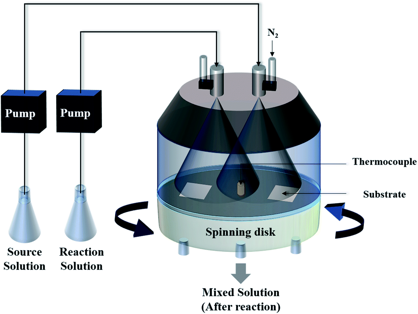
Herein, we present a two-step but more efficient method for the synthesis of a SnO2 film on a non-seeded substrate at a temperature below 100 °C. First, the SnO2 films were deposited by a spin-spray process, as shown in Fig. 1. The spin-spray technique has been applied for the preparation of ferrite films for noise suppressors.12 The spin-spray process could supply a continuous fresh solution to avoid the inconstant concentration of the precursor solution. In addition, because the formation of free nuclei would be removed from the spinning disk, the nuclei could selectively grow on the substrate. These effects of the spin-spray technique led to a relatively higher deposition rate and crystal quality of the deposited films. Similarly, a high-speed fabrication of crystallized ZnO film was successfully accomplished by a spin-spray method in 2010.13 It should be noted that the spin-spray process possesses relatively approachable process conditions including low operating temperature (≤100 °C) and the ability of working at atmospheric pressure. The vacuum systems and the relatively high-power supply machines are not required in spin-spray process. Compared with the sputtering, thermal evaporation and chemical vapor deposition process which are often used to prepare the SnO2 films, the spin-spray process could be regarded as a relative low-cost synthesis method. Therefore, the spin-spray process has a great potential for application to other kinds of material. After the preparation of the SnO2 films, the samples were placed in an oven for hot water treatment (HWT) at 100 °C. HWT is a simple low temperature (≤100 °C) solution process that can be used to rapidly fabricate a crystallized oxide layer on a metal surface in pure boiling water. Lamberti et al. first demonstrated that crystallized TiO2 nanotubes could be prepared on a titanium surface by a HWT process.14 Afterward, a systematic investigation of HWT of several kinds of metal was performed by Saadi et al., which showed that HWT could effectively trigger the oxidation reaction, crystallization, and morphological architecture of numerous elements.15 Because most of the research has focused on the effect of HWT for the formation of crystallized oxides on a metal surface, there has been limited investigations of the effect of HWT on metal oxides. Nose et al. demonstrated the reaction of the oxidation state transformation from crystallized SnO to amorphous SnO2 by using HWT.16 However, the crystallization and phase transformation reaction of SnO2 were strongly influenced by the process conditions; therefore, the reported methods might not always be suitable for films prepared by different processes. Therefore, it is worth performing further research to classify the reaction mechanism of solution-processed SnO2 films at a relatively low temperature. Inspired by the reasons mentioned above, we first demonstrated a novel two-step method including film deposition at 90 °C and a post HWT process at 100 °C for the fabrication of a transparent SnO2 film on both glass and flexible PET substrates. The material properties and the humidity sensing properties of SnO2 films were investigated, and the effect of the HWT process on the SnO2-based humidity sensor are discussed in this study.
 |
| | Fig. 1 A schematic diagram of the spin-spray apparatus. | |
2. Materials and methods
2.1 SnO2 film fabrication and HWT process
SnO2 films were deposited on borosilicate glass and flexible PET substrates. Before deposition, the substrates were sonicated in deionized water, ethanol, acetone, and deionized water for 5 min to remove impurities on the substrate surface. Afterward, the substrates were placed into a UV-Ozone cleaner (BIOFORCE nanosciences, UV Ozone Cleaner ProCleaner™ Plus) for further 30 min. The SnO2 films were deposited by a spin-spray process using stannous fluoride (SnF2, 97%, Morita Chemical Industries co., Ltd.) and sodium nitrate (NaNO3, 99.0%, Wako Pure Chemical Industries, Ltd.). These precursor materials were dissolved in 1.0 L deionized water. They were used as a Sn ion source solution and reaction solution, respectively. The chemical reactions between the source solution and the reaction solution are showing below.| | |
3Sn(OH)2 + 2NaNO3 + 2H+ → 3SnO2 + 2NO + 2Na+ + 4H2O
| (1) |
| | |
Sn(OH)2 + 2NaNO3 + 2H+ → SnO2 + 2NO2 + 2Na+ + 2H2O
| (2) |
During spin-spray, the sample stage was heated to 90 °C and kept rotating at 120 rpm. The spray solution (SnF2 and NaNO3 solution) was mixed together at a molar ratio of 1![[thin space (1/6-em)]](https://www.rsc.org/images/entities/char_2009.gif) :1. All the chemical compounds were employed in the deposition without further refinement. After the deposition, the SnO2 film samples were thoroughly washed by deionized water to remove any contaminants on the sample surface.
:1. All the chemical compounds were employed in the deposition without further refinement. After the deposition, the SnO2 film samples were thoroughly washed by deionized water to remove any contaminants on the sample surface.
Samples with and without the post HWT process were prepared for comparison. The HWT method was carried out by placing the SnO2–G and SnO2–PET samples into a glass beaker containing 100 mL deionized water and sealed with a plastic wrap. The SnO2 samples were heated in deionized water by a regular laboratory oven at 100 °C for 12 h and cooled down to room temperature (20 °C) naturally. Afterward, all the samples were dried in an oven at 60 °C for 1 h. As a control group, the samples that did not undergo the post HWT process were directly placed in the oven and dried at 60 °C for 1 h. The reason why the drying process was applied is to remove the remained water molecular on SnO2 sample surface which formed during HWT process. The research results have revealed that the drying process at 60 °C for 1 h would not damage the Sn–OH derivatives formed on SnO2 surface, and the SnO2 layer humidity sensor could still work effectively after conducting this approach. Besides, to rule out the possibility that the substrate might reveal the humidity sensing behaviour. The HWT process was also applied on untreated borosilicate glass and PET substrate. The results revealed that both the borosilicate glass and PET substrate did not show any conductive or semiconductor conductive characteristics while examining by LCR meter at 20 ± 1 °C before or after HWT. Therefore, we believed that the influence of both borosilicate glass and PET substrate during sensitivity measurement could be neglected.
2.2 Characterization
The surface morphology and cross-section of SnO2 were observed by field emission scanning electron microscopy (FE-SEM, HITACHI, S-4700) in secondary electron mode with a working voltage 8 kV. The crystallinity and microstructure were analyzed by an X-ray diffractometer (XRD, BRUKER co., D8 FOCUS/TXS) at a scan angle (2θ) range of 20 to 80°. The X-ray was generated by a Cu-Kα target operated at 35 kV and 300 mA with a wavelength of 0.15418 nm. The chemical state of the SnO2 films was examined by X-ray photoelectron spectroscopy (XPS, Physical Electronics, Inc., PHI 5000). Fourier-transfer infrared spectroscopy (FTIR, SHIMADZU co., IRPrestige-21) was carried out by mixing the peeled SnO2 powder (1 mg) with potassium bromide (KBr, 300 mg) to evaluate the variation in the chemical composition of the SnO2 film before and after HWT for comparison. In addition, the transparency and absorbance of SnO2 in the ultraviolet-visible (UV-vis) region were evaluated by a V-570 spectrophotometer (JASCO).
2.3 Measurement of the humidity sensing
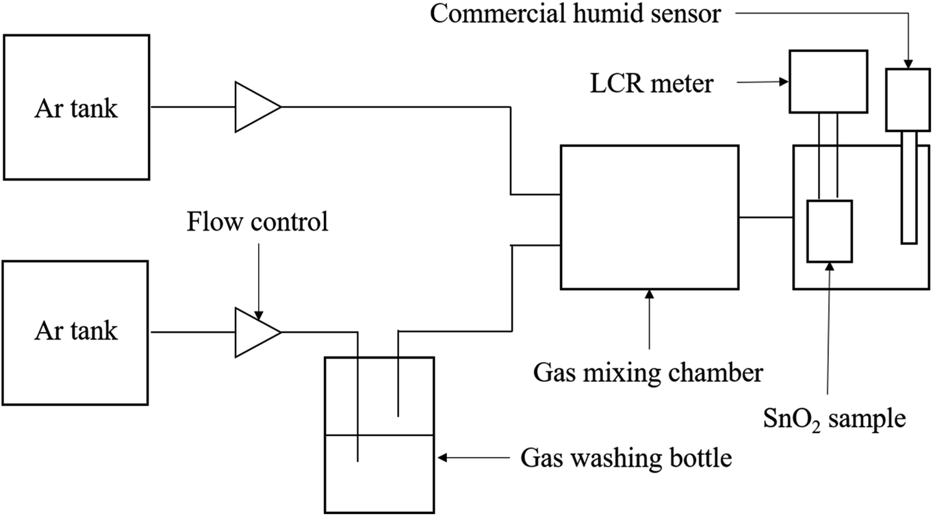
The resistivity measurements of SnO2-based sensor corresponding to different RH were carried out at 20 ± 1 °C in a sealed three-neck flask. The RH values were controlled by using saturated salt solutions of CH3COOK, K2CO3, NaBr, NaCl, and K2NO3, which yielded humidity levels of 23%, 43%, 59%, 75%, and 95%, respectively.17,18 All the saturated solutions were kept overnight in the flask to ensure the humidity environment reached an equilibrium before measurement. A dried atmosphere was obtained by placing solid NaOH (5% RH) in a closed flask.19,20 A standard hydrometer was employed for confirming the precision of the relative humidity. The electrical resistance of the sensing material was measured by a basic 2 probe LCR meter (inductance (L), capacitance (C), and resistance (R)) in DC resistance mode under different humidity conditions, and the distance between the two measurement points was maintained at 10 mm. The sensitivity of the SnO2–G and SnO2–PET were defined as S = (R0 − R)/R0, in which R0 is the resistance of SnO2 at 5% RH. In addition, the examination of humidity response and recovery time were carried out by using the 2 probe LCR meter to measure the resistance change of both the SnO2–G and SnO2–PET samples during the humidification from 30 to 70% RH as well as the desiccation from 70 to 30% RH at 20 ± 1 °C. The scheme of sensing property measurement system was illustrated in Fig. 2. The RH% value was controlled by mixing the dry and humidified argon gas flow, and the flow rate was kept at 100 sccm.
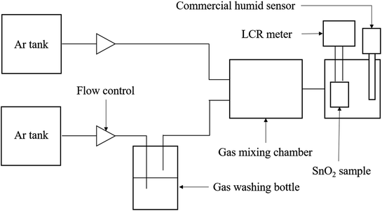 |
| | Fig. 2 The scheme of the sensing property measurement system. | |
3. Results and discussions
3.1 The optical properties of SnO2–G and SnO2–PET
The transmittance and absorbance spectrum of SnO2 before and after HWT were examined by a UV-vis spectrometer and shown in Fig. 3. According to Fig. 3(A), the SnO2–G film had a higher transmittance than SnO2–PET owing to the difference in the pristine transparency of the glass and PET substrates. The pristine transparency of borosilicate glass and the PET substrate were 90% and 70%, respectively, within the visible light wavelength range. Both SnO2–G and SnO2–PET showed a slight decrease in transparency after undergoing the HWT process. The reasonable explanations for this phenomenon were the formation of defects inside the SnO2 layer on the surface layer during the HWT process. The formation of these defects would cause the scattering of light and lead to a decrease in transparency. The insets (a) and (b) in Fig. 3(A) are photos of SnO2–G and SnO2–PET samples that underwent HWT for 12 h, which show the semitransparent characteristics. As shown in Fig. 3(B), the energy band gap of SnO2–G and SnO2–PET were 3.40 and 3.35 eV, respectively, which were slightly lower than the typical band gap of SnO2 at 3.50 eV. In addition, there was no obvious change of energy band gap of the samples before and after the HWT process.
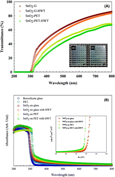 |
| | Fig. 3 The optical properties of the SnO2 samples. (A) The transmittance results for SnO2. The inset photographs show (a) SnO2–G and (b) SnO2–PET samples after the HWT process. (B) The absorbance and band-gap spectra. | |
3.2 Elemental analysis of SnO2–G and SnO2–PET
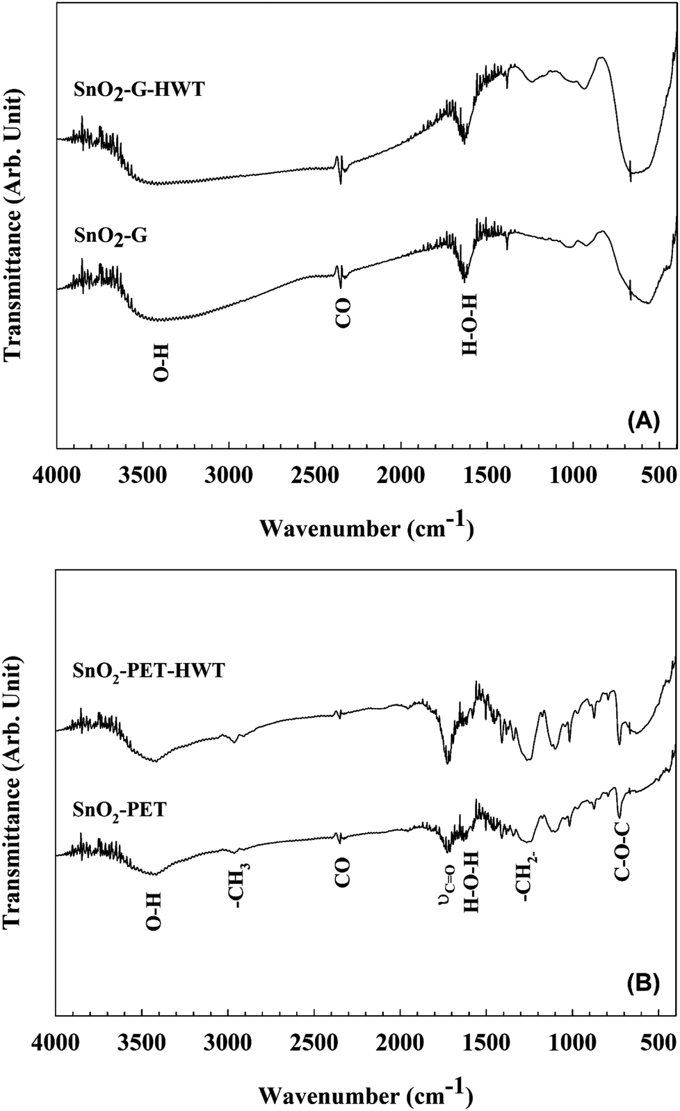
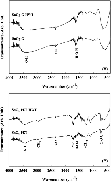
To clarify the effects of the HWT process on the SnO2 film, FTIR studies were carried out to compare the variation of the chemical composition before and after HWT. As shown in Fig. 4(A), both the SnO2–G and SnO2–G-HWT samples revealed a peak located at 1638 cm−1 and a broad band at approximately 2500–3600 cm−1, which corresponded to the bending mode of the H–O–H bond groups of the adsorbed water molecules and the stretching vibrations of the hydroxyl groups (Sn–OH, bridged bonding), respectively.21,22 It was found there was no significant change of these two bands corresponding to water content before and after HWT. This might result from the usage of KBr in the FTIR measurement since the adsorption behaviour of the water molecular on KBr would lead to the interference of IR transmittance measurement.23 Further examinations for defining the water content on the SnO2 surface were carried out and would be discussed in the next section. The broad band located between 500 and 800 cm−1 was attributed to the overlapping of the Sn–O–Sn, O–Sn–O, Sn–OH bands or the symmetric and asymmetric stretching vibration bands of SnO2.22,24–26 The increase of the band intensity was attributed to the transformation reaction from tin hydroxide to tin oxide and the bonding of the newly formed hydroxyl species with the crystallized SnO2 phase during HWT.27
 |
| | Fig. 4 The FT-IR spectra of SnO2. (A) SnO2–G before and after the HWT process, (B) SnO2–PET before and after the HWT process. | |
The FTIR spectra of SnO2–PET before and after the HWT process are shown in Fig. 4(B). Similar to the SnO2–G samples, the peak at 1640 cm−1 and broad band in the range of 3100–3600 cm−1 indicated the presence of adsorbed water and the adsorbed hydroxide, and the further confirmations for the formation of the adsorbed hydroxide were carried out and would be discussed in the next section. The results of SnO2–PET and SnO2–PET-HWT revealed several peaks corresponding to PET, including the ethers (C–O–C) at 716 cm−1, methanediyl (–CH2–) at 1250 cm−1, the stretching vibration band of the C![[double bond, length as m-dash]](https://www.rsc.org/images/entities/char_e001.gif) O group at 1730 cm−1, and the methyl (–CH3) at 2970 cm−1.28,29 The broad band located within 400–700 cm−1 became stronger for the SnO2–PET samples underwent the HWT process. Similarly, this broad band was attributed to overlapping of the tin hydroxide species, Sn–O–Sn, and O–Sn–O peaks or the symmetric and asymmetric stretching vibration bands of SnO2. The increase of the band intensity might be induced by the formation of tin hydroxyl groups and SnO2 during the HWT process.
O group at 1730 cm−1, and the methyl (–CH3) at 2970 cm−1.28,29 The broad band located within 400–700 cm−1 became stronger for the SnO2–PET samples underwent the HWT process. Similarly, this broad band was attributed to overlapping of the tin hydroxide species, Sn–O–Sn, and O–Sn–O peaks or the symmetric and asymmetric stretching vibration bands of SnO2. The increase of the band intensity might be induced by the formation of tin hydroxyl groups and SnO2 during the HWT process.
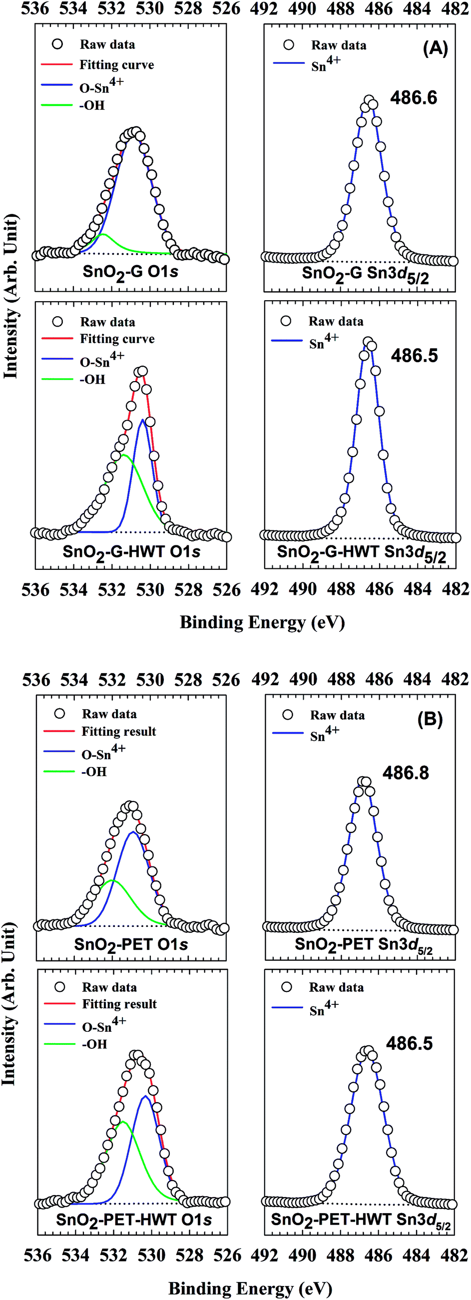
3.3 The chemical state of SnO2–G and SnO2–PET
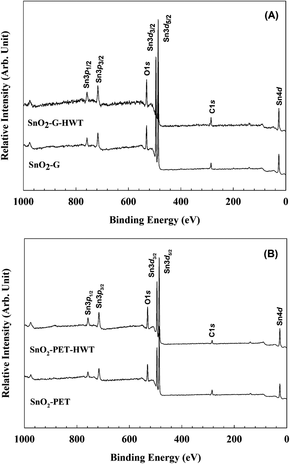
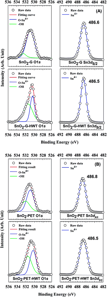
The chemical state of SnO2–G and SnO2–PET samples with and without undergoing the HWT process were examined and evaluated by XPS, and the spectra are presented in Fig. 4. All the XPS data were calibrated to the C1s peak at 284.6 eV arising from the residual carbon on the sample surface. Besides, all the assigned peak positions for curve fitting were based on the Handbook of X-ray photoelectron spectroscopy.30 According to Fig. 5(A) and (B), the peaks corresponding to Sn4d, C1s, Sn3d, O1s, and Sn3p were observed in the SnO2–G and SnO2–PET samples; in addition, impurities such as F, Na, and Si were not observed by the XPS survey spectrum. Fig. 6(A) and (B) demonstrate that the oxidation state of the SnO2–G and SnO2–PET samples were mainly Sn4+ with a binding energy of approximately 486.6 eV. The O1s peak was composed of O–Sn4+ and –OH bonding, corresponding to 530.9 and 532.0 eV, respectively. Both the SnO2–G and SnO2–PET samples were in the O–Sn4+ state with tin hydroxide. Interestingly, the percentage of hydroxide concentration for both SnO2–G and SnO2–PET samples increased after the HWT process. We attributed this to the reaction of the surface of the SnO2 layer with dissociated water and the formation of a thin layer of hydroxyl derivatives (Sn(OH)x) during the HWT process. Therefore, a considerable increase in the tin hydroxide signal was observed after HWT.
 |
| | Fig. 5 The XPS survey spectrum of (A) SnO2–G and (B) SnO2–PET. | |
 |
| | Fig. 6 The XPS spectrum of SnO2 samples at binding energies of O1s and Sn3d5/2 for SnO2–G and SnO2–PET samples before and after the HWT process. | |
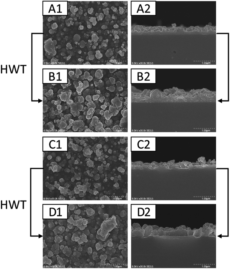
3.4 Effects of the HWT process on SnO2
Fig. 7 shows the surface morphology and cross-section characteristics of SnO2–G and SnO2–PET prepared under the different process conditions (with or without the HWT process) under 30k× magnification. The results revealed that both SnO2–G or SnO2–PET without HWT formed spherical nanoparticles. The particle size ranged from approximately 100 to 500 nm. After the HWT process, both the morphology of SnO2–G and SnO2–PET revealed the same particle-like morphology. However, the surface after the HWT process was less uniform. The coalescence phenomenon between the SnO2 particles was found after HWT process. It could be attributed to the Ostwald ripening effect which led to the attachment of the crystallographically oriented tiny SnO2 particles and formed a larger one. According to Fig. 7(A2) and (B2), the SnO2–G-HWT exhibited a rough surface compared with that of the SnO2–G sample, and the average thickness was approximately 400 nm, which was thicker than the average 250 nm of the SnO2–G sample. The average thickness of the SnO2–PET-HWT was nearly the same as that of the SnO2–G-HWT sample, and thicker than the 200 nm thickness of the as-prepared SnO2–PET film. The variation of the thickness and surface morphology were presumed to be induced by the transformation reaction from tin hydroxide to tin oxide, the new formation of tin hydroxide on the surface layer and the Ostwald ripening effect.
 |
| | Fig. 7 The surface morphology and cross-section characteristics of SnO2–G and SnO2–PET samples. (A1), (B1), (C1), and (D1) show the surface morphology of SnO2–G, SnO2–G-HWT, SnO2–PET, and SnO2–PET-HWT, respectively. (A2) and (C2) are the cross-section images of SnO2–G and SnO2–PET before HWT, respectively. (B2) and (D2) show the cross-section of SnO2–G and SnO2–PET after HWT, respectively. | |
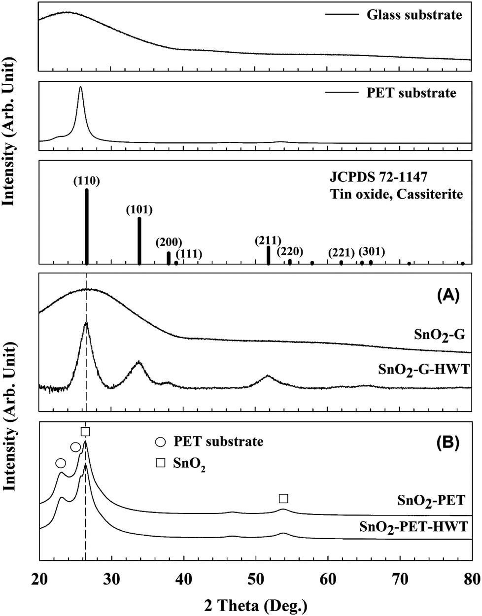
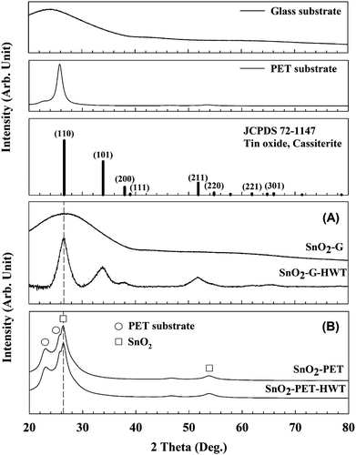
To realize the crystallinity and microstructure of SnO2, XRD measurements were performed and the results are shown in Fig. 8. The SnO2–G samples were amorphous before the HWT process, which coincided with the research reported by Uchiyama et al.31 According to the literature, amorphous tin oxide or hydroxide powders can be prepared at intermediate pH ranging from 4 to 7 using an SnF2 precursor solution. The SnO2 samples became crystallized cassiterite tin dioxide (JCPD # 72-1147) after conducting the HWT process for 12 h. The XRD pattern of SnO2–G comprised peaks at 26.5°, 33.8°, 38.9°, and 51.7° associated with the (hkl) planes (110), (101), (200), and (211), respectively. Similar XRD results were reported by Mikhaylov et al.32 In contrast, there was no clear difference in the XRD pattern of SnO2–PET before and after the HWT process. In other words, both the as-prepared SnO2–PET and SnO2–PET-HWT samples were crystalline. The broad band within 20–30° was the overlapping peaks for PET and SnO2. The main peak at 26.5° indicated the (110) orientation of SnO2, and the shoulder peaks located at 23.1° and 25.7° were attributed to the PET substrate.33 In contrast to SnO2–G, there were only two growth orientations, (110) and (220), for the SnO2–PET sample, which were located at 26.5° and 54.7°, respectively.
 |
| | Fig. 8 The XRD patterns of SnO2 (JCPD 72-1147), the glass and PET substrate. (A) XRD patterns of the glass substrate and SnO2–G before and after the HWT process, (B) XRD patterns of the SnO2–PET before and after the HWT process. | |
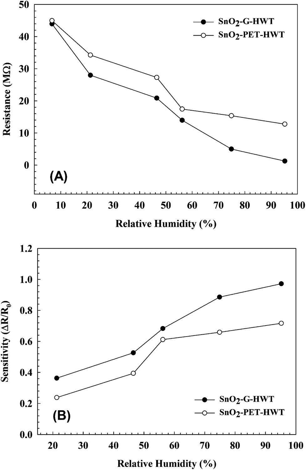
3.5 Sensing properties of SnO2–G and SnO2–PET
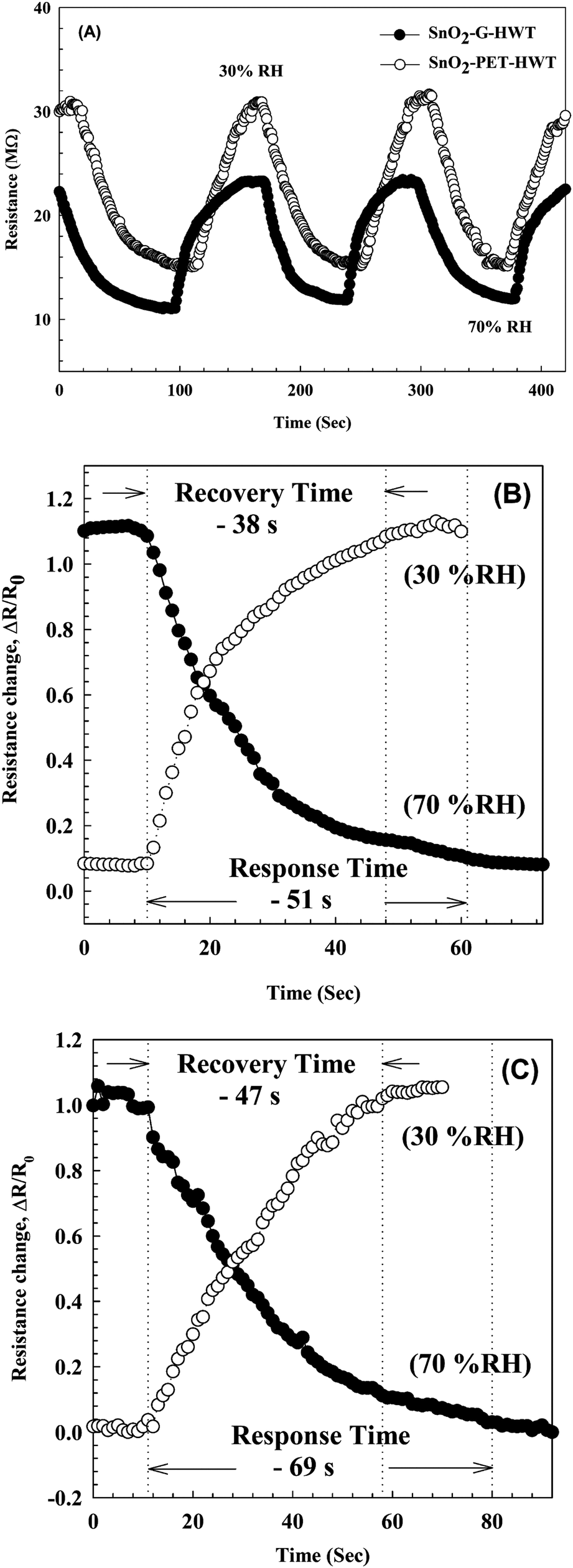
The sensing properties of the SnO2–G-HWT and SnO2–PET-HWT are shown in Fig. 9. According to Fig. 9(A), the variation of the DC resistance of SnO2–G-HWT and SnO2–PET-HWT exhibited a downward trend with respect to the increase of % RH (5–95%). There was no significant difference in the resistance of SnO2–G-HWT and SnO2–PET-HWT at low RH%; however, the discrepancy became larger at higher RH%. The resistance of SnO2–G-HWT and SnO2–PET-HWT was 1.25 and 12.74 MΩ at 95% RH, which was 35.2 and 3.5 times lower compared to the resistance of SnO2–G-HWT and SnO2–PET-HWT at 5% RH, respectively. This considerable variation of resistance indicated that the water on the surface strongly influenced the condition of the film and led to a higher conductivity of SnO2. Compared with the SnO2–G-HWT sample, the SnO2–PET-HWT sample exhibited the smaller change amount of resistance corresponding to the variation of RH%, which might be caused by the cracks inside the SnO2 layer owing to the unavoidable bending stress during the experiment, which would lead to the higher resistance and the worse electron transportation. Fig. 9(B) illustrates the sensitivity results of the SnO2–G-HWT and SnO2–PET-HWT samples with respect to different % RH at room temperature. As expected, both the sensitivity of SnO2–G-HWT and SnO2–PET-HWT revealed a linear upward tendency corresponding to the increase of % RH. It is known H2O could absorb on the SnO2 surface in molecular or dissociative forms,34 and the water adsorption mechanism on ceramic oxide surfaces could be generalized by the formation of chemisorbed hydroxide layers followed by the physisorbed layers.35 According to the XPS results shown in Fig. 6, SnO2 and Sn–OH groups with a chemical state of Sn4+ existed, and the signal intensity of Sn–OH became stronger after samples underwent the HWT process. Herein, the HWT process performed in deionized water could be regarded as a 100% RH environment at 100 °C (self-ionization constant of water at 100 °C, Kw = 55.0 × 10⁻¹⁴). During the process, the as-prepared SnO2–G layer would first crystallize, and the water molecular would chemisorb at the neck side of both the SnO2–G and SnO2–PET crystalline grains. Afterward, the lattice oxygen on the SnO2 surface was replaced and formed a Sn–OH group layer, which is the dissociative water that would be physisorbed on the SnO2 film surface. The significant formation of tin hydroxyl groups possessing a high charge carrier density and strong electrostatic fields could provide mobile protons, singly bond with water molecules, and lead to the variation of the resistance. Because the HWT process was operated in water at 100 °C, the formation of a physisorbed hydroxyl layer would still exist after the HWT process. Consequently, we believed that the movable H proton in hydrogenated SnO2 particle could act as the donor on the SnO2 layer surface and influence the surface chemical/electrical conditions of the spin-spray/HWT SnO2 humidity sensor. Besides, this is the reason why the spin-spray/HWT SnO2 films could exhibit the room temperature humid sensing behaviour. To further confirm the reproducibility of the SnO2 films humidity sensor prepared in this study, the resistance changes in the SnO2–G-HWT and SnO2–PET-HWT humidity sensor under periodically increasing and decreasing from 30 to 70% RH were conducted. According to Fig. 10(A), both the SnO2–G and SnO2–PET humidity sensors exhibited the similar humidity response within the humidity range between 30–70% RH. The similar characteristic in each cycle indicated the good reproducibility of the SnO2 layer humidity sensor prepared in this study. Fig. 10(B) and (C) exhibited the response and recovery behaviour of the SnO2–G-HWT and SnO2–PET-HWT humidity sensor. The R0 and ΔR in response/recovery comparison plot indicated the minimum resistance measured in the first cycle under 70% RH and the change of the resistance from R0 to the measured resistance after the sample exposed to RH value ranging from 30 to 70% RH. The response/recovery time of the SnO2–G-HWT and SnO2–PET-HWT humidity sensor were 51/38 s and 69/47 s respectively for one cycle (% RH values from 30 to 70%) of adsorption and desorption. It was found that both the response and recovery time of the SnO2–G-HWT sample were faster than that of the SnO2–PET-HWT samples. It should be noted that the thickness of SnO2–G-HWT was nearly same as SnO2–PET-HWT samples, and the experimental conditions such as the temperature and measurement system were same. Therefore, the difference of response and recovery time should result from the reaction surface area. According to the SEM results showed in Fig. 7(B1) and (D1), the SnO2–G-HWT sample revealed a rougher surface compared with the SnO2–PET-HWT samples. We believe that the rougher surface of SnO2–G-HWT samples could provide larger reaction surface area. Thus, SnO2–G-HWT layer humidity sensor could possess a faster response and recovery time. A comparison of the sensitivity of other humidity sensors at room temperature reported in the literature is shown in Table 1. According to Table 1, the SnO2-based humidity sensor prepared in this research showed equivalent sensing properties to other sensors reported in the literature. However, the SnO2-based sensor in this study was the only one that was prepared at a temperature below 100 °C.
 |
| | Fig. 9 Variation of the (A) DC resistivity and (B) sensitivity at different RH% at the 20 ± 1 °C of room temperature. | |
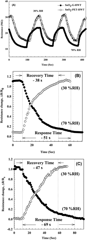 |
| | Fig. 10 (A) The resistance changes in the SnO2–G-HWT and SnO2–PET-HWT humidity sensor under three cycles of exposure to different % RH values from 30% to 70% at 20 ± 1 °C. (B) and (C) showed the humidity response (humidification from 30 to 70% RH) and recovery (desiccation from 70 to 30% RH) curves of SnO2–G-HWT and SnO2–PET-HWT humidity sensor at 20 ± 1 °C, respectively. | |
Table 1 Comparison of sensing properties of SnO2-based room temperature humidity sensors reported in literature
| Material |
Measurement range (% RH) |
Sensitivity |
Reference |
| SnO2–G-HWT |
5–95 |
0.36–0.97 [ΔR/R] |
This work |
| SnO2–PET-HWT |
|
0.24–0.72 [ΔR/R] |
| Fe–SnO2 |
0–100 |
0.8 [ΔR/R] |
4 |
| SFPG |
0–100 |
3.23 [ΔR/R] |
| SnO2–RGO |
11–97 |
0.15–0.45 [ΔR/R] |
36 |
| SnO2 |
5–95 |
0–0.98 [ΔR/R] |
37 |
4. Conclusions
In this research, transparent and crystalline SnO2 films were fabricated on non-seeded glass and directly deposited on a flexible PET substrate at a temperature below 100 °C. The HWT process did not only trigger the crystallization reaction of SnO2 but simultaneously induce the formation of hydroxyl species on the SnO2 surface, which led to an improvement of the conductivity of the as-prepared SnO2 films on both glass and PET substrates. The reaction mechanism of the HWT process was mainly based on the concept of typical water chemisorption and physisorption for ceramic type semiconductor sensing materials. Both the SnO2–G and SnO2–PET exhibited a dominant growth orientation along (110) according to the XRD results, which could form the stable configuration with dissociated water. The humidity sensing properties of both SnO2–G and SnO2–PET after the HWT process revealed an uptrend corresponding to the increase of the relative humidity, and the response/recovery time of SnO2–G-HWT and SnO2–PET-HWT exhibited 51/38 s and 69/47 s in the % RH range of 30–70% at 20 ± 1 °C of room temperature, respectively. The simple, low-temperature, and low-cost synthesis method of SnO2 reported in this study shows a good prospect for SnO2-based wearable electronic devices.
Conflicts of interest
There are no conflicts to declare.
Acknowledgements
This work was supported by a Grant-in-Aid for Scientific Research (B), 15H04122, of The Ministry of Education, Culture, Sports, Science and Technology (MEXT). A part of this work was also supported by Research Grant, The Murata Science Foundation. We thank Zoran Dinev, PhD, from Edanz Group (www.edanzediting.com/ac) for editing a draft of this manuscript.
References
- Z. M. Jarzebski and J. P. Marton, J. Electrochem. Soc., 1976, 123, 299c CrossRef.
- A. Azam, S. S. Habib, N. A. Salah and F. Ahmed, Int. J. Nanomed., 2013, 8, 3875 CrossRef PubMed.
- X. X. Lian, Y. Li, X. Q. Tong, Y. L. Zou, X. L. Liu, D. M. An and Q. Wang, Appl. Surf. Sci., 2017, 407, 447 CrossRef.
- D. Toloman, A. Popa, M. Stan, C. Socaci, A. R. Biris, G. Katona, F. Tudorache, I. Petrila and F. Iacomi, Appl. Surf. Sci., 2017, 402, 410 CrossRef.
- X. L. Xu, Y. Chen, G. H. Zhang, S. H. Yan, H. Q. Bian, Q. Chen, Y. Lu and S. Y. Ma, Mater. Lett., 2017, 195, 159 CrossRef.
- S. Nasresfahani, M. H. Sheikhi, M. Tohidi and A. Zarifkar, Mater. Res. Bull., 2017, 89, 161 CrossRef.
- X. Z. Wang, S. Qiu, J. R. Liu, C. Z. He, G. X. Lu and W. Liu, Eur. J. Inorg. Chem., 2014, 5, 863 CrossRef.
- S. H. Mohamed, J. Alloys Compd., 2011, 510, 119 CrossRef.
- S. Das and V. Jayaraman, Prog. Mater. Sci., 2014, 66, 112 CrossRef.
- L. Vayssieres and M. Graetzel, Angew. Chem., Int. Ed., 2004, 43, 3666 CrossRef PubMed.
- Y. C. Her, J. Y. Wu, Y. R. Lin and S. Y. Tsai, Appl. Phys. Lett., 2006, 89, 89 CrossRef.
- A. K. Subramani, N. Matsushita, T. Watanabe, M. Tada, M. Abe, K. Kondo and M. Yoshimura, Mater. Sci. Eng., B, 2008, 148, 136 CrossRef.
- H. Wagata, N. Ohashi, T. Taniguchi, A. K. Subramani, K. I. Katsumata, K. Okada and N. Matsushita, Cryst. Growth Des., 2010, 10, 3502 CrossRef.
- A. Lamberti, A. Chiodoni, N. Shahzad, S. Bianco, M. Quaglio and C. F. Pirri, Sci. Rep., 2015, 5, 7808 CrossRef PubMed.
- N. S. Saadi, L. B. Hassan and T. Karabacak, Sci. Rep., 2017, 7, 7158 CrossRef PubMed.
- K. Nose, A. Y. Suzuki, N. Oda, M. Kamiko and Y. Mitsuda, Appl. Phys. Lett., 2014, 104, 091905 CrossRef.
- V. Tomer and S. Duhan, Sens. Actuators, B, 2015, 220, 192 CrossRef.
- L. Greenspan, J. Res. Natl. Bur. Stand., Sect. A, 1977, 81A, 89 CrossRef.
- H. Cankurtaran, O. Yazici, S. Dinc and F. Karaman, Int. J. Electrochem. Sci., 2013, 8, 3265 Search PubMed.
- D. S. Madge, Entomol. Exp. Appl., 1961, 4, 143 CrossRef.
- D. Amalric-Popescu and F. Bozon-Verduraz, Catal. Today, 2001, 70, 139 CrossRef.
- J. A. Bonacin, R. R. Passos and L. A. Pocrifka, Mater. Res., 2015, 18, 639 CrossRef.
- S. H. Gordon, R. E. Harry-O'kuru and A. A. Mohamed, Talanta, 2017, 174, 587 CrossRef PubMed.
- H. Zhang, Y. Liu, K. Zhu, G. Siu, Y. Xiong and C. Xiong, J. Phys.: Condens. Matter, 1999, 10, 11121 CrossRef.
- P. Harrison and A. Guest, J. Chem. Soc., Faraday Trans., 1987, 83, 3383 RSC.
- R. Hu, J. Zhao and J. Zheng, Mater. Lett., 2017, 197, 59 CrossRef.
- B. Skariah, J. Naduvath and B. Thomas, Ceram. Int., 2015, 42, 7490 CrossRef.
- Z. Huang, L. Bi, Z. Zhang and Y. Han, Mol. Med. Rep., 2012, 6, 709 CrossRef PubMed.
- Y. Zhao, X. Song, Q. Song and Z. Yin, CrystEngComm, 2012, 14, 6710 RSC.
- J. Moulder, W. Stickle, P. Sobol and K. Bomben, Handbook of X-Ray Photoelectron Spectroscopy, Physical Electronics USA inc., Minnesota, 1995, 126 Search PubMed.
- H. Uchiyama, H. Ohgi and H. Imai, Cryst. Growth Des., 2006, 6, 2186 CrossRef.
- A. Mikhaylov, A. Medvedev, T. Tripol'skaya, V. Popov, A. Mokrushin, D. Krut'ko, P. Prikhodchenko and O. Lev, Dalton Trans., 2017, 46, 16171 RSC.
- S. Y. Tsai, Y. M. Lu, J. J. Lu and M. H. Hon, Surf. Coat. Technol., 2006, 200, 3241 CrossRef.
- Z. Chen and C. Lu, Sens. Lett., 2005, 3, 274 CrossRef.
- H. Farahani, R. Wagiran and M. Hamidon, Sensors, 2014, 14, 7881 CrossRef PubMed.
- D. Zhang, H. Chang and R. Liu, J. Electron. Mater., 2016, 45, 4275 CrossRef.
- M. Parthibavarman, V. Hariharan and C. Sekar, Mater. Sci. Eng., C, 2011, 31, 840 CrossRef.
|
| This journal is © The Royal Society of Chemistry 2018 |
Click here to see how this site uses Cookies. View our privacy policy here. 
 Open Access Article
 This Open Access Article is licensed under a Creative Commons Attribution-Non Commercial 3.0 Unported Licence
 a,
Yuta Katayanagib,
Tetsuo Kishia,
Tetsuji Yanoa and
Nobuhiro Matsushita*a
a,
Yuta Katayanagib,
Tetsuo Kishia,
Tetsuji Yanoa and
Nobuhiro Matsushita*a