
 Open Access Article
 This Open Access Article is licensed under a Creative Commons Attribution-Non Commercial 3.0 Unported Licence
Nanostructuring of Si substrates by a metal-assisted chemical etching and dewetting process
Andrzej Stafiniak *,
Joanna Prażmowska,
Wojciech Macherzyński and
Regina Paszkiewicz
*,
Joanna Prażmowska,
Wojciech Macherzyński and
Regina Paszkiewicz
Faculty of Microsystem Electronics and Photonics, Wroclaw University of Science and Technology, Janiszewskiego St. 11/17, 50-372 Wroclaw, Poland. E-mail: andrzej.stafiniak@pwr.edu.pl
First published on 5th September 2018
Abstract
In this work, we reported on the development of lithography-free technology for the fabrication of nanopatterned Si substrates. The combination of two phenomena, the solid-state dewetting process and metal-assisted wet chemical etching, allowed for fabrication of Si nanocolumns on large areas in a relatively simple way. The process of dewetting the thin metal layer enabled formation of nickel nanoislands, which were used as a shadow mask in the deposition of a catalytic metal pattern. Application of the two-stage dewetting process with the repetition of the metal deposition and annealing step enabled us to obtain a significant increase in the surface coverage ratio and the surface density of the nanoislands. As a catalytic metal, a gold layer was applied in the metal-assisted wet chemical etching process. The obtained columnar nanostructures showed a great verticality and had a high aspect ratio. In the conducted studies, the maximum etching rate (at RT) was higher than 1.2 μm min−1. The etching rate increased with increasing concentration of oxidizing (H2O2) and etching (HF) agent, with a tendency to saturate for more concentrated solutions. The etching rate was significantly higher for Si substrates with a crystallographic orientation (115) than for (111), but there was no privileged direction of etching except for the direction vertical to the substrate. With increasing layer thickness of the catalytic metal a decrease in the metal-assisted wet chemical etching process efficiency was observed. The developed technology allows for fabrication of patterned substrates with a wide range of lateral dimension of nanocolumns and their density.
Introduction
Nanostructuring of Si substrates is widely used in various applications to improve their efficiency, including in optoelectronic (photovoltaic cells, detectors, emitters) devices, electronic devices, gas and bio-sensors, and energy storage.1–7 There are two approaches to Si nanostructure fabrication: the top-down approach with wet or dry etching methods, and the bottom-up approach including methods of growth or deposition of nanostructures. The most commonly used method for patterning of silicon substrates is wet chemical etching of silicon in basic solutions (KOH, NaOH). However, this technique makes it difficult to obtain vertical patterns on the substrate, while using the dry methods the anisotropy of the structures could be easily obtained.An alternative method to the dry etching technique for producing Si structures with a high aspect ratio could be metal-assisted wet chemical etching (MaCE). The thin layer or nanoparticles of noble metals such as Au, Ag, Pt, or Au/Pd in MaCE catalysed the etching processes of Si in solution of hydrofluoric acid (HF) and an oxidizing agent like hydrogen peroxide (H2O2). The noble metals significantly accelerated the etching process and as a result, a “sinking” effect of the catalytic metal in the Si substrate could be observed. The surface of a catalytic metal can act as the cathode in the etching solution, which initiates the reduction reaction of H2O2 with electrons consumption. Then on the interface of catalytic metal and semiconductor, that works as the anode, Si oxidation process occurs with the release of electrons. This results in a difference of potential, and a local current flow occurs. Oxide is soluble in an acidic solution causing removal of semiconductor materials.8,9
The MaCE method shows high Si etching rates exceeding the 1.5 μm min−1, and enables an opportunity to fabricate a wide range of vertical structures, depending on the shape of the catalytic metal thin films or particles.10,11 Nanostructuring of Si substrates by the MaCE technique can be carried out using lithographic and non-lithographic methods. Lithographic methods are based on fabrication of desirable catalytic metal pattern.1,12 Non-lithographic methods use various ways to depose catalytic metal into the form of a discontinuous layer, islands7,8,10,13 or particles from a colloidal suspension.14–17 Density of particles, islands and cracks in a metal layer determines whether the obtained structures are more like porous material or nanowires. Other non-lithographic methods may include the use of sample preparation to fabricate a pattern that acts as a shadow mask before a catalytic layer deposition like self-organizing polystyrene spheres18–21 or imprinting technique.4
In this study, the solid-state dewetting (SSD) process of thin metal films for metal islands formation was applied. The Ni spherical islands were used for a pattern of holes in Au catalytic metal layer formation. Nickel was chosen because it undergoes SSD process and it can be removed relatively easily. For example, thin Al layers oxidize even at room temperature, which disable the SSD process. The combination of MaCE and SSD methods allowed us to form Si substrates with high aspect ratio nanocolumns. The aim of our research was to develop the lithography-free technology of fabrication of patterned Si substrates with wide range lateral dimension of nanocolumns and their density. It could be used for the metal–organic vapour phase epitaxial growth of GaN-based layers with enhanced quality for epitaxial lateral overgrowth method. Moreover, this type of structures could also be used in many different applications such as Li-ion battery anodes,22,23 enhanced light-emitting areas,4 ultra-low antireflection arrays.24
Experimental details
Sample preparation
In this study we used the p-type Si (111) and Si (115) substrates with resistivity of >500 Ω cm coated by 30 nm SiO2 using PECVD process were used. The substrates were cut into 12 × 12 mm2 samples. On the Si samples the 10 or 20 nm Ni layer were deposited with deposition rate of 0.5 Å s−1, by electron beam evaporation method using the PVD UHV system (K. J. Lesker, PVD 225). Then the samples, with Ni layers, were annealed at 850 °C in a rapid thermal annealing (RTA) system to activate the SSD process. The RTA processing was conducted in a nitrogen atmosphere for 5 min. Then, on a part of samples with 10 nm Ni layers the deposition of 10 or 20 nm Ni layers and RTA processing were repeated.Next the samples were etched in buffered hydrofluoric acid (BHF) solution, to remove SiO2 layer placed between Ni islands that acted as a mask in the etching process. Subsequently, the substrates were covered by Au catalytic metal layer, with deposition rate of 1 Å s−1, using evaporation method. Three thicknesses of catalytic metal layers 7, 10, 17 nm were examined. Then Ni islands were etched in ultrasonic bath of 10% HF solution by 1 min that caused the detachment of Au layer from the top of the islands. As a result, a holes pattern in the catalytic layer was obtained.
The 40% HF (VLSI, Technic France) water solution, 30% H2O2 (VLSI, Technic France) and DI water was used to prepare the MaCE etching solution. The etching processes were conducted at room temperature.
Characterization
We performed the scanning electron microscopy SEM (Hitachi, Su6600) characterization, to evaluate the surface topography of samples. To determine the size and surface distribution of the Ni islands from SEM images the tool for the particles characterization of the “ImageJ” software was used. This tool allows to define individual islands area (in pixels) and their quantity in the image, which permitted us to determine the islands radius, surface density and coverage ratio. Coverage ratio corresponds to the degree of samples surface coverage by the metal. Average values and standard deviation values of all parameters were then calculated from at least three SEM images taken for each sample. In order to determine the height of the obtained Si nanocolumns, the breakthroughs of the samples were made and the cross-sectional scans were obtained and analysed.Results and discussion
In Fig. 1 the technological process flowchart of nanostructuring of Si substrates are presented. The Si substrates were coated by a SiO2 layer to facilitate the SSD process of Ni layer. At elevated temperature nickel diffused interstitially into the Si substrate. The formation of Ni2Si or other intermetallic phases of nickel silicide on Ni/Si interface could occur.25 This intermetallic phases prevented lateral mass transport and creation of separated metal islands. Thin SiO2 layer, sub-10 nm, could inhibit the diffusion of Ni atoms to Si substrate and formation of silicide alloy, which enabled initiation of the SSD process.26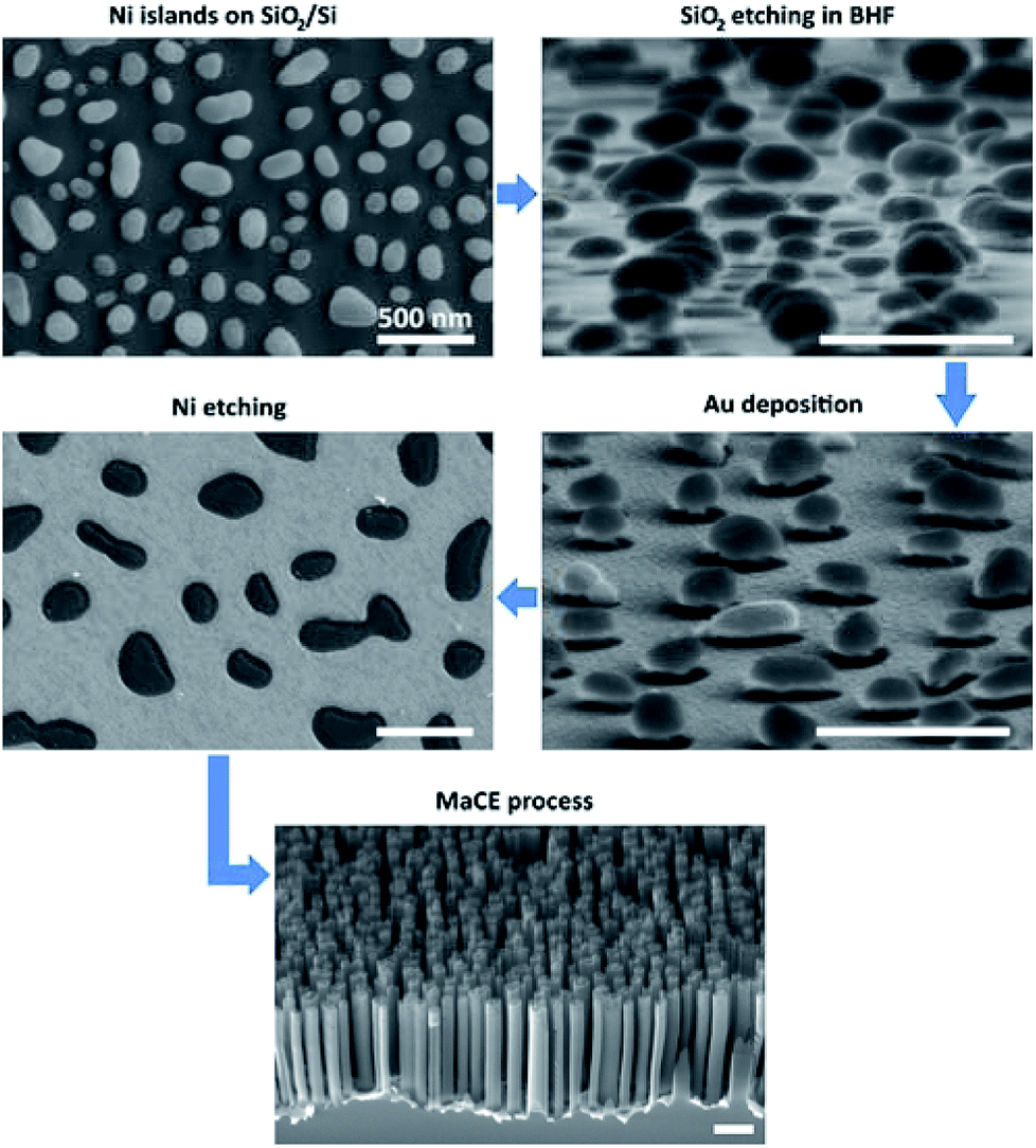 | ||
| Fig. 1 Technological process flowchart of Si substrates nanostructurization, following stages: solid-state dewetting of Ni layer, etching of SiO2 layer in BHF solution, deposition of Au layer, etching of Ni islands in HF solution, MaCE process of Si substrate. Scale bar – 500 nm. | ||
In our case we have proposed a thicker oxide layer – 30 nm – which acted as a spacer between Ni island and Si substrate in the next technological step. After SiO2 etching, the mushroom like structures from metal islands and SiO2 spacer were obtained. On these structures the catalytic metal layer was deposited. The discontinuity of the Au layer was observed at the edge of the islands (Fig. 1). This allowed us to remove Ni islands with a part of the Au layer in HF solution, in the same procedure as in the lift-off method, where Ni acts as a photoresist. The resulting holes pattern in the Au layer was a negative image of the islands shape (Fig. 1).
In Fig. 2 the SEM images of Si substrate with 10 nm, 10 nm + 10 nm, 10 nm + 20 nm, 20 nm Ni layer after annealing at 850 °C are presented. After thermal activation, the effect of SSD mechanism was clearly visible and separated islands were obtained. To determine the size and surface distribution of the Ni islands from SEM images, the “ImageJ” software was used. By assuming the idealized spherical shape of the islands, their radiuses were determined and the histograms of the radius values are presented in Fig. 2. Table 1 shows the results of samples topography analysis after annealing process, the values of the islands area, radius, surface density and coverage ratio.
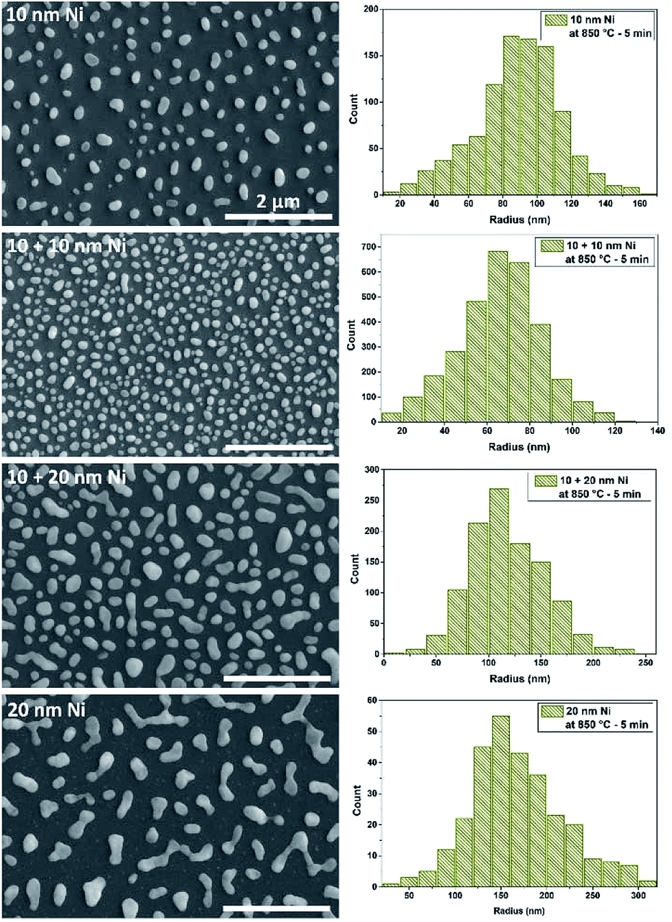 | ||
| Fig. 2 SEM images of the 10 nm, 10 nm + 10 nm, 10 nm + 20 nm and 20 nm Ni layers on SiO2/Si substrates annealed at 850 °C temperature and the histograms of Ni islands radius. Scale bar – 2 μm. | ||
| Ni thickness (nm) | Area (10−3 μm2) | Radius (nm) | Density (μm−2) | Coverage (%) |
|---|---|---|---|---|
| 10 nm | 26.5 ± 13.2 | 91.8 | 6.3 ± 0.4 | 16.5 |
| 10 + 10 nm | 14.9 ± 8.0 | 68.9 | 20.8 ± 1.9 | 30.7 |
| 10 + 20 nm | 47.3 ± 28.6 | 122.7 | 7.2 ± 0.6 | 33.8 |
| 20 nm | 99.7 ± 69.0 | 178.0 | 2.2 ± 0.05 | 21.6 |
Comparing the SSD process of 10 nm and 20 nm Ni layers, the mechanism of self-organization into isolated spherical islands occurred quicker for the thinner layer. In case of 20 nm thick Ni layers the islands had irregular shape and they were not fully separated. The average value of the Ni islands radius for 10 nm layers was 91.8 nm and surface density was 6.3 μm−2, for 20 nm layers radius – 178 nm and surface density – 2.2 μm−2. These values were similar, slightly smaller, than the values obtained by another group under similar conditions.26 In general, for thicker metal layers the islands size increased and the surface density decreased. These parameters can be controlled also by the RTA process conditions, like temperature or annealing time. The higher coverage ratio for thicker metal layer, 21.6% (20 nm Ni) compared to 16.5% (10 nm), is associated with that the islands were not fully formed in quasi-ideal sphere. However the coverage ratio usually did not exceed 25% for fully formed islands.27
To obtain a higher coverage ratio at comparable Ni islands surface densities, the deposition of metal layer and the SSD process should be repeated.28 To repeat this step, we tried two thicknesses of the Ni layer: 10 nm and 20 nm. The metal layers were deposited on samples with the nanoislands obtained from the dewetting process of 10 nm Ni layer. In case of samples with the repeated process of 10 nm + 10 nm thick Ni layer the average value of radius and surface density of the islands were respectively 68.9 nm and 20.8 μm−2 and coverage ratio was 30.7%. Comparing these values to the islands obtained from a single 10 nm Ni layer, the islands size slightly decreased, the density increased several times and the coverage ratio was almost doubled. In the case of samples with repeated process of 10 + 20 nm Ni layer the average value of radius increased to 122.7 nm, the surface density was on a level similar to the single 10 nm Ni layer (7.2 μm−2) and the coverage ratio was 33.8%. In both situations, nearly two-fold increase in coverage ratio was obtained, but in case of 10 nm + 10 nm Ni layer the surface density of the islands was significantly higher. This is probably due to the fact that the second 10 nm metal layer was too thin to be continuous on the islands borders. Breaks in the metal layer initiated the formation of new, smaller islands between the existing ones, therefore, the average radius value decreased to 68.9 nm.
In the next step, the thin layer of silicon oxide (30 nm) was etched in BHF solution to expose the Si surface. The resulting mushroom-like structures allowed to form a hole pattern in the Au catalytic layer. Such prepared samples were used to study of the MaCE process and the possibility of nanostructuring of Si substrates.
For an experiment, five water solutions of different concentrations of HF and H2O2 were prepared to check the impact of the oxidizing and reducing agent on MaCE: 20% HF/2.5% H2O2 (10 M/0.69 M), 10% HF/2.5% H2O2 (5 M/0.69 M), 5% HF/2.5% H2O2 (2.5 M/0.69 M), 10% HF/5% H2O2 (5 M/1.39 M), 10% HF/0.3% H2O2 (5 M/0.08 M). The samples were immersed in etching solutions for 5 min. In Fig. 3 the SEM cross-section images of the effect of the metal-assisted wet chemical etching of Si (111) and (115) substrates in the aforementioned solutions and with 10 nm Au layer are presented. Thanks to the pattern of holes in the catalytic metal layer, the columnar nanostructures were obtained.
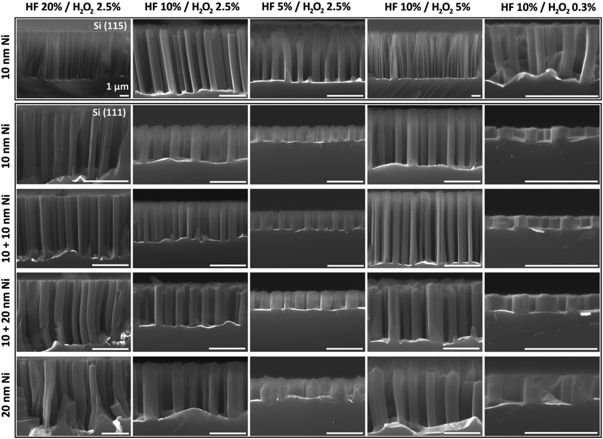 | ||
| Fig. 3 SEM images of the effect of the metal-assisted wet chemical etching of Si (111) and Si (115) substrates in solutions with different HF and H2O2 concentrations. Thickness of Au layer was 10 nm. Scale bar – 1 μm. | ||
From the cross-section images, the heights of etched structures were determined. This allowed to calculation of the average etching rate values for each solution and substrates which were collected in Table 2 (change of HF concentration) and Table 3 (effect of H2O2 concentration). In Fig. 4 the comparison of dependence of MaCE etching rate of Si (111) and Si (115) for different density distribution of hole pattern in Au layer on HF and H2O2 concentrations is presented. Both in the range of changing the HF (Fig. 4a) and H2O2 (Fig. 4b) concentration, the etching rate increased with increasing concentration of oxidizing and etching agent, with a tendency to saturate for more concentrated solutions. This behavior is natural, but with the constantly increasing concentration of one reagent, in case of large differences in the concentration between HF and H2O2, we should observe the maximum of etching rate.23,29
| HF (%) | Etching rate (μm min−1) | ||||
|---|---|---|---|---|---|
| 10 nm Ni/Si (115) | 10 nm Ni/Si (111) | 10 + 10 nm Ni/Si (111) | 10 + 20 nm Ni/Si (111) | 20 nm Ni/Si (111) | |
| 5 | 0.32 ± 0.01 | 0.086 ± 0.01 | 0.11 ± 0.01 | 0.1 ± 0.01 | 0.095 ± 0.01 |
| 10 | 0.55 ± 0.04 | 0.24 ± 0.01 | 0.25 ± 0.02 | 0.25 ± 0.02 | 0.29 ± 0.02 |
| 20 | 1.21 ± 0.1 | 0.42 ± 0.03 | 0.41 ± 0.03 | 0.39 ± 0.04 | 0.46 ± 0.05 |
| H2O2 (%) | Etching rate (μm min−1) | ||||
|---|---|---|---|---|---|
| 10 nm Ni/Si (115) | 10 nm Ni/Si (111) | 10 + 10 nm Ni/Si (111) | 10 + 20 nm Ni/Si (111) | 20 nm Ni/Si (111) | |
| 0.3 | 0.15 ± 0.01 | 0.046 ± 0.004 | 0.041 ± 0.003 | 0.055 ± 0.005 | 0.07 ± 0.008 |
| 2.5 | 0.55 ± 0.04 | 0.24 ± 0.01 | 0.25 ± 0.02 | 0.25 ± 0.02 | 0.29 ± 0.02 |
| 5 | 0.96 ± 0.06 | 0.38 ± 0.04 | 0.4 ± 0.02 | 0.35 ± 0.02 | 0.34 ± 0.04 |
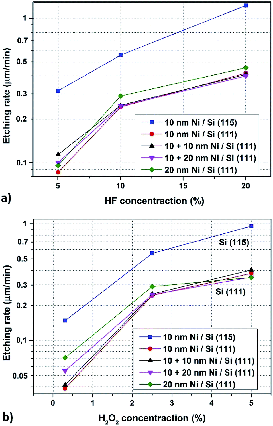 | ||
| Fig. 4 The dependence of etching rate of Si (111) and Si (115) substrates on HF concentration in the MaCE process, concentration of H2O2 – 2.5% (a); the dependence of etching rate of Si (111) and Si (115) substrates on H2O2 concentration in MaCE process, concentration of HF – 10% (b). | ||
The obtained etching rates are similar to literature values ranging from several hundreds of nm min−1 to single of μm min−1 in comparable concentrations of etching agents and at room temperature.10,12 However, it is difficult to refer directly to the rate values because there are many parameters (beyond easy to define as substrate doping and orientation or type and thickness of catalytic metal) like size and shape of catalytic metal pattern, layers, discontinuous layers, nanoparticles, density of metal structures or spacing that should be included.30
Samples based on Si substrates with (115) orientation had the highest etching rate after immersion in the prepared solution. This is probably due to the fact that the (115) plane has a lower density of atoms compared to (111) plane. The situation is similar as in the case of conventional wet etching where the substrate with (111) orientation had the lowest etching rate because of the higher coordination of silicon atoms in (111) surfaces.31
Probable models describing the MaCE mechanism assume the possibility of two phenomena: (1) the reagent and product of etching process diffuse along the interface between the catalytic metal and the Si substrate, (2) dissolution of Si atoms in catalytic metal and their diffusion through the metal to the surface and then their oxidation and etching in agents.8 In the first case the influence of the surface area of the catalytic metal, or rather the characteristic size (minimal length between edges of the metal template), should be significant for the value of the etching rate. Rykaczewski et al. experimentally showed this dependence in their studies where for the decreasing characteristic length the efficiency of etching increase.30 Accordingly, in our research the etching rate should be the highest for samples with Au pattern for substrates covered by 10 nm + 10 nm and 10 nm + 20 nm Ni layer, because in these situations the Ni islands are closest to each other. However, such dependence was not observed in our research, the values of the etching rate were comparable and within the error limits. In addition, samples covered by 20 nm Ni layer, i.e. the substrate with the largest distance between Ni islands, had a slightly higher etching rate. This was probably because of better removal of reaction products.
No influence of the Au pattern density suggests that in our case the second model of MaCE etching dominates, i.e. diffusion through the catalytic metal. It is even more probable considering the thickness of the Au layer, where in our case it was 10 nm (comparing to Rykaczewski's research – 50 nm). In Fig. 5 the dependence of MaCE etching rate of Si (115) substrates on Au layer thickness from 7 to 17 nm are presented. Approximating this dependence for Au layer thickness up to 50 nm, the value of etching rate would be reduced by several times.
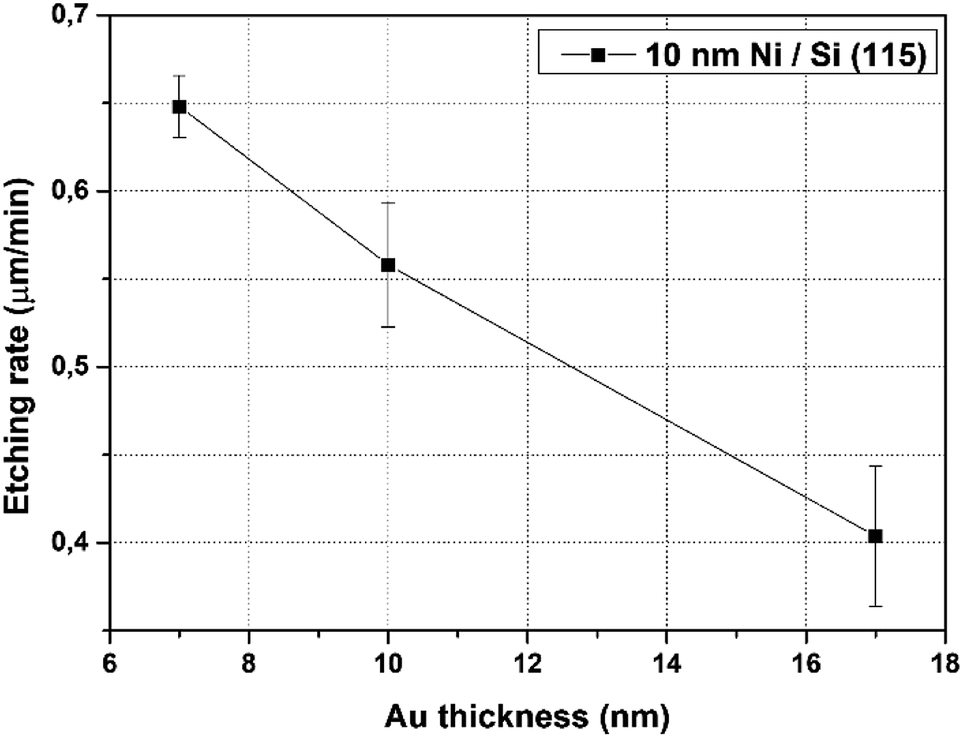 | ||
| Fig. 5 The dependence of etching rate of Si (115) substrates on Au layer thickness in MaCE process (10 nm Ni), concentration of HF – 10%, H2O2 – 2.5%, etching time 5 min. | ||
For the smallest concentrations of each of the etching agents a large dispersion of the etching rate depending on the density of the catalytic metal pattern was observed. This can be caused by inhomogeneous and insufficient supply of reagents to the etched surface.
In the experiment, mostly straight and vertical Si nanocolumns were obtained. Only in one case, non-vertical structures homogeneously inclined at an angle of 9.2° ± 0.7° on the entire sample were observed for Si (115) and ratio of etching factors 10% HF/2.5% H2O2. This angle gives the 〈113〉 direction of etching structures.
Change of the ratio of HF to H2O2 concentration could have impact on etching direction and surface morphology of Si nanocolumns. In general, for (111) substrates the low concentration of oxidant factors leads to a change of etching direction from vertical to 〈100〉 crystallographic direction.16 However, choosing the right concentration levels and ratios to obtain inclined structures is not obvious because the MaCE process is more complex and more factors affect, such as process temperature, oxidant type or catalytic metal.4,16,32 Furthermore, to control the shape and direction of obtained structures organic additives are used in etching solutions.14,16 In our case, the etching conditions were the same throughout the process. Twisted structures at the base (Fig. 1) could be caused by a low concentration of the oxidizing agent (due to the lack of effective mixing of the solution) or as a result of different etching rate of the catalytic layer resulting from local narrowing.
For structures fabricated in a solution with a low HF/H2O2 ratio, i.e. with a relatively high content of oxidizing agent, gentle porosity of the columns could be observed, in particular top part of structures. This occurs when there is an excessive number of holes generated on the cathode, where the reduction reactions of oxidant are catalyzed. Then the holes are injected to metal–semiconductor interface where they are involved in the oxidation process. Some of them can diffuse into the semiconductor causing porosity of the surface.33,34
Conclusions
In this work, we reported on the development of a lithography-free technology for fabrication of nanopatterned Si substrates. The combination of two phenomena, the solid-state dewetting process and the metal-assisted wet chemical etching allowed to fabrication of large areas with nanocolumns in a simple way.The two-stage process with the repetition of the SSD step enables for a nearly two-fold increase in the surface coverage ratio by Ni islands, in one case (10 + 10 nm Ni) by significantly increasing the surface density, in the other case (10 + 20 nm Ni) by increasing the size of the islands while maintaining a similar density.
Nanostructures fabricated by MaCE process showed a good verticality and had a high aspect ratio. In the conducted studies, the maximum etching rate was higher than 1.2 μm min−1. The etching rate increased with increasing concentration of the oxidizing (H2O2) and the etching (HF) agent, with a tendency to saturate for more concentrated solutions. Etching rate was significantly higher for substrates with a crystallographic orientation of Si (115), but there was no privileged direction of etching beyond the vertical to the substrate. No significant differences in the etching rate depending on the density or narrowing of the catalytic metal pattern were observed. This suggested that diffusion through the catalytic metal dominated in our MaCE processes. This was confirmed by the dependence of the etching rate on the thickness of the catalytic layer i.e. decreasing layer thickness of the catalytic metal, increased the MaCE process efficiency.
Future research will focuse on the optimization of parameters such as height, diameter and density of nanocolumns for fabrication of Si wafer templates that could be used for the epitaxial lateral overgrowth (ELO) method for deposition of GaN-based structures of enhanced quality.
Conflicts of interest
There are no conflicts to declare.Acknowledgements
This work was co-financed by the National Centre for Research and Development grants TECHMASTRATEG No. 1/346922/4/NCBR/2017 and LIDER No. 027/533/L-5/13/NCBR/2014, the National Science Centre grant No. DEC-2015/19/B/ST7/02494, Wroclaw University of Technology statutory grants and by the Slovak-Polish International Cooperation Program. This work was accomplished thanks to the product indicators and result indicators achieved within the projects co-financed by the European Union within the European Regional Development Fund, through a grant from the Innovative Economy (POIG.01.01.02-00-008/08-05) and by the National Centre for Research and Development through the Applied Research Program Grant No. 178782.Notes and references
- N. Singh, K. D. Buddharaju, S. K. Manhas, A. Agarwal, S. C. Rustagi, G. Q. Lo, N. Balasubramanian and D.-L. Kwong, IEEE Trans. Electron Devices, 2008, 55, 3107–3118 Search PubMed.
- H. Wu and Y. Cui, Nano Today, 2012, 7, 414–429 CrossRef.
- O. L. Muskens, J. Gómez Rivas, R. E. Algra, E. P. A. M. Bakkers and A. Lagendijk, Nano Lett., 2008, 8, 2638–2642 CrossRef PubMed.
- W. Chern, K. Hsu, I. Su Chun, B. P. de Azeredo, N. Ahmed, K.-H. Kim, J. Zuo, N. Fang, P. Ferreira and X. Li, Nano Lett., 2010, 10, 1582–1588 CrossRef PubMed.
- X. Geng, Z. Qi, M. Li, B. K. Duan, L. Zhao and P. W. Bohnb, Sol. Energy Mater. Sol. Cells, 2012, 103, 98–107 CrossRef.
- Y. Li, M. Li, D. Song, H. Liu, B. Jiang, F. Bai and L. Chu, Nano Energy, 2015, 11, 756–764 CrossRef.
- B. Jiang, M. Li, Y. Liang, B. Yang, D. Song, Y. Lia and J. Luo, Nanoscale, 2016, 8, 3085–3092 RSC.
- Z. Huang, N. Geyer, P. Werner, J. de Boor and U. Gösele, Adv. Mater., 2011, 23, 285–308 CrossRef PubMed.
- X. Li, Curr. Opin. Solid State Mater. Sci., 2012, 16, 71–81 CrossRef.
- J. Teva, Z. J. Davis and O. Hansen, J. Micromech. Microeng., 2010, 20, 015034 CrossRef.
- H. Han, Z. Huang and W. Lee, Nano Today, 2014, 9, 271–304 CrossRef.
- K. Rykaczewski, O. J. Hildreth, D. Kulkarni, M. R. Henry, S.-K. Kim, C. P. Wong, V. V. Tsukruk and A. G. Fedorov, ACS Appl. Mater. Interfaces, 2010, 2, 969–973 CrossRef PubMed.
- J. J. Patil, B. D. Smith and J. C. Grossman, RSC Adv., 2017, 7, 11537 RSC.
- M.-L. Zhang, K.-Q. Peng, X. Fan, J.-S. Jie, R.-Q. Zhang, S.-T. Lee and N.-B. Wong, J. Phys. Chem. C, 2008, 112, 4444–4450 CrossRef.
- C.-Y. Chen, C.-S. Wu, C.-J. Chou and T.-J. Yen, Adv. Mater., 2008, 20, 3811–3815 CrossRef.
- Z. Huang, T. Shimizu, S. Senz, Z. Zhang, N. Geyer and U. Gosele, J. Phys. Chem. C, 2010, 114, 10683–10690 CrossRef.
- R. Li, M. Li, Y. Li, P. Fu, Y. Luo, R. Huang, D. Song and J. M. Mbengue, RSC Adv., 2015, 5, 96483–96487 RSC.
- Y. Chen, L. Li, C. Zhang, C.-C. Tuan, X. Chen, J. Gao and C.-P. Wong, Nano Lett., 2017, 17, 1014–1019 CrossRef PubMed.
- B. Zhou, X. Li, T. Shi, G. Liu, H. Cao and Y. Wang, J. Mater. Sci., 2017, 52, 6449–6458 CrossRef.
- F. Teng, N. Li, D. Xu, D. Xiao, X. Yang and N. Lu, Nanoscale, 2017, 9, 449 RSC.
- H. Cao, X. Li, B. Zhou, T. Chen, T. Shi, J. Zheng, G. Liu and Y. Wang, Nanoscale Res. Lett., 2017, 12, 105 CrossRef PubMed.
- S. Chang, J. Oh, S. T. Boles and C. V. Thompson, Appl. Phys. Lett., 2010, 96, 153108 CrossRef.
- W. McSweeney, H. Geaney and C. O'Dwyer, Nano Res., 2015, 8, 1395–1442 CrossRef.
- C. Zhang, S. Li, W. Ma, Z. Ding, X. Wan, J. Yang, Z. Chen, Y. Zou and J. Qiu, J. Mater. Sci.: Mater. Electron., 2017, 28, 8510–8518 CrossRef.
- A. M. Thron, P. K. Greene, K. Liu and K. van Benthem, Acta Mater., 2012, 60, 2668–2678 CrossRef.
- P.-H. Lee and C.-C. Chang, Surf. Sci., 2007, 601, 362–375 CrossRef.
- A. Stafiniak, T. Szymański and R. Paszkiewicz, Appl. Surf. Sci., 2017, 426, 123–132 CrossRef.
- M. Kang, S. G. Park and K. H. Jeong, Sci. Rep., 2015, 5, 14790 CrossRef PubMed.
- C. Chartier, S. Bastide and C. Lévy-Clément, Electrochim. Acta, 2008, 53, 5509–5516 CrossRef.
- K. Rykaczewski, O. J. Hildreth, C. P. Wong, A. G. Fedorov and J. H. J. Scott, Nano Lett., 2011, 11, 2369–2374 CrossRef PubMed.
- M. A. Gosálvez, I. Zubel and E. Viinikka, Chapter Twenty Four – Wet Etching of Silicon, in Micro and Nano Technologies, William Andrew Publishing, Boston, 2010 Search PubMed.
- H. Chen, H. Wang, X.-H. Zhang, C.-S. Lee and S.-T. Lee, Nano Lett., 2010, 10, 864–868 CrossRef PubMed.
- K. Tsujino and M. Matsumura, Electrochim. Acta, 2007, 53, 28–34 CrossRef.
- D. H. Lee, Y. Kim, G. S. Doerk, I. Laboriante and R. Maboudian, J. Mater. Chem., 2011, 21, 10359 RSC.
| This journal is © The Royal Society of Chemistry 2018 |