
 Open Access Article
 This Open Access Article is licensed under a Creative Commons Attribution-Non Commercial 3.0 Unported Licence
Optimized inkjet-printed silver nanoparticle films: theoretical and experimental investigations†
Sreemannarayana Mypati,
Shankar R. Dhanushkodi ,
Michael McLaren,
Aristides Docoslis,
Brant A. Peppley and
Dominik P. J. Barz*
,
Michael McLaren,
Aristides Docoslis,
Brant A. Peppley and
Dominik P. J. Barz*
Department of Chemical Engineering, Queen's University, Kingston, ON K7L 3N6, Canada. E-mail: dominik.barz@queensu.ca; Fax: +1 613 5336637; Tel: +1 613 5336000 ext. 79470
First published on 29th May 2018
Abstract
We study the influence of inkjet printing scheme and sintering parameter on the electrical resistivity of multi-layer silver nanoparticle films. A central composite Design Of Experiments (DOE) is employed to maximize experimental efficiency and improve the statistical significance of parameter estimates. The resulting mathematical correlations allow to interpret the influence of the print and sintering parameters. Detailed inspection of the correlations reveals the existence of local extrema and indicates that a structured approach such as the DOE would be significantly more effective for fabricating films with a minimum of resistivity. Furthermore, we modify the well-known Fuchs–Sondheimer Mayadas–Shatzkes model to correlate the resistivity of a multi-layer nanoparticle film with the sintering temperature and time. The modified model uses literature data but one constant inferred from two experiments. After model adjustment, the resistivities of films fabricated with different parameters can be predicted with good accuracy. This validation tremendously increases applicability and relevance of the model.
1 Introduction
In the last decade, inkjet printing became a versatile technology and is used for various applications such as printable/stretchable electronics,1–3 batteries,4 electrochromic devices,5 optoelectronics6 and sensors.7–9 Inkjet printing is a digital printing method which allows for rapid material deposition with the ability for non-contact, maskless and additive patterning. The advantages are, amongst others, low cost, reduced material waste, and scalability for large area manufacturing while the produced layers are uniform, well dispersed and with fewer morphological defects.10 Several reviews on material inks and inkjet printing are available, cf. Singh et al.,11 Yang et al.12 and Choi et al.13For many inkjet applications, one of the most important tasks is the deposition of electrically-conducting materials. The performance of printed conducting polymers is often not sufficient for high-quality (high-speed) electronics or large-area printing.14 Metal based inks offer significant advantages in terms of conductivity with ranges from 104 to 105 S cm−1 and metals of choice usually include silver, gold, copper and aluminium.15 These metals also have good operational stability, but regular manufacturing processes often require very high (sintering) temperatures and/or vacuum deposition.16 Nevertheless, alternative processes which prevent these unfavorable conditions were proposed in literature. For example, Shirai et al. prepared polyvinylpyrrolidone stabilized Tin nanoparticle inks that were printed and sintered at room temperature resulting in conductive films.17 Recently, intense pulsed light, also referred to as flash lamp annealing,18 has gained interest for sintering of nanomaterials since no further heat treatment is required.19 Likewise, it is possible to print a self-heatable conductive ink (Ag2O and silver 2,2-dimethyloctanoate) which does not require a costly external heating instrument for rapid sintering since the ink itself is capable of generating heat as high as 312 °C when its exothermic reaction is triggered at a temperature of 180 °C.20 Another approach involves printing of diethanolamine (DEA)-silver ammonia mixtures which decompose at temperatures higher than 50 °C and then form silver thin films.21
A very attractive strategy is to use metals that are dispersed in the form of nano-sized particles (NPs) since their sintering temperature is considerably lower and they are also suitable for inkjet printing. The utilization of inks made of silver nanoparticles (AgNPs) is especially advantageous because they disperse at high concentrations in environmentally friendly solvents such as water. Furthermore, they have much lower melting temperatures than bulk silver (962 °C) and show reasonable conductivities (resistivities) at sintering temperatures as low as 150 °C and can match the conductivity of gold NPs at lower costs.16,22 Here, several interesting alternatives to the regular thermal annealing can be found in literature. Öhlund et al. used an active coating to assist the sintering of inkjet printed silver nanoparticles on a paper.23 Olkkonen et al. sintered printed silver films in brine at 110 °C and observed electrical resistivities only two times higher than the bulk silver value.24 Vaithilingam et al.25 used infrared light for AgNPs sintering where the resulting surface temperature was in the range of 140 °C to 160 °C. Li et al. applied a xenon flash lamp to improve the properties of silver nano-plates during sintering at 180 °C.26 Even AgNPs sintering at room temperature was demonstrated by Magdassi et al. who used a countercharged polyelectrolyte to trigger a spontaneous coalescence without additional heating.27
To obtain high electrical conductivity and strong adhesion to the substrate, multiple layers of the AgNPs can be printed on top of each other. Sintering can be done in-between the printing of each layer but it is not obvious whether it is beneficial to sinter after each layer is printed or only for selected layers.
A schematic of the multi-particle sintering mechanisms is given in Fig. 1. Directly after printing, the particles are still surrounded by the solvent which slowly evaporates as indicated in the left part of Fig. 1. Over time or with increasing temperature, the solvent evaporates and the NPs establish contact with neighboring particle. At sufficient sintering temperatures, the interfacial energy between the particles decreases and the so-called neck growth occurs based on different diffusion mechanisms.28 The neck formation is initially triggered by surface diffusion which does not change the center-to-center distance of the particles. Hence, there is no densification of the layers at the beginning of sintering.29 During advanced stages of sintering, diffusion along the grain boundaries takes place where the centers of the particles come closer which increases the contact area;29,30 cf. the right part of Fig. 1. At the same time, matter moves from the particle bulk to the metal-pore interface. This decreases the pore surface area while the grain boundary area of the layers increases.31 The parameters of the NP sintering process are temperature and time. The grain size, density and consolidation of multiple-printed layers after sintering affect the film conductivity and depend on the variables of both printing and sintering process.30 Some insights in AgNPs sintering are available in the work of Stewart et al.32 who investigated the influence of temperature and particle shape on the film resistivity. However these films were neither printed nor was the influence of sintering time or film thickness investigated.
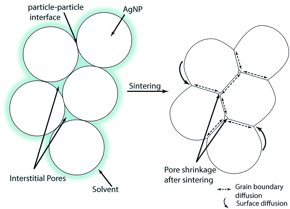 | ||
| Fig. 1 Illustration of multi-particle sintering mechanisms. | ||
Consequently, there is essentially no literature available that is concerned with the study of the thermal sintering (furnace) parameters of NP films consisting of multiple-printed layers. Likewise, no theoretical model exists that is able to quantify the resistivity of such manufactured films. The existing models for film resistivity are applicable if the manufacturing process does not require any thermal treatment over longer times, for example in case of physical vapor deposition. Despite the progress in low temperature sintering of nanoparticle films, as discussed above, we choose conventional thermal sintering using a furnace in this work. This method is cost-effective and does not require complex equipment or additives and is usually readily available. Hence, the main objectives of the present study are to: (i) investigate the influence of printing and sintering parameters on film resistivity in order to optimize the production of multiple-printed AgNP films with low electrical resistance; and (ii) develop a new modelling approach which correlates the influence of the sintering temperature and time on the resistivity of such-produced films. For the first part, we utilize a Design Of Experiment (DOE) method in order to identify the relationship between parameters associated with the (printing) process;33 we are not aware of any study in the literature that is based on such a structured and comprehensive approach.
This article continues with a section on the Experimental materials and methods followed by the derivation the model. Then, we plan the DOE and discuss the results. The experiments required for the DOE also serve for the validation of the model. Finally, the article is summarized with some concluding remarks.
2 Experimental materials and methods
In this section, we specify the materials, fabrication of the multi-layers films, and characterization techniques that are used in this study.2.1 Materials
A commercial AgNP ink (Metalon®JS-B40G, Novacentrix, Austin, TX, USA) is used in this study. The NPs size, pH and surface tension of the ink are measured with a dynamic light scattering technique (Zetasizer Nano ZS, Malvern Instruments Ltd, Malvern, UK), an electrochemical method (Sevenmulti™, Mettler Toledo, ON, Canada) and a pedant drop method (OCA25, DataPhysics Instruments GmbH, Filderstadt, Germany), respectively. The composition and properties of the ink are given in Table 1. Glass microscope slides with dimensions 75 × 25 × 1 mm3 (Fisher Scientific, Ottawa, ON, Canada) are used as the print substrate. Acetone and ethanol (reagent grade, Sigma-Aldrich Canada Company, Oakville, ON, Canada) are used for cleaning purposes.| Material properties | |
|---|---|
| Viscosity/mPa s | 6.8 ± 0.7 |
| Nano-particle size/nm | ![[thin space (1/6-em)]](https://www.rsc.org/images/entities/char_2009.gif) 50 ± 10 50 ± 10 |
| pH of the ink/— | 7 ± 0.3 |
| Surface tension/N m−1 | 0.03 ± 0.001 |
| Specific gravity/— | 1.56 |
2.2 Printing and sintering
At first, the glass substrates are thoroughly rinsed with ethanol and deionized water. The AgNP ink is printed on the glass substrates using a Dimatix Materials Printer (Model DMP-2800, FUJIFILM Dimatix Inc., Santa Clara, CA, USA). The appearance of the printed layers depends on the droplet-to-droplet spacing and the droplet size controlled by the firing voltage of the inkjet head. Furthermore, the distance of inkjet head to the substrate, viscosity and interfacial tension of the ink as well as the surface energy on the substrate are important. In this work, we consistently use a print droplet velocity of 10 m s−1 and a spacing of 25 μm on the glass substrates to ensure a uniform distribution of the ink.The film fabrication process is sketched in Fig. 2. Generally, the process consists of a sequence of printing (p) and sintering (s) of multiple layers. The printed samples are thermally sintered in a high-temperature box furnace at ambient pressure (ST-1200°-678, Sentro Tech Corp, Strongsville, OH, USA) whereas the optimal sintering temperature and time are unknown. The film fabrication process has two further degrees of freedom: (i) the number of printed layers; and (ii) the number of sintered layers. A natural question arises: is it useful – depending on the objective – to sinter every printed layer (p–s–p–s…) or only every i-th layer (p–p–s–p–p–s…)? Improvement of such a two-step, multiple factor process cannot be done by optimizing one parameter without the consideration of the others. That is, the parameters of the film fabrication process have to be simultaneously optimized; hence a multivariable optimization strategy is required.
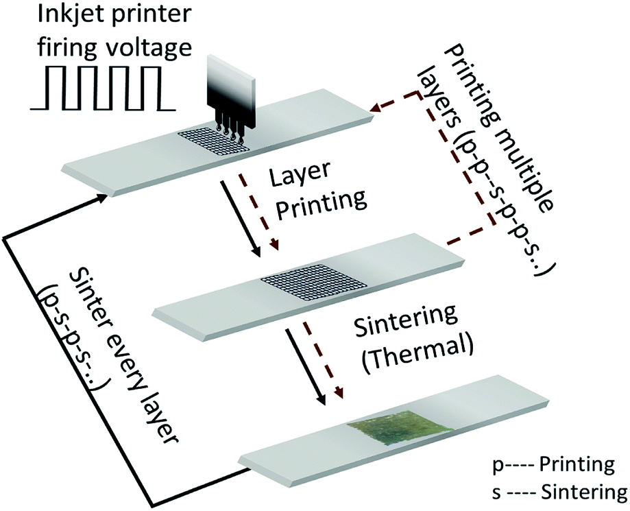 | ||
| Fig. 2 Schematic of inkjet printing and sintering of AgNP layers. Solid lines indicate the single layer printing and sintering scheme. Dashed lines indicate the multi-layer printing and sintering scheme. | ||
2.3 Film characterization
Insights into the morphology of the sintered films are obtained by taking images with a Scanning Electron Microscope (FEG MLA 650, FEI, Hillsboro, OR, USA) having a 1 μm resolution at a working distance of 10.3 mm. These SEM images are processed with the software ImageJ (Version: 1.50i, U.S. National Institutes of Health, Md, USA) to evaluate size and shape of the NP grains. The elemental composition of the thin film surface is obtained by the Energy-dispersive X-ray spectroscopy (FEG MLA 650, FEI, Hillsboro, OR, USA). The electric sheet resistance of the films is measured based on the van der Pauw method34 using a four-point probe station (S-1160, Signatone Corporation, Gilroy, CA, USA) equipped with four S-926 micropositioners along with two digital multimeters and a DC power supply (Multimeter Model: 34401A, Power Source U8002A, Agilent Technologies, Inc., Santa Clara, CA, USA). Film thickness is measured with a profilometer (DektakXT® stylus profiler, Bruker Corporation, Billerica, MA, USA). Finally, the resistivity ρ of the films is determined using the measured sheet resistance Rs and the film thickness d according to ρ = Rsd. All resistivity results reported in this article are averages that are based on at least six measurements. The standard deviation is always less than 5% of the average value.2.4 Design of Experiments
A common problem in multivariate analysis is the fact that initially it is not obvious which parameters have a significant influence on the desired output of a process. What is a suitable range for each parameter and are there strong interactions between parameters? Furthermore, it is generally not possible to optimize a single parameter without paying attention to the other criteria or constraints. Hence, the optimization of technical processes is cumbersome and requires a large set of experiments even for a very limited number of parameters. Design of experiments (DOE) is a systematic method to infer the relationship between parameters and the desired output. Its application allows for a reduced number of experiments while maintaining a high level of statistical significance.33 To evaluate the factors that influence the AgNP film resistivity, a two level-three factor central composite design (CCD) is performed using the statistics software MINITAB™ 17. We choose the number of the printed layers n as well as temperature T and time t of the sintering as process parameters that influence the film resistivity ρ and thickness d. All DOE experiments are conducted in duplicate. The number and type of required experimental runs for the CCD are as follows: two level-three factors (8 experiments), star points (6 experiments), and replicates at the center point (6 experiments) which results in a total 40 experiments. The correlation that can be inferred from such a DOE includes the linear, mixed and quadratic terms of the parameters. Further details on the CCD including statistical parameters such as the factor levels, distance from the center point and coded variables can be found in the ESI† to this article.3 Resistivity model
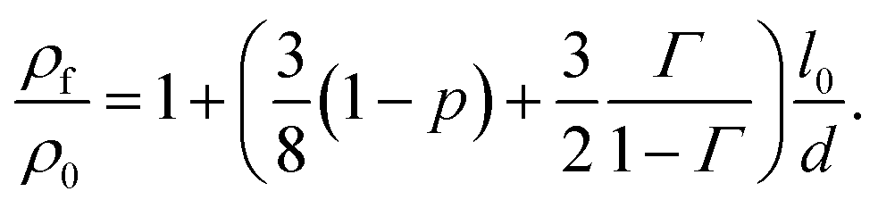
In this section, we introduce, a modelling approach to quantify the resistivity of a printed NP film as a result of film thickness and sintering time and temperature. Kasap et al. reported that electrons freely move in a grain of a film but get scattered at the grain boundaries.35 Hence, they concluded that surface and grain boundary electron scattering are the two dominant mechanisms that influence the resistivity in polycrystalline films. The Fuchs–Sondheimer (FS) and the Mayadas–Shatzkes (MS) model are commonly used to quantify the resistivity of a film as a result of its properties. The FS model accounts for the surface scattering while the influence of the grain boundary reflection is considered by the MS model.36–38 To obtain a more comprehensive theory, these models can be combined in a linear fashion, cf. e.g. ref. 39–42, resulting in
 | (1) |
Here, ρf and ρ0 are the resistivity of film and conventional bulk material, respectively; l0 is the electron mean free path; d is the thickness of the film; p is the surface scattering coefficient; and Γ is the reflection coefficient. Eqn (1) is applicable to films that do not require sintering to make them conducting; e.g., films that are prepared by various forms of physical vapor deposition. In this work, we extend the FS-MS model to make it suitable for printed and sintered NP films for various sintering conditions and film thicknesses.
When the morphology of the thin film is very grainy, the electrons are scattered at the grain boundaries. In this case, the mean electron free path l0 corresponds to good approximation to the average grain size G;35 it is l0 ≈ G. This correlation can be used to replace the electron mean free path which is very advantageous since the grain size depends on the sintering time t and temperature T. In detail, Kang30 noted that densification occurs by grain boundary diffusion and grain growth by surface diffusion so that the grain growth rate can be expressed as
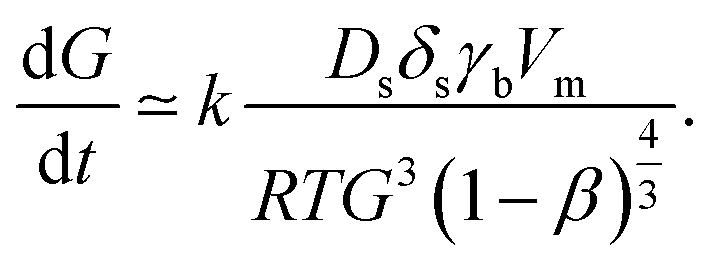 | (2) |
Here, Ds is the surface diffusion coefficient, δs is the grain boundary thickness, γb is the surface energy, R is the universal gas constant, Vm is the atomic volume, T is the temperature, t is the time and β is the relative density. Note that the original correlation in ref. 30 describes a proportionality between grain growth rate and the parameters above. We assume that by introduction of the proportionality constant k, the correlation can be quantified while this parameter mainly captures the NPs structure resulting from print process. At the beginning of the sintering process, the film consists of “grains” equal to the size of the particle d0. Therefore, we arrive in the initial condition G(t = 0) = d0 and integration of eqn (2) gives
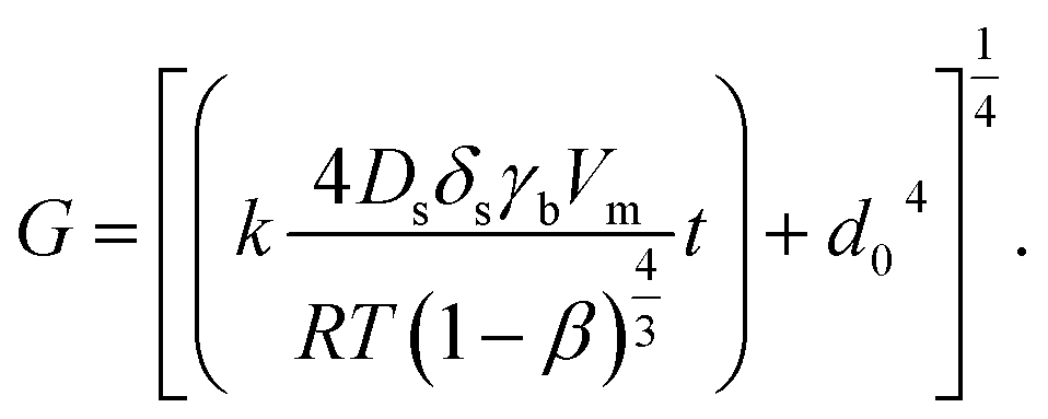 | (3) |
This expression can replace l0 in eqn (1) and we arrive after some rearrangements in
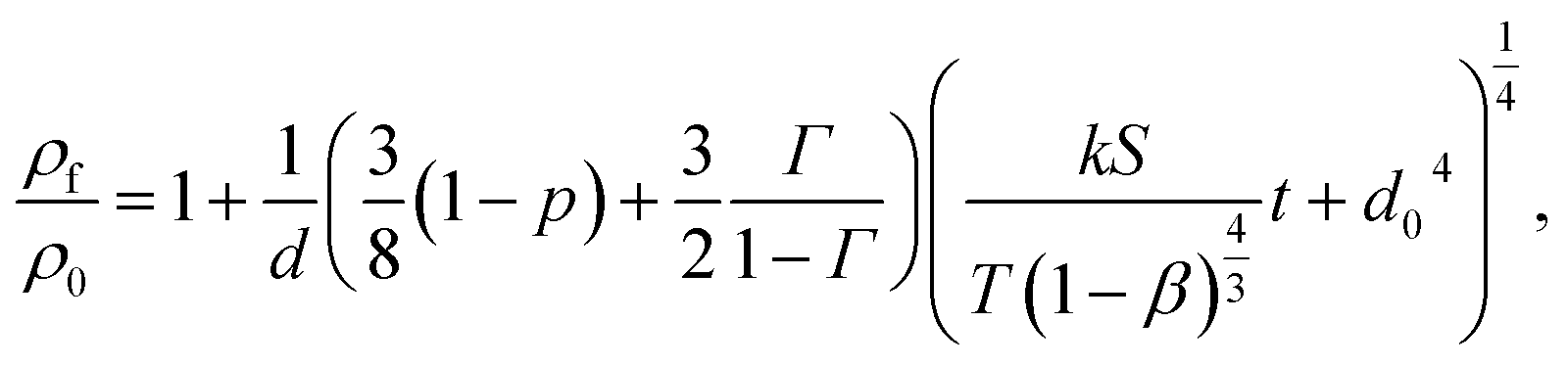 | (4) |
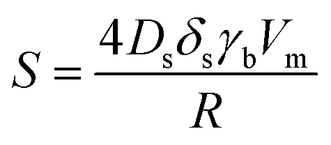 has the units m (s K)−1 and can be interpreted as a sintering coefficient. To summarize, the conventional FS-MS model is used to determine the resistivity of “homogeneously”-manufactured films, using physical or chemical vapor deposition, or thin sheets. In contrast, this modified model incorporates the grain growth depending on temperature and time and can therefore be applied for (printed) particulate structures that have to be sintered to make them electrically conductive. There are other factors which can strongly influence the conductivity of the thin films such as the surface chemistry in combination with residuals of solvent and the binder material. We inherently assume that there is no or only a minor influence of these factors which is proved by Energy-dispersive X-ray spectroscopy (EDS) measurements shown below.
4 Results and discussion
In this section, we first infer the parameter ranges that are required for the DOE. This is the most important step during the planning stage and often requires performing preliminary experiments. Then, the DOE is conducted and the influence of the parameters is discussed. Finally, the quality of the modified model is investigated.4.1 Determination of the DOE parameter range
At first, preliminary experiments are performed to infer a well-working multi-layer printing-sintering scheme as well as useful limits of the DOE parameter sintering temperature and time.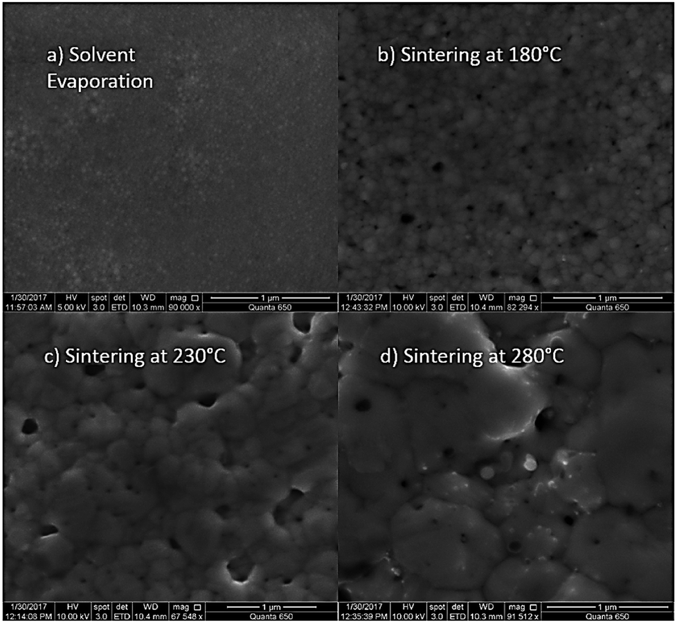 | ||
| Fig. 3 SEM image of the AgNP films after treatment with 1 μm scale at (a) 100 °C, (b) 180 °C, (c) 230 °C and (d) 280 °C for 30 minutes. | ||
In contrast, the larger grains and the necks formed between neighboring NPs in Fig. 3b indicate that the NP film after curing at the relatively-low temperature of 180 °C is to a certain degree sintered. The grain size distribution is relatively heterogeneous ranging from the original NP size to clusters of around 90 ± 15 nm. Additionally, some pores (void areas) are visible. Fig. 3c depicts the film morphology at the intermediate temperature of 230 °C. The SEM shows several large grains up to around 200 ± 50 nm size that consist of particles with interconnected grain boundaries to the neighboring particles. Though, there is still a considerable difference in size with the smallest particle clusters being around 100 ± 20 nm. Generally, it appears that fewer pores are present compared to the morphology at the lower temperature. Fig. 3d shows the film surface sintered at the highest temperature of 280 °C. Essentially, a densified structure with grain sizes ranging from around 250 to 530 nm is observed. Extensive neck growth diminished the single particle structure and very few but relatively large pores are observed.
In conclusion, we find that NPs sintering already takes place at temperatures well below the solvent boiling point. The sintering temperature has a profound influence on the grain size. The (average) neck radius of the particles at the highest temperature is around 15 times larger than that of the lowest temperature. Consequently, we use the solvent boiling temperature as the center temperature of the DOE. The DOE minimum temperature and time required to initiate the sintering is selected to be 180 °C and 30 min, respectively; the maximum temperature according to the DOE is then 280 °C. To investigate the effect of sintering time, we choose a maximum of 90 min which gives a DOE center time of 60 min. It should be noted that the DOE with the CCD design used in this study can provide significant information beyond the minimum and maximum temperature and time.
To obtain insight into the influence of the different schemes, we measure the resistivity and the thickness of the so-fabricated films; the results are compiled in Fig. 4a. The thickness of all three printed films is relatively similar and in the range of 4 to 5 microns. The influence of the printing–sintering scheme is more pronounced when it comes to the film resistivity. The measured resistivity of the P1, P2, and P3 scheme are 22.2, 29.9 and 25.2 × 10⁻⁹ Ωm, respectively. That is, a printed AgNP multi-layer film has the lowest resistivity when each layer is sintered before another layer is printed on top of it. Of course, this printing scheme results also in a cumulative sintering for the already sintered layers located beneath the top layer. However, this should have a minor influence on the resistivity as we conclude in Section 4.3.2.
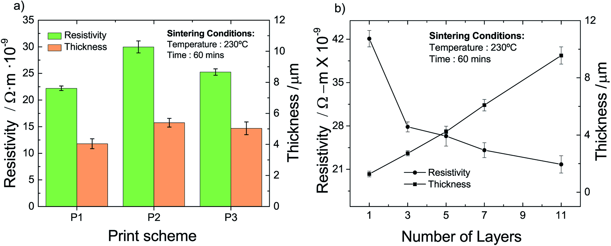 | ||
| Fig. 4 Thickness and resistivity of printed and sintered multi-layer films vs. (a) printing–sintering scheme and (b) number of layers for printing scheme P1. | ||
To obtain an indication of the layer range for the DOE, we prepare and analyze films fabricated with the P1 scheme and having a different number of layers; results are given in Fig. 4b. We identify a more or less linear increase of the film thickness with an increase of the number of layers. Two different behaviors can be recognized with respect to the resistivity. We find a pronounced resistivity drop from 42 to 28 × 10−9 Ωm for the relatively small increase of a single to a triple layer. When the number of layers is increased further, the resistivity decreases but to a relatively lesser extent. For example, the resistivity of a film with 7 layers is with around 24 × 10−9 Ωm only somewhat lower than that of the triple layer. Nevertheless, we observe that the resistivity continuously decreases with the number of layers. When we extrapolate the experimental data in Fig. 4b, we infer that a film approaches the regular silver (bulk) resistivity of 15.9 × 10⁻⁹ Ωm, if it consists of around 22 layers with an approximate thickness of 28 μm. Based on the results above, we choose the minimum, center and maximum number of layers to be three, six and nine, respectively.
4.2 Results of the DOE
We perform the experiments according to the DOE to systematically investigate the effect of the fabrication process on the properties of multi-layer AgNP films. All experimental results in the form of dependent variables (resistivity and thickness) depending on the process parameters (temperature, time and number of layers) are given in the ESI† to this article. Note that we give all results in the form of an inverted resistivity (conductivity) since this transformation increases the quality of regression. The full model derived from the fitting to the experiments is further investigated using the analysis of variance (ANOVA) method. The insignificant parameters from the model equation can be eliminated when the calculated probability is greater than 0.05. In detail, the ANOVA method gives the correlation between (inverse) resistivity ρ, number of printed layers n, sintering temperature T and time t according to
 | (5) |
All linear terms of the process parameters are included in the correlation but not all quadratic and mixed terms. When we analyse the coefficients along with typical values for the parameter, we can infer that both temperature linear and quadratic terms are dominating the correlation. However, since they have opposing signs the total influence is lowered. The same statements can be made for the sintering time. The accuracy of the DOE-based correlation is demonstrated in Fig. 5a by a parity plot where experimental conductivities are plotted against predicted data. We find good to very good agreement with a root mean square error of only 0.004 × 10⁻⁹ Ωm.
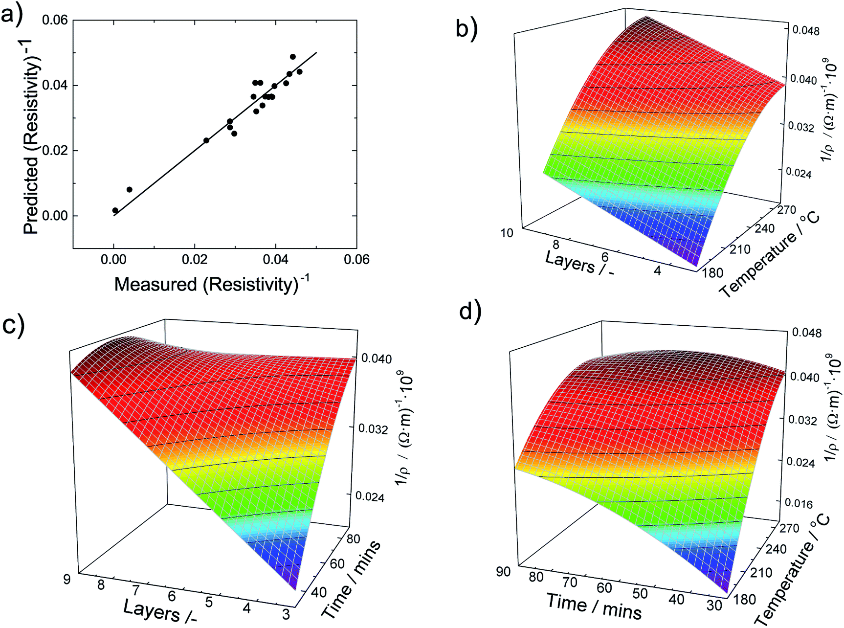 | ||
| Fig. 5 (a) Parity plot of predicted and measured inverse resistivity. Inverse resistivity vs. (b) sintering temperature and number of layers at a constant sintering time of 60 min; (c) sintering time and numbers of layers at a constant sintering temperature of 230 °C; (d) sintering temperature and time for a film made of 6 layers. | ||
To obtain further insight into the dependencies, eqn (5) is plotted in form of different three-dimensional surface plots in Fig. 5b–d by keeping one parameter at the central level while varying the other two within the experimental range. In detail, part (b) illustrates the influence of the number of layers and the sintering temperature for a sintering time of 60 minutes. The dependency is straightforward in terms that the highest conductivity is achieved at the highest temperature and number of layers. Part (c) gives the mutual influence of sintering time and number of layers at a sintering temperature of 230 °C. Generally, we find that the conductivity increases with sintering time and number of layers. However, the mutual influence is more complex here since the plot indicates a local conductivity minimum at the intermediate number of layers and time. Likewise, part (d) reflects the mutual influence of time and temperature for a film made of 6 layers and reveals a similar complex situation. Generally, we observe an increase of the conductivity when sintering time and temperature increase. But there is a (local) maximum conductivity which indicates that too high temperatures and times have a somewhat negative impact and result in a conductivity decline. To conclude, all these visualizations show that the interaction of the parameters are complex and the maximum conductivity is only achieved by an multivariable optimization of all process parameters based on the outcome of the DOE.
Similarly, we use the ANOVA method to evaluate the significance of the linear, mixed and quadratic terms that influence the thickness of the films and arrive in
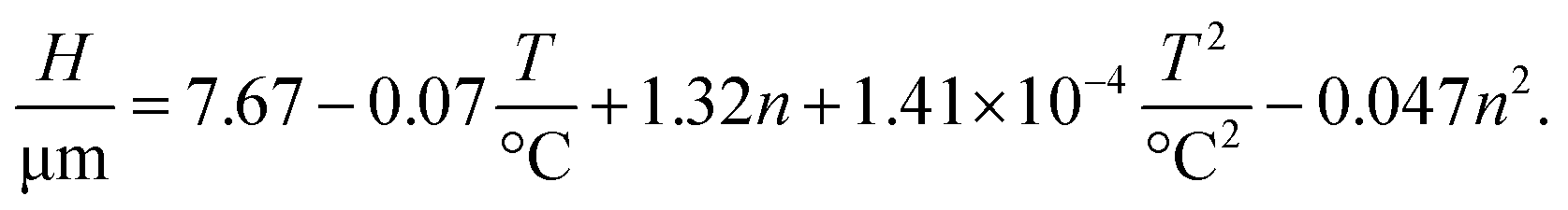 | (6) |
We note that there is no significant influence of the sintering time. Additionally, the correlation has no mixed terms and comprises only of the so-called main effects; i.e., terms with a single independent variable that influences the dependent variable. Since linear and quadratic terms of each parameter have opposing signs, an interpretation of the correlation is not right away available.
To test the quality of eqn (6), predicted and measured film thicknesses are shown as a parity plot in Fig. 6a. Generally, we find a very good agreement as indicated by the short distance of the data points to the diagonal of the plot. The root mean square error of the differences between predicted and observed values is 0.57 μm.
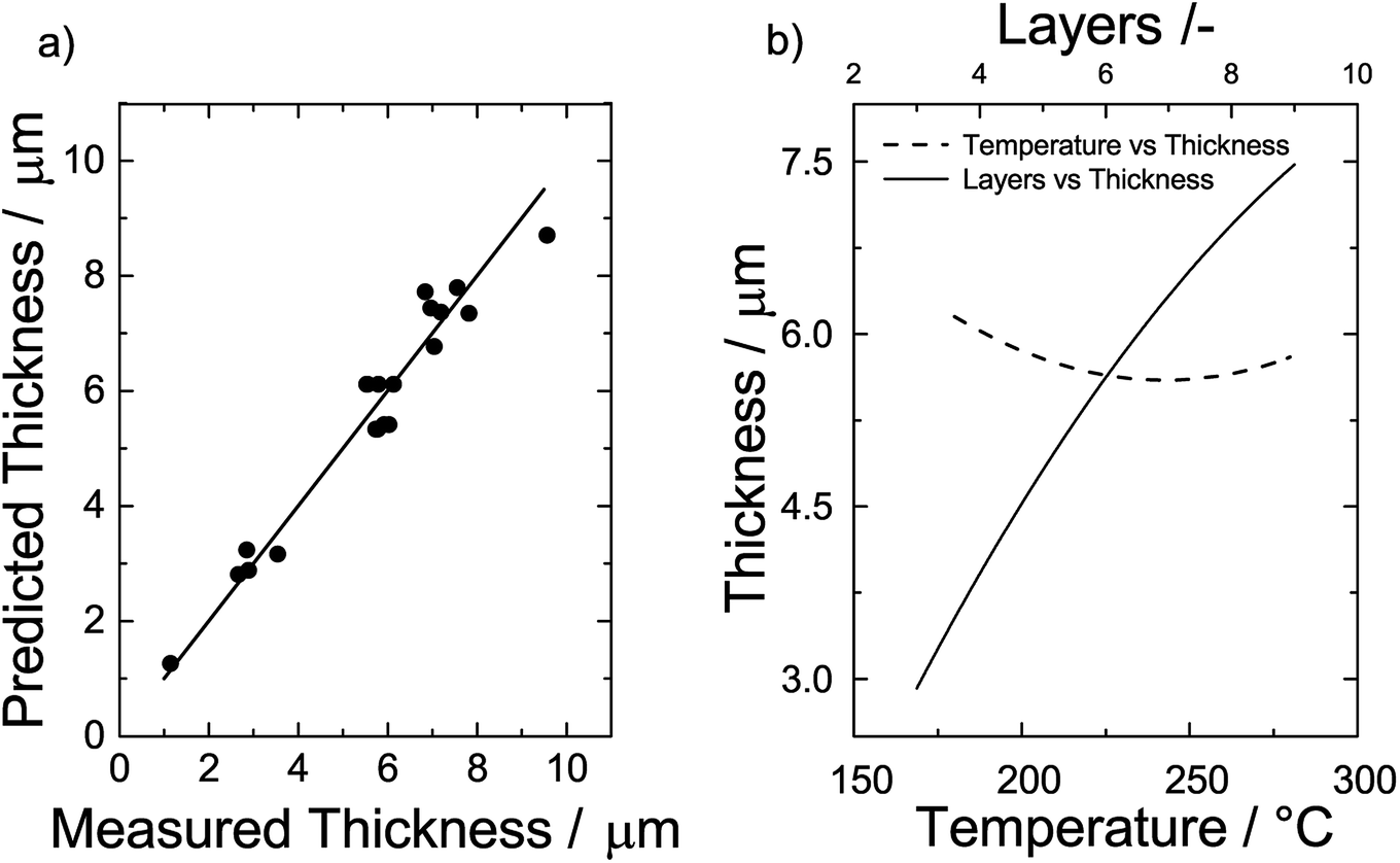 | ||
| Fig. 6 (a) Parity plot of the predicted thickness vs. the measured thickness and (b) effect of temperature (left y-axis) and number of layers on the film thickness (upper x-axis). | ||
To get detailed insights into the dependencies, we plot the film thickness for a film consisting of 6 layers vs. the sintering temperature on the left y-axis of Fig. 6b. We find that the film thickness initially decreases with an increase of the sintering temperature. At around 240 °C, there is a minimum and the thickness increases when the temperature is further increased. Likewise, we plot the film thickness vs. the number of printed layers sintered at a temperature of 230 °C on the upper x-axis of Fig. 6b. The effect of the number of layers is considerably higher than that of the temperature. To good approximation, the correlation is linear and a doubling of the number of layers results in a doubling of the film thickness.
To conclude, the DOE allows for a qualitative and quantitative interpretation of the influence of the process parameters on the properties of the multiple printed and sintered AgNP films. The resulting correlations can be used, for example, to optimize the conductivity of a printed film of desired thickness. For instance, if we would like to fabricate a AgNP film with a thickness of 5 μm and a minimum of electrical resistivity, we need to print 5 layers where each layer is sintered at 270 °C for 70 min. The resistivity of such a film corresponds then to 23.9 × 10⁻⁹ Ωm. Likewise, if we would like to have a film with a certain resistivity, we can choose the appropriate thickness and sintering temperature and time.
4.3 Analysis of the modified resistivity model
In this Section, we use literature and the experimental data of the DOE to validate the modified FS-MS model that we introduced in Section 3.| Parameter | Value | Ref. |
|---|---|---|
| Surface scattering coefficient p/— | 0.5 | — |
| Reflection coefficient Γ/— | 0.27 | Artuncç et al.44 |
| Relative density β/— | 0.8 | Bai et al.45 |
| Surface diffusivity Ds/(m2 s−1) | 3.13 × 10⁻²³ | Jiang et al.46 |
| Atomic volume Vm/(m3 mol−1) | 1.03 × 10⁻⁵ | Greer and Street29 |
| Surface energy γb/(J m−2) | 1.19 | Alymov et al.47 |
| Bulk resistivity ρo/(Ωm) | 15.9 × 10⁻⁹ | Greer and Street29 |
| Grain boundary thickness δs/m | 5 × 10⁻¹⁰ | Lee et al.48 |
In terms of the proportionality constant k, we make the assumption that we can use an average value that covers a certain range of films. Hence, we select two experiments with different conditions along with the literature data to calculate the respective k from eqn (4). In detail, we choose a 5-layers film sintered at 230 °C and 60 min and a 3-layers film sintered at 280 °C and 30 min and calculate the k values to be 2.27 × 10¹³ and 3.44 × 10¹³, respectively. Accordingly, we use an average regression parameter k of 2.85 × 10¹³ in the next subsection to verify the modified FS-MS model.
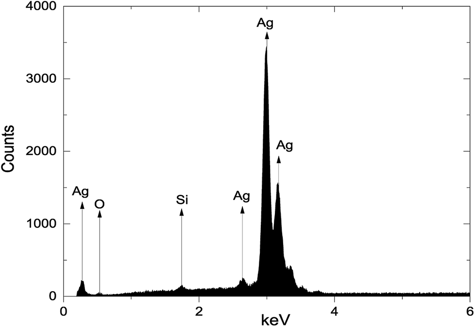 | ||
| Fig. 7 EDS of a single layer AgNP film after solvent evaporation at 100 °C for 30 minutes. | ||
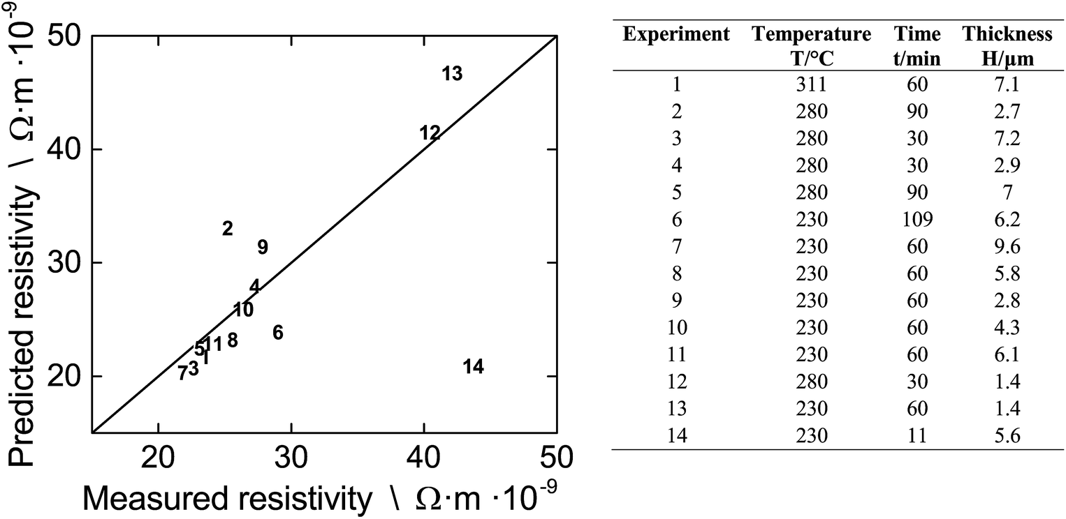
We test whether or not our modified FS-MS model along with the literature data and the average proportionality constant k can be employed to predict resistivities of differently fabricated multi-layer films. The left part of Fig. 8 gives the parity plot of predicted vs. measured resistivity for films that we prepared for the DOE. The right part is a detailed legend which gives the fabrication conditions.
 | ||
| Fig. 8 Verification of the resistivity model by comparison of predicted with experimental results. | ||
When we inspect Fig. 8, we find that the model does not only reflect the film resistivity of experiments 4 and 10, that we used to infer the average k from, but also predicts the majority of the other experiments with a very good accuracy. The prediction of experiments 2, 6, 9, and 13 is somewhat less accurate as indicated from the distance to the parity line while prediction of experiment 14 more or less fails. The limited accuracy of experiment 2, 9, and 13 can be attributed to the fact that they consist of single or dual layers. For this case, the spacing of the print droplets is very important and there are too few NPs per area resulting in a packing structure with holes and isolated NPs. This gives a non-uniform film during sintering as shown in Fig. 3 In contrast, printing more layers deposits more NPs per area, which improves the packing structure and lowers the defects. This results in a more uniform film during sintering with a different k value compared to the heterogenous film. The limited accuracy for experiment 6 is probably related to the extreme long sintering time which induces pore formation, thereby increasing the film resistivity which is not captured by the model. The failure of the model for experiment 14 is understood. Here, the short sintering time of 11 minutes is not sufficient for the formation of grains and we can assume that the film consists of layers of uncoalesced single NPs. Since the model is derived for films which consist of fused NPs due to sintering, we cannot expect to get accurate results for a case outside of its applicability. This is also the reason that the prediction of the resistivity of all DOE experiments at T = 180 °C (data not given in Fig. 8) and below fails. At these low temperatures, mainly solvent evaporation occurs and neck formation is not very advanced.
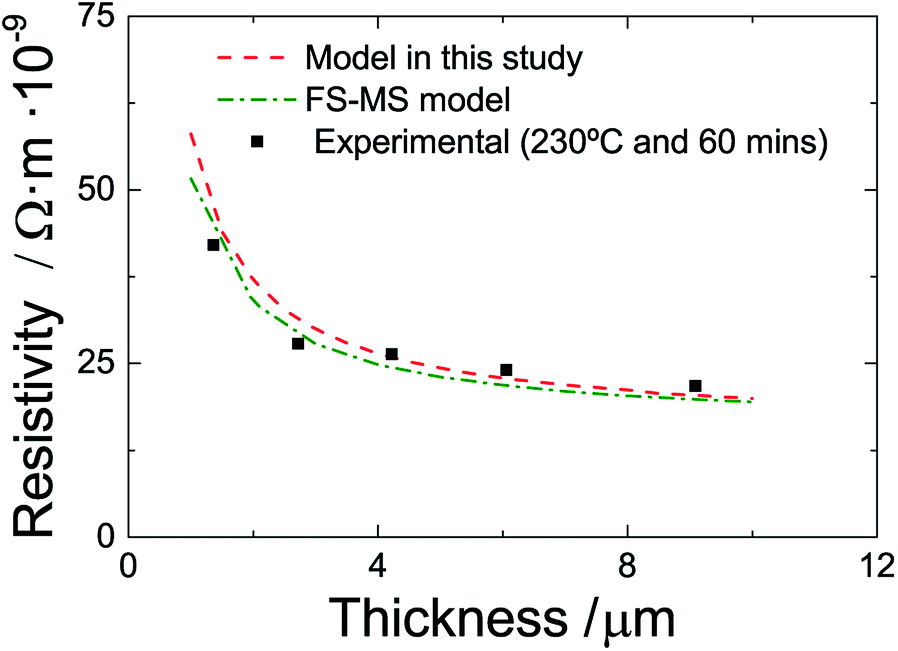
Finally, we compare the accuracy of our model with that of the conventional FS-MS model for experiments with constant sintering temperature and time but varying thickness (number of layers). Fig. 9 shows experimental and predicted data for films of various thickness that are sintered at 230 °C and 60 minutes. The FS-MS model is fitted to the experimental data as this is the standard way to infer the model parameter. Here, we use p = Γ = 0.5 and l0 = 3.2 × 10⁻⁶ m, which is the average grain size at these sintering conditions as predicted by our extended FS-MS model, as initial guess values. The resulting regression parameter are p = 0.77, Γ = 0.3 and l0 = 3.08 × 10⁻⁶ m. A comparison of the literature data that we engage in our modified model with these regression results shows a good agreement for the reflection coefficient and the electron mean free path. The surface scattering coefficient differs by approximately 50%. Here, the question arises whether this a mathematical artifact since for a multivariable regression different sets of regression coefficients may exist that all give good regression results. Or is this a true difference in material characteristics? The literature data that we employ is for a sputtered silver thin film and it is possible that there are differences in the grain morphology compared to a printed and sintered film. Though, we would then expect that there is also a distinct difference in the reflection coefficient which is not the case. If we assume that the surface scattering coefficient extracted from the FS-MS model is more realistic, we can perform another regression of our model and arrive in a new averaged k value of 3.08 × 10¹³ which is similar compared to the previous regression coefficient. This indicates that there is only a minor influence of the surface scattering coefficient to the film resistivity. This can also be inferred by fitting the single FS and the single MS model to the data. The FS model (surface scattering) can hardly be fitted to the data while the MS model (grain boundary reflection) shows an appropriate regression quality.
 | ||
| Fig. 9 Fitting the experimental data with FS-MS model and model in this study. | ||
Nonetheless, it is obvious in Fig. 8 that the conventional and the extended FS-MS model describe the resistivity of the sintered films for different film thicknesses very well. The major advantage is that our extended model incorporates the influence of sintering time and temperature. It utilizes mainly literature data but the coefficient k which we infer from only two experiments. And in contrast to the conventional FS-MS model, our approach predicts the resistivity of films sintered with different temperatures and times with a good accuracy while the FS-MS model requires fitting for each sintering temperature and time.
Note that there is an obvious discrepancy between the modelling approach and the experiments that we pursue. The model accounts only for the sintering time of the actual (top) layer that is sintered. However, our films consist of printed and sintered multi-layers so that sintering of the top layer continues the sintering of the layer beneath. The straightforward question is why the correlation still gives a good prediction of the influence of the time. On one hand, this is due to the fact that the influence of time in eqn (4) is in the form of a fourth root. Hence, the sintering time has a profound influence on the initial grain growth of the top layer but this cumulative time for the layers beneath has in comparison much less influence on their grain size.
5 Concluding remarks
This study is concerned with the fabrication of AgNP films by inkjet printing on glass substrates. We employ a Design Of Experiments (DOE) to infer the influence of the sintering time and temperature as well the number of printed layers on the resistivity of the films. Preliminary experiments are conducted to guide in the selection of a reasonable parameter range for the DOE. We find that the sintering of the NPs already takes place at temperatures well below the solvent boiling point. Still, both sintering temperature and time determine the grain size and distribution. We also infer the influence of the printing and sintering scheme and the preliminary study shows that for multi-layer films, the lowest resistivity is achieved when a printed layer is sintered before another layer is printed on top of it. The outcome of the preliminary study is utilized in the DOE and the corresponding experiments are conducted. The results of the experiments are analyzed with the analysis of variance method. The inferred correlations clarify the influence of each process parameter and can be used to fabricate films with desired features such as maximum electrical conductivity which is important for many applications such as current collectors or electrical sensors.Finally, we introduce a novel approach to correlate the printed film resistivity with the film thickness and sintering time and temperature by a modification of the well-known FS-MS model. Here, we assume that the electron average free mean path corresponds to the average grain size in the sintered film. This allows for the introduction of a correlation for the grain growth depending on the sintering time and temperature in the FS-MS model. We validate this modified FS-MS model against the experimental results of the DOE. All model parameters are selected from literature but a constant that arises from the model derivation which mainly captures geometrical properties resulting from the printing process. We use two different experiments to infer an average constant and this approach allows for accurate prediction of all films with more than two layers. Films with single or dual layers require a different fitting constant due to a high non-uniformity in the particle arrangement. The accuracy gets limited at the extremes of the sintering process. That is, when no or little sintering occurs and the film can be considered as a layer of isolated or little connected NPs as well as at higher temperatures and times when pore formation is promoted.
In future work, it would be interesting to investigate the influence of the NP surface energy on the sintering process. For examples, many NP inks can only be dispersed by means of adding stabilizing agents (surfactants, co-solvents etc.) which has considerable influence on particle and substrate surface properties. Additionally, we have not yet investigated the mechanical properties of the films. It would be of interest to learn about the conditions that are required to achieve good adherence to the substrate.
Conflicts of interest
There are no conflicts to declare.Acknowledgements
This research was funded by the Natural Sciences and Engineering Research Council of Canada and by an Ontario Early Researcher Award for D. P. J. B.References
- H. Sirringhaus, T. Kawase, R. Friend, T. Shimoda, M. Inbasekaran, W. Wu and E. Woo, Science, 2000, 290, 2123–2126 CrossRef PubMed.
- R. K. Venkata, A. Venkata, P. S. Karthik and S. P. Singh, RSC Adv., 2015, 5, 77760–77790 RSC.
- S.-Y. Kim, K. Kim, Y. Hwang, J. Park, J. Jang, Y. Nam, Y. Kang, M. Kim, H. Park and Z. Lee, et al., Nanoscale, 2016, 8, 17113–17121 RSC.
- M. Hilder, B. Winther-Jensen and N. Clark, J. Power Sources, 2009, 194, 1135–1141 CrossRef.
- G. Cai, P. Darmawan, M. Cui, J. Chen, X. Wang, A. L.-S. Eh, S. Magdassi and P. S. Lee, Nanoscale, 2016, 8, 348–357 RSC.
- L. Lan, J. Zou, C. Jiang, B. Liu, L. Wang and J. Peng, Frontiers of Optoelectronics, 2017, 1–24 CrossRef.
- V. Dua, S. P. Surwade, S. Ammu, S. R. Agnihotra, S. Jain, K. E. Roberts, S. Park, R. S. Ruoff and S. K. Manohar, Angew. Chem., Int. Ed., 2010, 49, 2154–2157 CrossRef PubMed.
- S. Wünscher, B. Seise, D. Pretzel, S. Pollok, J. Perelaer, K. Weber, J. Popp and U. S. Schubert, Lab Chip, 2014, 14, 392–401 RSC.
- B. W. An, J. H. Shin, S.-Y. Kim, J. Kim, S. Ji, J. Park, Y. Lee, J. Jang, Y.-G. Park and E. Cho, et al., Polymers, 2017, 9, 303 CrossRef.
- Z. Yin, Y. Huang, N. Bu, X. Wang and Y. Xiong, Chin. Sci. Bull., 2010, 55, 3383–3407 CrossRef.
- M. Singh, H. M. Haverinen, P. Dhagat and G. E. Jabbour, Adv. Mater., 2010, 22, 673–685 CrossRef PubMed.
- C. Yang, C. P. Wong and M. M. Yuen, J. Mater. Chem. C, 2013, 1, 4052–4069 RSC.
- H. W. Choi, T. Zhou, M. Singh and G. E. Jabbour, Nanoscale, 2015, 7, 3338–3355 RSC.
- S. H. Ko, H. Pan, C. P. Grigoropoulos, C. K. Luscombe, J. M. Fréchet and D. Poulikakos, Nanotechnology, 2007, 18, 345202 CrossRef.
- Y. Aleeva and B. Pignataro, J. Mater. Chem. C, 2014, 2, 6436–6453 RSC.
- Y. Li, Y. Wu and B. S. Ong, J. Am. Chem. Soc., 2005, 127, 3266–3267 CrossRef PubMed.
- H. Shirai, M. T. Nguyen, Y. Ishida and T. Yonezawa, J. Mater. Chem. C, 2016, 4, 2228–2234 RSC.
- B. W. An, J. H. Shin, S.-Y. Kim, J. Kim, S. Ji, J. Park, Y. Lee, J. Jang, Y.-G. Park and E. Cho, et al., Polymers, 2017, 9, 303 CrossRef.
- H. S. Lim, S. J. Kim, H. W. Jang and J. A. Lim, J. Mater. Chem. C, 2017, 5, 7142–7160 RSC.
- D.-Y. Shin, J. W. Han and S. Chun, Nanoscale, 2014, 6, 630–637 RSC.
- S.-P. Chen, Z.-K. Kao, J.-L. Lin and Y.-C. Liao, ACS Appl. Mater. Interfaces, 2012, 4, 7064–7068 Search PubMed.
- T. H. Van Osch, J. Perelaer, A. W. de Laat and U. S. Schubert, Adv. Mater., 2008, 20, 343–345 CrossRef.
- T. Öhlund, A. Schuppert, B. Andres, H. Andersson, S. Forsberg, W. Schmidt, H.-E. Nilsson, M. Andersson, R. Zhang and H. Olin, RSC Adv., 2015, 5, 64841–64849 RSC.
- J. Olkkonen, J. Leppäniemi, T. Mattila and K. Eiroma, J. Mater. Chem. C, 2014, 2, 3577–3582 RSC.
- J. Vaithilingam, M. Simonelli, E. Saleh, N. Senin, R. D. Wildman, R. J. Hague, R. K. Leach and C. J. Tuck, ACS Appl. Mater. Interfaces, 2017, 9, 6560–6570 Search PubMed.
- R.-Z. Li, A. Hu, D. Bridges, T. Zhang, K. D. Oakes, R. Peng, U. Tumuluri, Z. Wu and Z. Feng, Nanoscale, 2015, 7, 7368–7377 RSC.
- S. Magdassi, M. Grouchko, O. Berezin and A. Kamyshny, ACS Nano, 2010, 4, 1943–1948 CrossRef PubMed.
- M. Ashby, Acta Metall., 1974, 22, 275–289 CrossRef.
- J. R. Greer and R. A. Street, Acta Mater., 2007, 55, 6345–6349 CrossRef.
- S.-J. L. Kang, Sintering: densification, grain growth and microstructure, Butterworth-Heinemann, 2004 Search PubMed.
- G. Tomandl and P. Varkoly, Mater. Chem. Phys., 2001, 67, 12–16 CrossRef.
- I. E. Stewart, M. J. Kim and B. J. Wiley, ACS Appl. Mater. Interfaces, 2017, 9, 1870–1876 Search PubMed.
- D. C. Montgomery, G. C. Runger and N. F. Hubele, Engineering statistics, John Wiley & Sons, 2009 Search PubMed.
- L. J. Van der Pauw, Philips Res. Rep., 1958, 13, 1–9 Search PubMed.
- S. Kasap, C. Koughia, H. Ruda and R. Johanson, in Springer Handbook of Electronic and Photonic Materials, Springer, 2006, pp. 19–45 Search PubMed.
- A. Matthiessen and C. Vogt, Ann. Phys., 1864, 198, 19–78 CrossRef.
- K. Fuchs, Math. Proc. Cambridge Philos. Soc., 1938, 34, 100–108 CrossRef.
- E. H. Sondheimer, Adv. Phys., 1952, 1, 1–42 CrossRef.
- J. M. Cowley and A. F. Moodie, Acta Crystallogr., 1957, 10, 609–619 CrossRef.
- A. Mayadas and M. Shatzkes, Phys. Rev. B, 1970, 1, 1382 CrossRef.
- F. Thieme and W. Kirstein, Thin Solid Films, 1975, 30, 371–375 CrossRef.
- J. Sambles, Thin Solid Films, 1983, 106, 321–331 CrossRef.
- K.-S. Moon, H. Dong, R. Maric, S. Pothukuchi, A. Hunt, Y. Li and C. Wong, J. Electron. Mater., 2005, 34, 168–175 CrossRef.
- N. Artunç, M. Bilge and G. Utlu, Surf. Coat. Technol., 2007, 201, 8377–8381 CrossRef.
- J. G. Bai, Z. Z. Zhang, J. N. Calata and G.-Q. Lu, IEEE Trans. Compon. Packag. Technol., 2006, 29, 589–593 CrossRef.
- Q. Jiang, S. Zhang and J. Li, Solid State Commun., 2004, 130, 581–584 CrossRef.
- M. Alymov, E. Maltina and Y. Stepanov, Nanostruct. Mater., 1994, 4, 737–742 CrossRef.
- W. Lee, R. Eadie, G. Weatherly and K. Aust, Acta Metall., 1978, 26, 1837–1843 CrossRef.
Footnote |
| † Electronic supplementary information (ESI) available. See DOI: 10.1039/c8ra03627f |
| This journal is © The Royal Society of Chemistry 2018 |