
 Open Access Article
 This Open Access Article is licensed under a
 Creative Commons Attribution 3.0 Unported Licence
Improved electrical transport properties of an n-ZnO nanowire/p-diamond heterojunction
Dandan Sanga,
Qingru Wanga,
Qinglin Wang *a,
Dong Zhanga,
Haiquan Hua,
Wenjun Wang*a,
Bingyuan Zhanga,
Quli Fanac and
Hongdong Lib
*a,
Dong Zhanga,
Haiquan Hua,
Wenjun Wang*a,
Bingyuan Zhanga,
Quli Fanac and
Hongdong Lib
aSchool of Physics Science and Information Technology, Shandong Key Laboratory of Optical Communication Science and Technology, Liaocheng University, Liaocheng 252059, China. E-mail: wangqinglin@lcu.edu.cn; phywwang@163.com
bState Key Laboratory of Superhard Materials, Jilin University, Changchun 130012, China
cKey Laboratory for Organic Electronics & Information Displays, Institute of Advanced Materials, Nanjing University of Posts & Telecommunications, Nanjing 210046, China
First published on 13th August 2018
Abstract
A heterojunction of n-ZnO nanowire (NW)/p-B-doped diamond (BDD) was fabricated. The rectifying behavior was observed with the turn on voltage of a low value (0.8 V). The forward current at 5 V is 12 times higher than that of a larger diameter n-ZnO nanorod (NR)/p-BDD heterojunction. The electrical transport behaviors for the comparison of n-ZnO NWs/p-BDD and n-ZnO NRs/p-BDD heterojunctions are investigated over various bias voltages. The carrier injection process mechanism for ZnO NWs/BDD is analyzed on the basis of the proposed equilibrium energy band diagrams. The ZnO NWs/BDD heterojunction displays improved I–V characteristics and relatively high performance for the electrical transport properties.
1. Introduction
Zinc oxide is a suitable semiconductor because of its promising application in photodetectors,1–3 light-emitting diodes (LED),4 and solar cells5 on account of its wide bandgap (3.37 eV) and high electron mobility at room temperature.6 Multiple patterns of ZnO nanostructures, for example (e.g.) nanowires,7 nanorods,8 nanobelt,9 nanosheets10 have been extensively researched because of their excellent photoelectric properties compared to the bulk. Among the nanostructures above, ZnO nanowires (NWs) are more attractive due to their better carrier confinement and high density surface trap states,11 which can enhance the electrical properties and ultraviolet (UV) photodiodes performance of the devices.12,13 However, in virtue of the deep acceptor impurity states, low solubility dopants and the self-compensation effect, the intrinsically n-type semiconductor ZnO is difficult to manufacture with a p–n homo-junction architecture for many electronic and optical devices.14 Thus far, additional p-type substrate materials, for instance, Si,15 Cu2O,16 GaN,17 graphene,18 NiO,7 B-doped diamond film (BDD)19–22 and organic materials,23 have been exploited as the candidate to replace p-type ZnO semiconductors for the fabrication of pn heterojunctions. Among them, the B-doped diamond film (bandgap 5.47 eV) is appropriate as a high-temperature p-type conductive material. Up to the present, the electrical transport behavior at higher temperature,21 the ultraviolet photoelectrical properties19,24 and the photocatalytic activities25,26 of n-ZnO NRs/p-diamond heterojunctions have been investigated, however, the n-ZnO NRs/p-BDD heterojunctions have low forward current with 20–80 μA at 5 V.20,25,27In this work, we fabricated n-ZnO NWs/p-BDD heterojunction and obtained better I–V performance with forward current of 600 μA. We have made a detail analysis of the current–voltage (I–V) performance of 1D n-ZnO NWs/p-diamond heterojunction. The heterojunction parameters (the turn on voltage, the ideality factor and reverse leakage current etc.) and the electrical transport properties have been explored and discussed thoroughly for 1D n-ZnO NWs/p-diamond. The electrical properties of the 1D n-ZnO NWs/p-diamond heterojunction are significantly enhanced compared to the fabricated n-ZnO nanorods (NRs)/p-diamond heterojunction.
2. Experimental
Prior to the BDD growth, the hydrogen termination (111) oriented single crystal silicon wafer (1 cm × 1 cm) was immersed into the ethanol and acetone for 5 minutes ultrasonic cleaning, respectively. Then the p-type BDD film with a thickness of ∼4 μm was synthesized on the silicon wafers by chemical vapor deposition (CVD) method. The as grown ZnO NWs and NRs on BDD film was performed by hydrothermal approach. Prior to the hydrothermal procedure, ZnO seed layer with a thickness of ∼30 nm was grown by magnetron sputtering. 15 mL zinc acetate dehydrate (Zn(CH3COOH)2·2H2O) and 15 mL hexamethylenetetramine (HMT·C6H12N4) aqueous solution with 0.05 M for NWs and 0.1 M for NRs concentration were compound together, then maintain 10 min under slight magnetic mixing. The particular of the BDD, ZnO NWs and NRs deposited parameters can be discovered in our former work.18,22The morphologies and structures aspects of the as-fabricated ZnO and diamond were detected by scanning electron microscope (JEOL JXA-8200), the transmission electron microscopy (TEM) images were taken using a JEM-2100 transmission electron microscope with an operating voltage of 200 kV. Raman microscopy (514.5 nm line of an Ar+ ion laser), and X-ray diffraction (Rigaku D/MAX-RA with Cu Kα radiation of l = 1.54056 Å). The absorption spectra were analyzed by UV-Vis absorption spectroscopy (UV-3150 spectrophotometer). The I–V curves of the heterojunctions were tested by a Keithley 2400 source.
3. Results and discussions
SEM image displays the CVD BDD film with uniform grains by average diameter of ∼2 μm (Fig. 1(a)). The typical vertical-view SEM image of ZnO NWs and ZnO NRs are presented in Fig. 1(b) and (c), respectively. It is found that the ZnO NWs and NRs are generally grown vertically-aligned on the diamond grain planes. The average diameters and lengths of ZnO NWs (NRs) are 80 nm (600 nm) and 500 nm (2 μm), respectively. It is obvious that the diameter of the ZnO NWs is thinner than the ZnO NRs structure. Observed from the TEM (Fig. 1(d)), the ZnO NWs have a large aspect ratio with a smooth surface. Inset shows a typical HRTEM image of ZnO NWs which reveals that the growth of ZnO NWs are along the [0001] direction and the d-spacing was obtained to be 2.60 Å corresponding to the (100) planes of hexagonal ZnO. The ZnO NWs and NRs crystalline structures deposited on BDD substrates were investigated by XRD (Fig. 2(a)) and Raman microscopy (Fig. 2(b)) measurements. As shown of XRD pattern in Fig. 2(a), in addition to the diamond (111) facet diffractive peaks presented at 43.9°, the other main peaks are indexed to the (100), (002), (101), (102), and (103) diffractions peaks from ZnO hexagonal structure. In the Raman pattern (Fig. 2(b)), the 1332 cm−1 peak originates from the diamond intrinsic zone-centre phonon band,28 and the 332 cm−1, 437 cm−1 and 582 cm−1 peaks are indexed for the E2H–E1H, E1H and A1(LO) mode of ZnO, respectively.29 The XRD and Raman spectrum indicate the fabricated ZnO NWs and NRs deposited on the BDD substrate are with single crystal and mostly along the [0001] orientation. | ||
| Fig. 1 (a) SEM image with plane vertical view of BDD substrate, (b) SEM image of ZnO NWs deposited on the BDD substrates, (c) SEM image of ZnO NRs deposited on the BDD substrates, (d) TEM image of ZnO NWs, inset shows a typical HRTEM image of ZnO NWs. | ||
 | ||
| Fig. 2 (a) XRD and (b) Raman pattern of ZnO NWs and ZnO NRs on BDD substrates, respectively. | ||
The schematic of n-ZnO NWs/p-BDD heterojunction devices are depicted in top inset of Fig. 3. Two silver (Ag) wires are connected on BDD wafer as the positive electrodes. The n-type ZnO pressed with ITO is negative electrodes. The I–V performances of Ag/BDD and Ag/ITO both exhibits linear relation (bottom inset of Fig. 3) indicating the ohmic contact. In addition, ZnO-ITO is of ohmic contact attributed to the nearly similar work function of the two structure.30 Tested by Hall-effect instrument, the carrier density, the resistivity, and the mobility of the BDD is 1.5 × 1018 cm−3, 0.11 Ω cm, and 39.4 cm2 V−1 s−1, respectively.
 | ||
| Fig. 3 The I–V plots of the n-ZnO NWs/p-BDD and n-ZnO NRs/p-BDD heterojunction, respectively. The top inset is the schematic of n-ZnO NWs/p-BDD heterojunction device; the bottom inset is linear relation ohmic contacts measurements for Ag/BDD and Ag/ZnO. | ||
The I–V plots of the n-ZnO NWs/p-BDD and n-ZnO NRs/p-BDD heterojunction were shown Fig. 3. It displays well rectification properties with a rectify ratio of 19.3 and 7.8 at 5 V for the two heterojunction, respectively. The forward turn on voltage is 1.7 V for n-ZnO NRs/p-BDD heterojunctions, and decreased to 0.8 V for ZnO NWs/BDD. The turn on voltage fall to a lower value for ZnO NWs/BDD confirming a good quality interface properties. The reason for this is mainly owing to the generation of more free charge electrons in ZnO NWs to the heterojunction compared to ZnO NRs.31 Moreover, the turn-on voltage for the n-ZnO NWs/p-BDD device in this work is 10 times lower than the reported n-ZnO NWs/p-NiO heterojunction32 and 6 times lower than the n-ZnO NWs/p-Zn2GeO4 heterojunction.33 Importantly, compared to the fabricated n-ZnO NRs/p-BDD heterojunction, the larger rectification ratio and the lower turn on voltage of n-ZnO NWs/p-BDD suggest that the latter has relatively high performance.
The reverse leakage current is 30.47 μA and 6.45 μA at reverse bias of −5 V for ZnO NWs/BDD and ZnO NRs/BDD, respectively. The larger leakage current for ZnO NWs/BDD was mostly attributed to tunneling effect induced by the more trap centers and higher defect concentration from the interface compared to ZnO NRs/BDD heterojunction.31 It is noted that the forward current of ZnO NWs/BDD heterojunction is significantly increased. At the forward voltage of +5 V, the current is 607.2 μA, which is more than 12 times higher than the ZnO NRs/BDD heterojunction (52.7 μA). In virtue of the existence of more surface trap states of deep level in the 1D ZnO NWs,11 the ZnO NWs/BDD heterojunction with larger forward current thus exhibits improved I–V characteristics and better electrical transport properties compared to ZnO NRs/BDD heterojunction.
To deep-understand the mechanism of reduction of the turn on voltage and enlargement of the forward current for-ZnO NWs/BDD heterojunction, we propose a schematic energy band diagram at thermal equilibrium (Fig. 4(a)). As the electron barrier ΔEc is two times larger than the hole barrier ΔEv, the injection current is mainly caused by the injected holes from the valence band.20,21 Compared to ZnO NRs, the ZnO NWs presented more defect-level including deep levels, which are generally originate from the surface states oxygen vacancies and zinc interstitials.34 When the forward current is increased, the ZnO NWs deep levels band and bandgaps move up, the more injected holes from diamond valence band can tunnel to the deep levels of the ZnO NWs, forming a larger tunneling current. However, there exists less tunneling effect for ZnO NRs/BDD heterojunction. In addition, the as grown ZnO NWs possess more surface defects compared to ZnO NRs (inset in Fig. 4(b)). The higher density of oxygen from ambient air related surface trap states will adhere to the surface of ZnO NWs and act as trap centers. Then ZnO NWs can make the more negatively O2 charged, and produce a built-in barrier on the surface ZnO NWs. After the forward voltage is applied, thermal emission electron hole pairs are produced. The absorbed oxygen trap centers will capture more holes, leading to the separation and diffusion of the electron–hole pairs. The built-in barrier would prevent the electron hole pair's recombination and prolong the life of thermal emission carriers, resulting in much more free electrons injected from ZnO NWs conduction band to the diamond conduction band. Moreover, UV-Vis absorption spectra (Fig. 4(c)) were examined to further analyze the band gaps of the ZnO NWs and ZnO NRs. The band gap for ZnO NWs and NRs can be determined by the following formula,35
| αhν = D(hν − Eg) |
 | ||
| Fig. 4 (a) The energy band structure of the ZnO NWs/BDD heterojunction. (b) The plots of dI/dV with the voltage of the ZnO NWs/BDD and ZnO NRs/BDD devices, respectively. (c) UV-Vis absorption spectrum of the ZnO NWs and ZnO NRs grown on BDD. | ||
Differential conductivity (dI/dV) is the derivative of the I–V plots to obtain conduction properties in the heterojunction for it is directly proportional to the states density. Fig. 4(b) shows the variation plots in dI/dV with the applied bias voltage for both of ZnO NWs/BDD and ZnO NRs/BDD heterojunctions. For the ZnO NRs/BDD heterojunction, the dI/dV plots are almost constant as a result of the less charge carrier concentrations. However, for ZnO NWs/BDD heterojunction the dI/dV plots increases with the applied bias voltage, indicating an increase free charge carriers. Therefore, more oxygen trap centers in ZnO NWs/BDD heterojunction capture more holes, leading to an increase of free carriers which make an important contribution to the higher injected current.
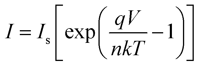
Semilog plots of I–V characteristics are in the inset of Fig. 5 for ZnO NWs/BDD and ZnO NRs/BDD heterojunctions. According to the thermionic emission model equation,
 | ||
Fig. 5 log![[thin space (1/6-em)]](https://www.rsc.org/images/entities/char_2009.gif) I–logV scale plots of the ZnO NWs/BDD and ZnO NRs/BDD heterojunctions, respectively (inset: the curve of the lnI–V). I–logV scale plots of the ZnO NWs/BDD and ZnO NRs/BDD heterojunctions, respectively (inset: the curve of the lnI–V). | ||
The logI–logV scale plots of the ZnO NWs/BDD and ZnO NRs/BDD heterojunctions are shown in Fig. 5. Both the two plots were separated into three different regions. At low voltage range (depicted region I, V < 0.75 V), the current transmission (I–V) follows a linear relation of ohmic law. For the moderately voltage of region II (0.75 V < V < 2 V), the forward current is following exponential regular increase and obeys a I–exp(αV) relationship, that is generally obtained from wide bandgap semiconductor heterojunction device results from the recombination tunneling principle.37 By fitting the curve of region II, the injection efficiency constant α is calculated to be 2.2 V−1 and 1.5 V−1 for the ZnO NWs/BDD and ZnO NRs/BDD heterojunction, respectively. Both values are close to 1.5 V−1, which indicates the fabricated ZnO NWs/BDD and ZnO NRs/BDD heterojunctions are ideal vacuum diodes.38 Moreover, a larger α indicates a higher thermal excited carrier injection.31 In this region, compared to ZnO NRs/BDD, the enlargement of α for ZnO NWs/BDD heterojunction can origin from the much more thermally emission carriers (electrons) induced by the more surface states, which fill the unoccupied traps.
When the forward bias voltage is higher than 2 V for region III (2 V < V < 5 V), the current transport properties according with the law of I–V3.4 and I–V2.6 for the ZnO NWs/BDD and ZnO NRs/BDD heterojunctions, respectively. The exponents value are higher than 2 normally ascribed to the space-charge-limited current (SCLC) transmission model.39,40 The high density trap states from the oxygen surface defect in the ZnO NWs/BDD heterojunction would capture thermal emission carriers (holes), leading to the jump of electrons into the diamond conduction band more easily. Therefore, in region III, the injected current obeys the trap-free SCLC mechanism with larger exponential than ZnO NRs/BDD heterojunction.
4. Conclusions
In summary, a heterojunction of n-ZnO NWs/p-BDD diode device have been fabricated. The larger tunneling current from diamond valence band to the deep levels of the ZnO NWs and more oxygen trap centers in ZnO NWs lowered the turn on voltage of the n-ZnO NWs/p-BDD heterojunction and promote the rectification ratio, whereas the forward current at 5 V is 12 times higher. It is proposed that the ZnO NWs/BDD heterojunction exhibits overall improved I–V characteristics and electrical transport properties with relatively high performance. The fabricated ZnO NWs/BDD heterojunction offers a promising design with a high performance for the developing of optoelectronic nanodevice, especially working at nano-scale and severe environments.Conflicts of interest
There are no conflicts to declare.Acknowledgements
This work was supported by the National Natural Science Foundation of China (Grant No. 11604133, 61405085, 61775089, 51472105 and 51502107), the National Key R&D Program of China (Grant No. 2016YFB0402105), the Shandong Provincial Natural Science Foundation (Grant No. ZR2017QA013), the Industrial Alliance Fund of Shandong Provincial Key Laboratory (Grant No. SDKL2016038), the Open Project of State Key Laboratory of Superhard Materials (Jilin University, Grant No. 201503 and 201612), the Project of Science and Technology Plan for University of Shandong Province (J16LJ05), the Initial Foundation for Doctor Program of Liaocheng University (Grant No. 318051612 and 318051610), and the Special Construction Project Fund for Shandong Province Taishan Scholars.References
- W. Wang, J. Qi, Q. Wang, Y. Huang, Q. Liao and Y. Zhang, Nanoscale, 2013, 5, 5981–5985 RSC.
- A. O. Dikovska, D. Pallotti, S. Lettieri, G. Atanasova, G. Avdeev, P. Maddalena, S. Amoruso and N. Nedyalkov, Appl. Surf. Sci., 2017, 423, 977–982 CrossRef.
- C. Tian, D. Jiang, B. Li, J. Lin, Y. Zhao, W. Yuan, J. Zhao, Q. Liang, S. Gao and J. Hou, ACS Appl. Mater. Interfaces, 2014, 6, 2162–2166 CrossRef PubMed.
- X. M. Zhang, M. Y. Lu, Y. Zhang, L. J. Chen and Z. L. Wang, Adv. Mater., 2009, 21, 2767–2770 CrossRef.
- J. Jean, S. Chang, P. R. Brown, J. J. Cheng, P. H. Rekemeyer, M. G. Bawendi, S. Gradečak and V. Bulović, Adv. Mater., 2013, 25, 2790–2796 CrossRef PubMed.
- M. H. Huang, S. Mao, H. Feick, H. Yan, Y. Wu, H. Kind, E. Weber, R. Russo and P. Yang, Science, 2001, 292, 1897 CrossRef PubMed.
- Y.-R. Li, C.-Y. Wan, C.-T. Chang, W.-L. Tsai, Y.-C. Huang, K.-Y. Wang, P.-Y. Yang and H.-C. Cheng, Vacuum, 2015, 118, 48–54 CrossRef.
- T. Dixit, I. A. Palani and V. Singh, RSC Adv., 2018, 8, 6820–6833 RSC.
- W. Q. Li, S. Y. Gao, L. Li, S. J. Jiao, H. T. Li, J. Z. Wang, Q. J. Yu, Y. Zhang, D. B. Wang and L. C. Zhao, Chem. Commun., 2016, 52, 8231–8234 RSC.
- S. J. Young and Y. H. Liu, RSC Adv., 2017, 7, 14219–14223 RSC.
- C. Soci, A. Zhang, B. Xiang, S. A. Dayeh, D. Aplin, J. Park, X. Bao, Y.-H. Lo and D. Wang, Nano Lett., 2007, 7, 1003–1009 CrossRef PubMed.
- Y. Li, F. Della Valle, M. Simonnet, I. Yamada and J.-J. Delaunay, Nanotechnology, 2008, 20, 045501 CrossRef PubMed.
- G. Chai, O. Lupan, L. Chow and H. Heinrich, Sens. Actuators, A, 2009, 150, 184–187 CrossRef.
- Y. I. Alivov, Ü. Özgür, S. Doğan, D. Johnstone, V. Avrutin, N. Onojima, C. Liu, J. Xie, Q. Fan and H. Morkoç, Appl. Phys. Lett., 2005, 86, 241108 CrossRef.
- L. Duan, P. Wang, F. Wei, X. Yu, J. Fan, H. Xia, P. Zhu and Y. Tian, J. Alloys Compd., 2014, 602, 290–293 CrossRef.
- I. H. Yoo, S. S. Kalanur, S. Y. Lee, G. R. Uhm, H. Jeon and H. Seo, RSC Adv., 2016, 6, 82900–82906 RSC.
- R. Li, C. Yu, H. Dong, W. Jia, T. Li, Z. Zhang and B. Xu, RSC Adv., 2017, 7, 49613–49617 RSC.
- Y.-T. Kwon, S.-O. Kang, J.-A. Cheon, Y. Song, J.-J. Lee and Y.-H. Choa, Appl. Surf. Sci., 2017, 415, 2–7 CrossRef.
- D. Sang, H. Li, S. Cheng, Q. Wang, J. Liu, Q. Wang, S. Wang, C. Han, K. Chen and Y. Pan, RSC Adv., 2015, 5, 49211–49215 RSC.
- H. Li, D. Sang, S. Cheng, J. Lu, X. Zhai, L. Chen and X.-q. Pei, Appl. Surf. Sci., 2013, 280, 201–206 CrossRef.
- D. Sang, H. Li, S. Cheng, Q. Wang, Q. Yu and Y. Yang, J. Appl. Phys., 2012, 112, 036101 CrossRef.
- M. Davydova, A. Laposa, J. Smarhak, A. Kromka, N. Neykova, J. Nahlik, J. Kroutil, J. Drahokoupil and J. Voves, Beilstein J. Nanotechnol., 2018, 9, 22 CrossRef PubMed.
- O. Game, U. Singh, T. Kumari, A. Banpurkar and S. Ogale, Nanoscale, 2014, 6, 503–513 RSC.
- Y. Wan, S. Gao, L. Li, J. Zhang, H. Fan, S. Jiao, J. Wang, Q. Yu and D. Wang, J. Mater. Sci.: Mater. Electron., 2017, 28, 11172–11177 CrossRef.
- Q. Yu, J. Li, H. Li, Q. Wang, S. Cheng and L. Li, Chem. Phys. Lett., 2012, 539, 74–78 CrossRef.
- Y. Li, H. Li, M. Li, C. Li, Y. Lei, D. Sun and B. Yang, J. Alloys Compd., 2018, 743, 187–195 CrossRef.
- C. D. Wang, S. K. Jha, Z. H. Chen, T. W. Ng, Y. K. Liu, M. F. Yuen, Z. Z. Lu, S. Y. Kwok, J. A. Zapien, I. Bello, C. S. Lee and W. J. Zhang, J. Nanosci. Nanotechnol., 2012, 12, 4560–4563 CrossRef PubMed.
- A. C. Ferrari and J. Robertson, Phys. Rev. B, 2000, 61, 14095 CrossRef.
- M. Rajalakshmi, A. K. Arora, B. Bendre and S. Mahamuni, J. Appl. Phys., 2000, 87, 2445–2448 CrossRef.
- Y. Yang, Q. Liao, J. Qi, Y. Zhang, L. Tang and N. Ye, Appl. Phys. Lett., 2008, 93, 133101 CrossRef.
- S.-Y. Liu, T. Chen, Y.-L. Jiang, G.-P. Ru and X.-P. Qu, J. Appl. Phys., 2009, 105, 114504 CrossRef.
- B. O. Jung, Y. H. Kwon, D. J. Seo, D. S. Lee and H. K. Cho, J. Cryst. Growth, 2013, 370, 314–318 CrossRef.
- B. Cao, J. Chen, R. Huang, Y. H. Ikuhara, T. Hirayama and W. Zhou, J. Cryst. Growth, 2011, 316, 46–50 CrossRef.
- A. B. Djurišić and Y. H. Leung, Small, 2010, 2, 944–961 CrossRef PubMed.
- S. T. Tan, B. J. Chen, X. W. Sun, W. J. Fan, H. S. Kwok, X. H. Zhang and S. J. Chua, J. Appl. Phys., 2005, 98, 1897 Search PubMed.
- N. Koteeswara Reddy, Q. Ahsanulhaq, J. Kim and Y. Hahn, Appl. Phys. Lett., 2008, 92, 043127 CrossRef.
- J. Ye, S. Gu, S. Zhu, W. Liu, S. Liu, R. Zhang, Y. Shi and Y. Zheng, Appl. Phys. Lett., 2006, 88, 182112 CrossRef.
- R. Forman, Phys. Rev., 1961, 123, 1537 CrossRef.
- Y. I. Alivov, J. Van Nostrand, D. C. Look, M. Chukichev and B. Ataev, Appl. Phys. Lett., 2003, 83, 2943–2945 CrossRef.
- I.-S. Jeong, J. H. Kim and S. Im, Appl. Phys. Lett., 2003, 83, 2946–2948 CrossRef.
| This journal is © The Royal Society of Chemistry 2018 |