
 Open Access Article
 This Open Access Article is licensed under a Creative Commons Attribution-Non Commercial 3.0 Unported Licence
Enhanced efficiency of Cu2ZnSn(S,Se)4 solar cells via anti-reflectance properties and surface passivation by atomic layer deposited aluminum oxide
Bingye Zhang *a,
Lu Hana,
Shitian Yinga,
Yongfeng Lib and
Bin Yao*b
*a,
Lu Hana,
Shitian Yinga,
Yongfeng Lib and
Bin Yao*b
aDepartment of Physics, Dalian University of Technology, Dalian, Liaoning 116023, P. R. China. E-mail: byzhang@dlut.edu.cn
bKey Laboratory of Physics and Technology for Advanced Batteries (Ministry of Education), College of Physics, Jilin University, Changchun 130012, China. E-mail: binyao@jlu.edu.cn
First published on 24th May 2018
Abstract
Reducing interface recombination losses is one of the major challenges in developing Cu2ZnSn(S,Se)4 (CZTSSe) solar cells. Here, we propose a CZTSSe solar cell with an atomic layer deposited Al2O3 thin film for surface passivation. The influence of passivation layer thickness on the power conversion efficiency (PCE), short-circuit current density (Jsc), open-circuit voltage (Voc) and fill factor (FF) of the solar cell is systematically investigated. It is found that the Al2O3 film presents notable antireflection (AR) properties over a broad range of wavelengths (350–1000 nm) for CZTSSe solar cells. With increasing Al2O3 thickness (1–10 nm), the average reflectance of the CZTSSe film decreases from 12.9% to 9.6%, compared with the average reflectance of 13.6% for the CZTSSe film without Al2O3. The Al2O3 passivation layer also contributes to suppressed surface recombination and enhanced carrier separation. Passivation performance is related to chemical and field effect passivation, which is due to released H atoms from the Al–OH bonds and the formation of Al vacancies and O interstitials within Al2O3 films. Therefore, the Jsc and Voc of the CZTSSe solar cell with 2 nm-Al2O3 were increased by 37.8% and 57.8%, respectively, in comparison with those of the unpassivated sample. An optimal CZTSSe solar cell was obtained with a Voc, Jsc and η of 0.361 V, 33.78 mA and 5.66%. Our results indicate that Al2O3 films show the dual functions of AR and surface passivation for photovoltaic applications.
1. Introduction
Recently, it has been proven that the conversion efficiencies of Cu(In,Ga)Se2 (CIGS) thin film solar cells can reach 22.6%, which is comparable to their Si counterparts.1,2 However, the shortage and high material cost of indium and gallium restrict the development of CIGS solar cells. Kesterite Cu2ZnSn(S,Se)4 (CZTSSe) has attracted much more attention as a promising substitute for CIGS solar cells on account of its outstanding optoelectronic properties and earth abundant, as well as non-toxic, constituents.3,4 The kesterite structure of CZTSSe is derived from the chalcopyrite crystal structure of CIGS, where Zn2+ and Sn4+ ions replace an equal number of In3+ and Ga3+ ions.5,6 Since it has similar properties to CIGS solar cells, the structure of a CZTSSe solar cell is adopted directly from CIGS photovoltaic technology, including a Mo bottom electrode, a chemical bath deposited CdS buffer layer, a transparent conducting oxide (TCO) stack of indium tin oxide (ITO)/ZnO etc. Recently, the conversion efficiency record of CZTSSe solar cells has been proven to be 12.6% using a hydrazine solution based method.7 However, the efficiency of CZTSSe solar cells remains far from that of CIGS solar cells. To decrease the efficiency gap between CZTSSe and CIGS solar cells, one of the major challenges is reducing surface carrier recombination, which is caused by grain boundaries, defects and states. Various technologies have been utilized to fabricate high quality CZTSSe films, such as thermal coevaporation, sputtering, pulsed-laser deposition and other non-vacuum-deposition technologies (e.g. electrodeposition and solution processing).8–11 However, due to the complexity of multernary materials, it is difficult to obtain high quality CZTSSe films with a low density of defects and states at the interface between CZTSSe and CdS. Thus, CZTSSe devices suffer from an open-circuit voltage (Voc) deficit caused by the significant recombination of photo-excited carriers due to the existence of large amounts of defects/states at the interface between CZTSSe and CdS.12,13 To solve this problem, it is necessary to induce a passivation layer to depress recombination. On one hand, a proper passivation layer can not only saturate dangling bonds to decrease the density of surface states in CZTSSe films (called chemical passivation), but also reduce the surface recombination velocity (Seff) due to the existence of fixed charge in the passivation layer (called field effect passivation).14,15 On the other hand, passivation layers can also prevent atomic interdiffusion between different layers in PV devices.16,17 Several dielectric materials have been used as passivation layers in CZTS-based solar cells and other PV devices (CIGS, Si solar cells etc.), such as Al2O3, TiO2, Si3N4 and ZrO2.18–22 Among these materials, Al2O3 has been regarded as a favorable material owing to its high dielectric constant, high transmission and large bandgap (6.3 eV), and is able to passivate p- and n-type semiconductors effectively.23,24 Recently, atomic layer deposition (ALD) has been proven to be an optimal technique for the synthesis of virtually pinhole-free inorganic thin films due to its low temperature deposition and precise thickness control. Moreover, atomic layer deposited Al2O3 (ALD-Al2O3) can provide a state-of-the-art level of surface passivation on c-Si (Seff < 2 cm s−1) and CIGS solar cells (Seff < 14 cm s−1).25,26 These low Seff values for Al2O3 passivated Si and CIGS solar cells are attributed to the high density negative fixed charge (Qf = 1012–1013 cm−2) in Al2O3 and the low interface-trap charge density (Dit = 1010–1012 eV−1 cm−2) at the interfaces of Al2O3/Si and Al2O3/CIGS. These positive results for the Al2O3 passivation layer and the beneficial technical aspects of ALD itself suggest that they would be appropriate for the passivation of CZTSSe solar cells.As is well known, the thickness of Al2O3 plays an important role in the density of interface states and the negative fixed charge for Si solar cells.27 Therefore, identifying the optimal thickness of Al2O3 thin film has become the critical factor for obtaining high passivation performance for CZTSSe solar cells. However, few reports describe the influence of Al2O3 thickness on the device performance of CZTSSe solar cells. Moreover, due to the differences in the structural, electronic and defect properties of CZTSSe and Si, as well as CIGS, the dominant passivation mechanism of Al2O3 on CZTSSe is still unclear.
In this study, CZTSSe films (Cu/(Zn + Sn) = 0.81 and S/(S + Se) = 0.12) coated with various thicknesses of ALD-Al2O3 (1–10 nm) film were fabricated. The influence of Al2O3 thickness on the optical and electrical properties of CZTSSe solar cells was investigated in detail. We demonstrate that ALD-Al2O3 thin films can not only provide a passivation effect, but also show excellent antireflection (AR) properties at short wavelengths for CZTSSe solar cells, which improves the power conversion efficiency (PCE), Voc, FF and short-circuit current density (Jsc) of the CZTSSe solar cells. A CZTSSe solar cell with a PCE of 5.66% has been achieved via adjusting the thickness of the Al2O3 thin film.
2. Experimental section
2.1. Materials and syntheses
 | (1) |
 | (2) |
The ALD-Al2O3 thin films were fabricated at 220 °C, and then annealed in situ at 400 °C for 10 min in N2 to activate surface passivation. Various thicknesses of the Al2O3 thin films were obtained via controlling the deposition cycles, and the growth rate of Al2O3 was 0.7 Å per cycle. Each cycle consisted of a TMA pulse (0.03 s), an N2 purge (12 s), a water pulse (0.06 s) and an N2 purge (12 s).
2.2. Characterization
The structure, surface morphology and compositional ratio of CZTSSe films were measured using scanning electron microscope (SEM) measurements on a Hitachi S-4800 equipped with an energy-dispersive X-ray spectroscopy (EDS) system (EDAX Genesis 2000). The crystal structures of the CZTSSe films were characterized using an X-ray diffractometer (XRD) with Cu Kα radiation (λ = 1.5406 Å). Optical reflectance of the CZTSSe films with ALD-Al2O3 thin films was detected using a spectrophotometer with an integrating sphere. X-ray photoelectron spectroscopy (XPS) analysis was used to identify the actual composition and chemical state of the grown Al2O3 thin films. For the PCE measurements of the CZTSSe solar cells, current density–voltage curves were measured using a Keithley 2400 source meter and a solar simulator (Abet Sun 2000; AM 1.5). The light intensity was calibrated to 100 mW cm−2 using a Newport optical power meter (model 842-PE) certified by Newport. The external quantum efficiency (EQE) curves were measured using a Zolix SCS100 QE system equipped with a 150 W xenon light source, a lock-in amplifier and an integrating sphere.3. Results and discussion
In general, most passivation materials need a post deposition annealing (PDA) process to activate the passivation effect.17 In some cases, the annealing treatment can cause the deterioration of crystalline quality for the films deposited under low temperatures, leading to more defects and impurities. Thus, SEM and XRD measurements were carried out to specify whether PDA could cause degradation. Fig. 1 shows top-view and cross-sectional SEM images for the CZTSSe films and the devices. Both of the CZTSSe films, with and without the Al2O3 thin film, exhibit a compact and dense morphology with a grain size ranging from 1–2 μm, as shown in Fig. 1(a) and (b). Fig. 1(c) and (d) show cross-sectional SEM images of the CZTSSe solar cell, which consists of a 1 μm Mo film, a 1.17 μm CZTSSe film, a 2 nm Al2O3 thin film, and a 50 nm CdS film, as well as a 300 nm i-ZnO/ITO film. It can be seen that the compactness and domain size of CZTSSe coated with Al2O3 thin film aren’t obviously changed compared with the unpassivated sample, which demonstrates that the deposition and annealing processes of Al2O3 have a faint effect on the surface morphology and the grain growth of CZTSSe films. It should be noted that some holes exist at the interface between CZTSSe and Mo, which is assigned to the unstable nature of CZTSSe in contact with Mo.28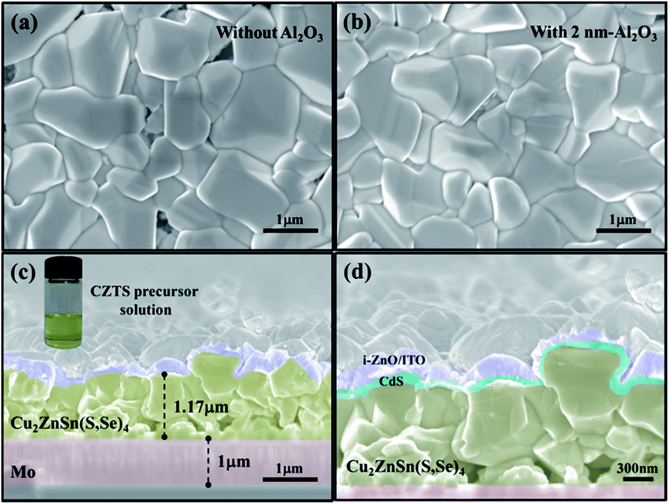 | ||
| Fig. 1 Top-views of the CZTSSe film with and without Al2O3 thin film (a and b), deposited on a Mo-coated SLG substrate. Cross-sectional SEM images of the CZTSSe solar cell with the structure SLG/Mo/CZTSSe/Al2O3 (2 nm)/CdS/i-ZnO/ITO/Al grid (c and d). | ||
Fig. 2 shows the XRD patterns of CZTSSe films, with and without Al2O3 thin film. The XRD patterns of the CZTSSe films show that all of the films can be indexed in kesterite-type structures with no secondary phases.29 With reference to JCPDS no. 00-026-0575 and 00-052-0868, three major diffraction peaks located at 27.34°, 45.45° and 53.81° are observed, which can be assigned to the (112), (220) and (312) planes, respectively, implying the good crystallinity of CZTSSe films. In addition, a minor peak located at 36.40° is also observed, corresponding to the (211) diffraction plane, as shown in Fig. 2(a). Fig. 2(b) shows the XRD pattern of the CZTSSe film with 2 nm Al2O3 thin film. Besides the diffraction peaks of CZTSSe, it can be clearly seen that no diffraction peak belonging to Al2O3 can be observed, suggesting the amorphous phase of the ALD-Al2O3 thin film. Moreover, the XRD peak position and full width at half-maximum (FWHM) of CZTSSe shows little change after the Al2O3 deposition and PDA processes. These results indicate that the processes of Al2O3 deposition and PDA have no obvious influence on the crystalline quality of CZTSSe film, which is consistent with the SEM results.
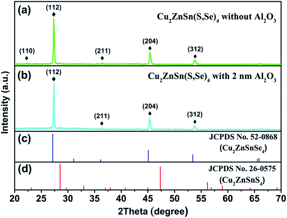 | ||
| Fig. 2 XRD patterns of CZTSSe films (a) without Al2O3 thin film and (b) with 2 nm Al2O3 thin film, as well as the standard patterns for (c) CZTSe (JCPDS no. 82-0868) and (d) CZTS (JCPDS no. 26-0575). | ||
For quantitative phase analysis, the full profile Rietveld refinement of the XRD pattern of the CZTSSe powder was carried out, as shown in Fig. 3. The structural model was refined on the basis of the tetragonal kesterite-type crystal structure [space group: I![[4 with combining macron]](https://www.rsc.org/images/entities/char_0034_0304.gif) (no. 82)]. The obtained structural parameters of CZTSSe are a = 5.6573 Å, c = 11.301 Å, and c/a = 2.00. The corresponding weighted residual error (Rwp), residual of least-squares refinement (Rp) and χ2 of the fittings are 5.87%, 4.46%, and 2.38, indicating good fits of the patterns. These lattice parameters (a and c) are slightly decreased compared to the reported values of CZTSe (ICSD#95117). This decreasing of the lattice parameters can be assigned to the shrinkage of the unit cell due to the substitution of Se atoms with S, which have a smaller ionic radius (1.84 Å) compared to that of Se (1.98 Å).30
(no. 82)]. The obtained structural parameters of CZTSSe are a = 5.6573 Å, c = 11.301 Å, and c/a = 2.00. The corresponding weighted residual error (Rwp), residual of least-squares refinement (Rp) and χ2 of the fittings are 5.87%, 4.46%, and 2.38, indicating good fits of the patterns. These lattice parameters (a and c) are slightly decreased compared to the reported values of CZTSe (ICSD#95117). This decreasing of the lattice parameters can be assigned to the shrinkage of the unit cell due to the substitution of Se atoms with S, which have a smaller ionic radius (1.84 Å) compared to that of Se (1.98 Å).30
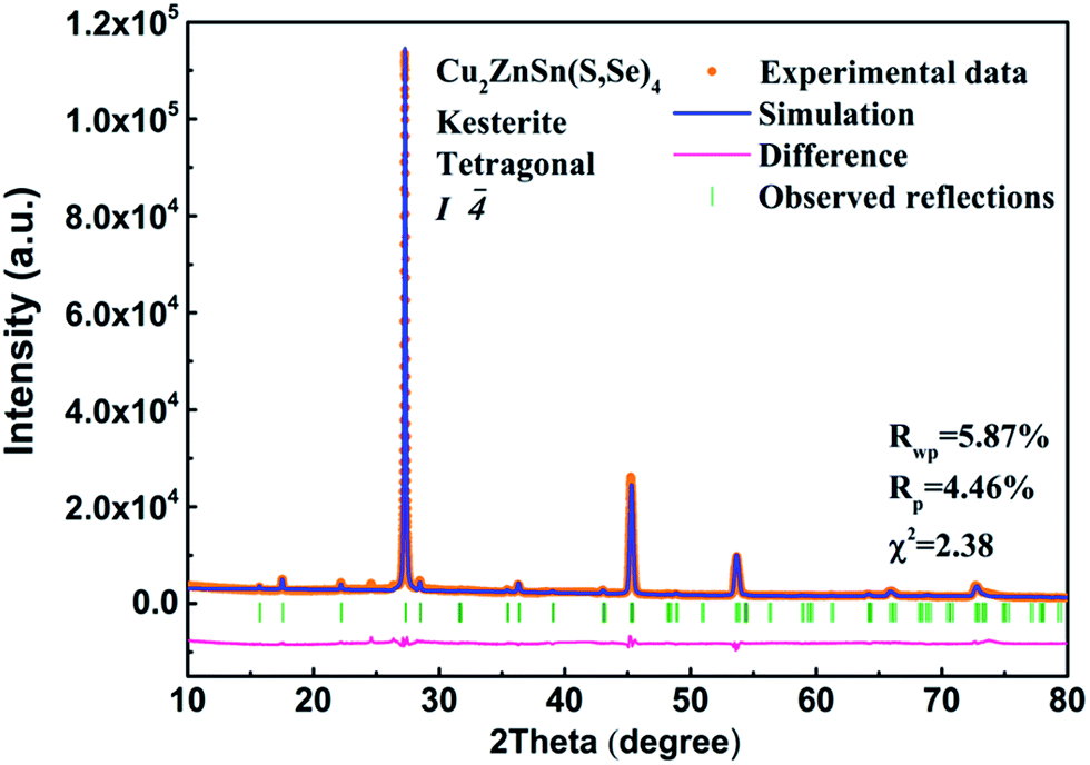 | ||
| Fig. 3 Rietveld refined X-ray diffraction profile of CZTSSe film, where the orange dots are experimental data, the blue line is the obtained fit, the green ticks are the Bragg peak positions of the kesterite-type structure, and the pink line is the difference between the experimental and calculated data. | ||
Reducing optical losses is an important way to increase the density of photo-generated carriers for PV devices. Therefore, an AR layer is usually adopted to realize the low reflectance of solar cells, such as MgF2, SiO2 and SiNx:H in CIGS and Si PV devices.31,32 Several reports have proven that Al2O3 can have good AR properties with wide thickness ranges for Si solar cells.33 To verify the AR performance of Al2O3 in CZTSSe solar cells, the reflectance spectra of CZTSSe with various thicknesses of Al2O3 thin films were obtained for wavelengths from 350 nm to 1250 nm, as shown in Fig. 4(a). A remarkable decrease in the total reflectance of CZTSSe with Al2O3 thin films can be observed over a wide spectral range. The spectrum-weighted average reflectance (Rave) can be defined as:34
 | (3) |
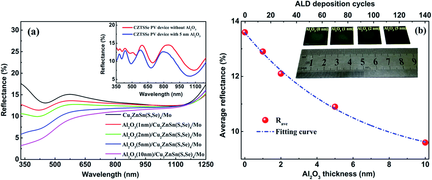 | ||
| Fig. 4 (a) The reflectance spectra of CZTSSe thin films without Al2O3 thin film and with Al2O3 thin film at various thicknesses. The inset is the reflectance spectra of CZTSSe solar cells without Al2O3 thin film and with 5 nm Al2O3 thin film. (b) The Rave of CZTSSe thin films coated with Al2O3 thin films as a function of Al2O3 thickness and ALD cycles. The inset is digital photographs of CZTSSe thin films with Al2O3 thin film at various thicknesses. | ||
Besides its AR properties, Al2O3 thin film can also provide an excellent passivation effect for both p- and n-type materials. In order to explore the origin of the passivation mechanism of Al2O3 on CZTSSe, the chemical states of Al and O were identified through XPS measurements. Fig. 5 shows the XPS spectra of Zn 2p, Al 2p and O 1s, respectively. The Zn 2p spectrum consists of two narrow peaks at 1022.5 eV and 1045.5 eV, corresponding to Zn 2p1/2 and 2p3/2, with a peak splitting of ΔE = 23.0 eV, in accordance with the standard splitting of 23 eV for Zn(II) state, as shown in Fig. 5(a).35 The O 1s core-level XPS spectra of Al2O3 thin film is shown in Fig. 5(b). The O 1s spectrum can be fitted into two peaks, located at 531.4 eV and 532.6 eV, which are attributed to Al–O–Al bonds and Al–OH bonds.33 The appearance of hydroxyl groups can be assigned to an incomplete reaction during eqn (1) and adsorbed H2O on the surface.36 Fig. 5(c) shows the Al 2p core-level XPS spectra of the as-deposited and annealed Al2O3 thin film. For the as-deposited sample, the Al 2p peak with a binding energy of 75.2 eV is assigned to the Al–O bond, which can be fitted into two subspectra located at 74.2 eV and 75.6 eV, corresponding to O–Al–O bonds and Al–OH bonds, respectively.35 After annealing, the component at 75.6 eV disappears, while the peak with a binding energy of 74.2 eV remains, indicating the disappearance of Al–OH bonds during the annealing process. According to previous literature, the residual O–H bonds would be broken easily to release interstitial O and interstitial H atoms during the annealing process.37 The interstitial H ions migrate through the Al2O3 matrix and arrive at the Al2O3/CZTSSe interface to passivate the dangling bonds or grain boundaries of the CZTSSe film.38 Meanwhile, the excess O ions released from hydroxyl groups are also helpful for the formation of O interstitials (Oi), which are responsible for the negative fixed charge in Al2O3 thin film, leading to the enhancement of field-effect passivation.37 Furthermore, negative fixed charge at the interface between CZTSSe and Al2O3 can effectively strengthen the built-in field of the p–n junction, which can enhance the carrier-separation efficiency.
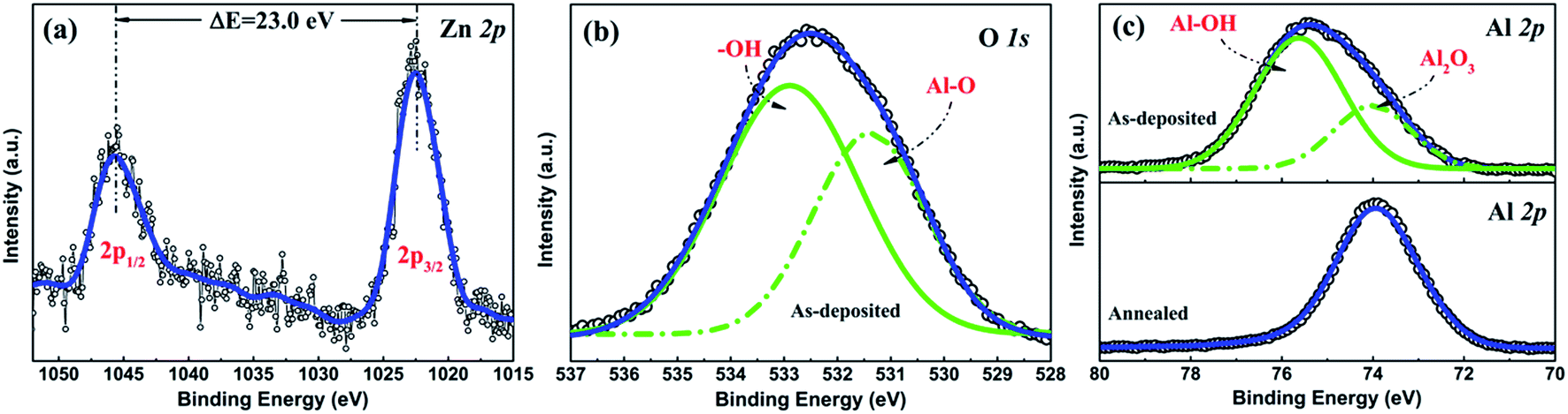 | ||
| Fig. 5 XPS spectra of (a) the Zn 2p core level of the CZTSSe film, (b) the O 1s core level of as-deposited Al2O3, and (c) the Al 2p core-level of as-deposited and annealed Al2O3. | ||
To further understand the effects of passivation on device performance, the photovoltaic investigation of CZTSSe solar cells with the structure SLG/Mo/CZTSSe/Al2O3/CdS/i-ZnO/ITO/Al was carried out. Fig. 6 displays current density–voltage (J–V) curves for CZTSSe solar cells with various thicknesses of Al2O3 under standard AM 1.5 illumination (100 mW cm−2). The detailed device parameters are listed in Table 1. It was found that the unpassivated CZTSSe solar cell achieved a PCE of 2.24%, and the Voc, Jsc and FF values are 0.262 V, 21.42 mA cm−2 and 38.22%, respectively. After Al2O3 deposition, the PCE increased sharply and then decreased with increasing Al2O3 thickness from 1 nm to 5 nm. The PCE reached the highest value of 5.66% at a film thickness of 2 nm. The Voc, Jsc and FF change similarly to the PCE, revealing the highest values of 0.361 V, 33.78 mA cm−2 and 48.98%, respectively. Compared with CZTSSe solar cells without Al2O3 passivation, the Voc, Jsc and FF values of the CZTSSe with 2 nm Al2O3 thin film were increased by 37.8%, 57.8% and 28.2%, respectively. This improvement in device performance can be assigned to the AR performance of Al2O3 thin film and the reduction of the density of acceptor-like states at the interface between CZTSSe/Al2O3, resulting in the decreased compensation of photo-generated carriers.13
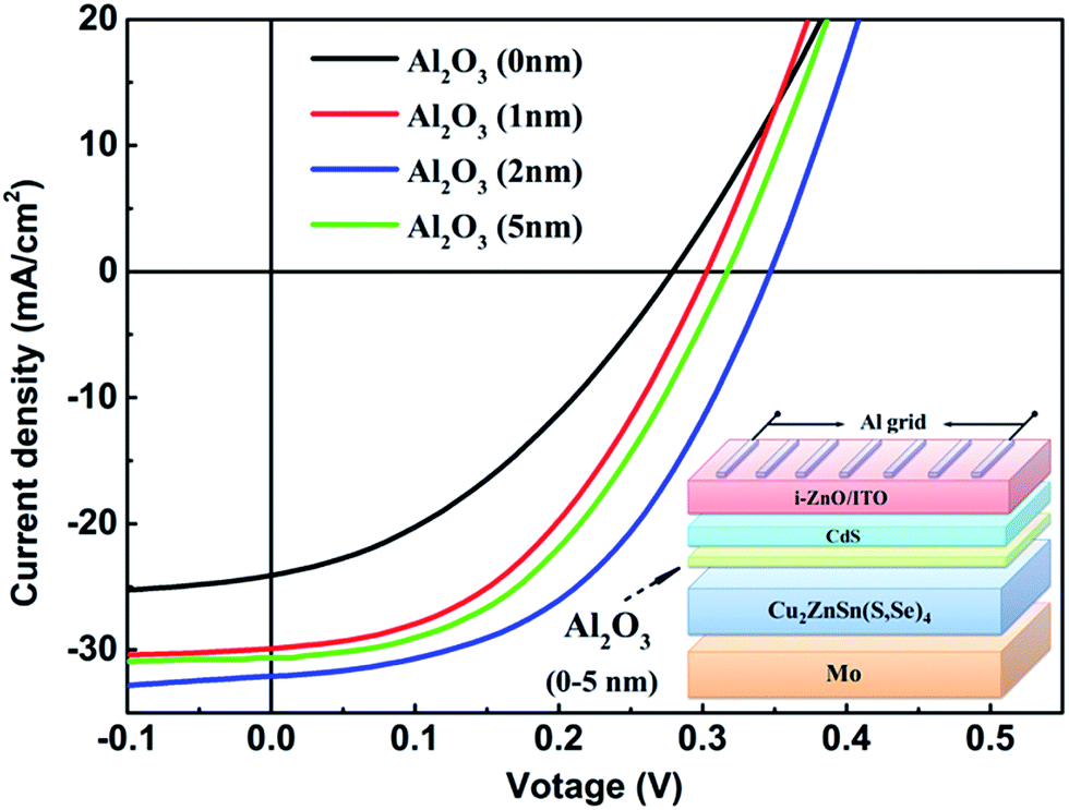 | ||
| Fig. 6 Current–voltage curves for CZTSSe solar cells with Al2O3 thin film at various thicknesses, in comparison with unpassivated CZTSSe solar cells. The inset is the schematic of the device structure. | ||
| Al2O3 thickness (nm) | Voc (V) | Jsc (mA cm−2) | FF (%) | Eff. (%) |
|---|---|---|---|---|
| 0 | 0.262 | 21.42 | 38.22 | 2.24 |
| 1 | 0.301 | 26.84 | 39.45 | 3.12 |
| 2 | 0.361 | 33.78 | 48.98 | 5.66 |
| 5 | 0.312 | 30.68 | 46.14 | 4.39 |
| 10 | — | — | — | — |
Fig. 7(a) displays the EQE spectra of CZTSSe solar cells with various thicknesses of Al2O3 passivation layers. For comparison, a CZTSSe solar cell without an Al2O3 passivation layer is also added as a reference. All of the CZTSSe solar cells present a distinct spectral response, and with increasing Al2O3 thickness, the EQE value shows a similar trend to that of the PCE results. The CZTSSe solar cell with 2 nm Al2O3 exhibits the highest value of around 80% in the wavelength region of 500 nm to 900 nm. It is found that the EQE is improved at all wavelengths with increasing Al2O3 thickness, especially in the long wavelength region. The improvement in EQE indicates the improvement in the collection length of photo-generated carriers, which is due to the passivation of the CZTSSe surface and/or grain boundaries by Al2O3 films.24 In addition, the bandgap of the CZTSSe films is determined by plotting [E × ln(1 − EQE)]2 versus E using the EQE spectra of the CZTSSe solar cell, as shown in Fig. 7(b). It is found that the bandgaps of all of the CZTSSe films have the value of 1.07 eV, which indicates that the ALD process has no influence on the stoichiometric ratio of the CZTSSe film, especially the S/Se ratio, which is consistent with the XPS and EDS results. Therefore, it is deduced that the improvement of the performance of CZTSSe solar cells mainly originates from decreases in the reflectance of CZTSSe and the surface passivation of Al2O3.
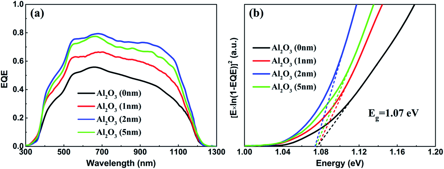 | ||
| Fig. 7 (a) EQE spectra of CZTSSe solar cells with Al2O3 thin film at various thicknesses. (b) Band gap values of CZTSSe solar cells, with Al2O3 thin film at various thicknesses, determined by the [E × ln(1 − EQE)]2 vs. E curve. | ||
Based on the above discussions, it can be concluded that the development of CZTSSe solar cells originates from two aspects. On one hand, the deposition of Al2O3 thin films can reduce the reflectance of CZTSSe films and increase photo-generated carriers, leading to an improvement in device performance, especially the Jsc value. On the other hand, Al2O3 thin films can not only saturate the defects and dangling bonds at the interface between CZTSSe and CdS, but also produce a large amount of negative fixed charge to reduce interface recombination and increase the carrier separation efficiency, resulting in an increased Voc value. In addition, although thicker Al2O3 thin films are beneficial for obtaining lower reflectance for the CZTSSe films, the optimal CZTSSe PV device was obtained at the Al2O3 thickness of 2 nm in the present work, which can be explained as follows. According to our results and other literature on Si and CIGS solar cells, a thicker passivation layer causes reduction in the fixed charge, leading to the debasing of field-effect passivation. Therefore, the Al2O3 passivation layer should be kept thin enough so that the photo-excited electrons are able to effectively tunnel through the layer in the device.
4. Conclusions
In summary, Al2O3 thin films of various thicknesses were deposited on the top of CZTSSe prior to CdS deposition by ALD. The influence of the thickness of Al2O3 thin films on the reflectance and PCE values of CZTSSe solar cells was investigated in detail. The CZTSSe without the Al2O3 thin film achieved an Rave of 13.6%. After deposition of the Al2O3 thin films, the Rave values of CZTSSe films with 1 nm, 2 nm, 5 nm and 10 nm Al2O3 were 12.9%, 12.1%, 10.9% and 9.6%, respectively. This decrease in Rave demonstrates that Al2O3 thin films can provide favorable AR properties. The XPS results indicate the existence of a large amount of Oi, which is believed to be the origin of field effect passivation caused by the negative fixed charge. The appearance of Oi can not only provide field effect passivation to depress surface recombination, but also enhance the built-in field of the p–n junction to increase the carrier-separation efficiency. The Voc, Jsc, and η of CZTSSe solar cells with 2 nm Al2O3 thin film achieved the highest values of 0.361 V, 33.78 mA and 5.66%, respectively, in comparison with 0.262 V, 21.42 mA and 2.24% for the CZTSSe solar cell without passivation.Conflicts of interest
There are no conflicts to declare.Acknowledgements
This work was financially supported by the National Natural Science Foundation of China (Grant No. 61604029 and 61774075) and the Fundamental Research Funds for the Central Universities (Grant No. DUT18LK48).References
- P. Jackson, D. Hariskos, R. Wuerz, O. Kiowski, A. Bauer, T. M. Friedlmeier and M. Powalla, Phys. Status Solidi RRL, 2015, 9, 28–31 CrossRef.
- P. Jackson, R. Wuerz, D. Hariskos, E. Lotter, W. Witte and M. Powalla, Phys. Status Solidi RRL, 2016, 10, 583–586 CrossRef.
- N. Shibayama, Y. W. Zhang, T. Satake and M. Sugiyama, RSC Adv., 2017, 7, 25347–25352 RSC.
- Z. Y. Xiao, B. Yao, Y. F. Li, Z. H. Ding, Z. M. Gao, H. F. Zhao, L. G. Zhang, Z. Z. Zhang, Y. R. Sui and G. Wang, ACS Appl. Mater. Interfaces, 2016, 8, 17334–17342 Search PubMed.
- S. Y. Chen, A. Walsh, X. G. Gong and S. H. Wei, Adv. Mater., 2013, 25, 1522–1539 CrossRef PubMed.
- A. Walsh, S. Y. Chen, S. H. Wei and X. G. Gong, Adv. Energy Mater., 2012, 2, 400–409 CrossRef.
- J. Kim, H. Hiroi, T. K. Todorov, O. Gunawan, M. Kuwahara, T. Gokmen, D. Nair, M. Hopstaken, B. Shin, Y. S. Lee, W. Wang, H. Sugimoto and D. B. Mitzi, Adv. Mater., 2014, 26, 7427–7431 CrossRef PubMed.
- D. B. Mitzi, O. Gunawan, T. K. Todorov, K. Wang and S. Guha, Sol. Energy Mater. Sol. Cells, 2011, 95, 1421–1436 CrossRef.
- K. Ramasamy, M. A. Malik and P. O’Brien, Chem. Commun., 2012, 48, 5703–5714 RSC.
- Q. Tian, Y. Cui, G. Wang and D. Pan, RSC Adv., 2015, 5, 4184–4190 RSC.
- Z.-Y. Xiao, Y.-F. Li, B. Yao, Z.-H. Ding, R. Deng, H.-F. Zhao, L.-G. Zhang and Z.-Z. Zhang, RSC Adv., 2015, 5, 103451–103457 RSC.
- W. Wang, M. T. Winkler, O. Gunawan, T. Gokmen, T. K. Todorov, Y. Zhu and D. B. Mitzi, Adv. Energy Mater., 2014, 4, 1301465 CrossRef.
- S. Ahmed, K. B. Reuter, O. Gunawan, L. Guo, L. T. Romankiw and H. Deligianni, Adv. Energy Mater., 2012, 2, 253–259 CrossRef.
- M. E. Erkan, V. Chawla and M. A. Scarpulla, J. Appl. Phys., 2016, 119, 194504 CrossRef.
- G. Sozzi, S. D. Napoli, R. Menozzi, B. Bissig, S. Buecheler and A. N. Tiwari, Sol. Energy Mater. Sol. Cells, 2017, 165, 94–102 CrossRef.
- K. Herz, A. Eicke, F. Kessler, R. Wachter and M. Powalla, Thin Solid Films, 2003, 431, 392–397 CrossRef.
- B. A. Chambers, G. G. Andersson, J. S. Quinton, J. Jasieniak, B. I. MacDonald, M. Ionescu, A. Deslandes, J. S. Quinton, J. J. Jasieniak and G. G. Andersson, Sol. Energy Mater. Sol. Cells, 2014, 125, 164–169 CrossRef.
- R. Kotipalli, B. Vermang, J. Joel, R. Rajkumar, M. Edoff and D. Flandre, AIP Adv., 2015, 5, 107101 CrossRef.
- J. Löckinger, S. Nishiwaki, T. P. Weiss, B. Bissig, Y. E. Romanyuk, S. Buecheler and A. N. Tiwari, Sol. Energy Mater. Sol. Cells, 2018, 174, 397–404 CrossRef.
- S. Gatz, T. Dullweber, V. Mertens, F. Einsele and R. Brendel, Sol. Energy Mater. Sol. Cells, 2012, 96, 180–185 CrossRef.
- W.-C. Wang, M. C. Tsai, J. Yang, C. Hsu and M.-J. Chen, ACS Appl. Mater. Interfaces, 2015, 7, 10228–10237 Search PubMed.
- L. Q. Zhu, Q. Fang, X. J. Wang, J. P. Zhang, M. Liu, G. He and L. D. Zhang, Appl. Surf. Sci., 2008, 254, 5439–5444 CrossRef.
- G. L. Lu, F. Zheng, J. Q. Wang and W. Z. Shen, Prog. Photovoltaics, 2017, 25, 280–290 Search PubMed.
- P. Casper, R. Hünig, G. Gomard, O. Kiowski, C. Reitz, U. Lemmer, M. Powalla and M. Hetterich, Phys. Status Solidi RRL, 2016, 10, 376–380 CrossRef.
- W.-W. Hsu, J. Y. Chen, T.-H. Cheng, S. C. Lu, W.-S. Ho, Y.-Y. Chen, Y.-J. Chien and C. W. Liu, Appl. Phys. Lett., 2012, 100, 023508 CrossRef.
- P. Poodt, A. Lankhorst, F. Roozeboom, K. Spee, D. Maas and A. Vermeer, Adv. Mater., 2010, 22, 3564–3567 CrossRef PubMed.
- N. M. Terlinden, G. Dingemans, M. C. M. Van de Sanden and W. M. M. Kessels, Appl. Phys. Lett., 2010, 96, 112101 CrossRef.
- L. Meng, B. Yao, Y. F. Li, Z. H. Ding, Z. Y. Xiao, K. S. Liu and G. Wang, J. Alloys Compd., 2017, 710, 403–408 CrossRef.
- K. Wang, B. Shin, K. B. Reuter, T. Todorov, D. B. Mitzi and S. Guha, Appl. Phys. Lett., 2011, 98, 051912 CrossRef.
- S. W. Shin, J. H. Han, Y. C. Park, G. L. Agawane, C. H. Jeong, J. H. Yun, A. V. Moholkar, J. Y. Lee and J. H. Kim, J. Mater. Chem., 2012, 22, 21727 RSC.
- H.-J. Jeong, Y.-C. Kim, S. K. Lee, Y. Jeong, J.-W. Song, J.-H. Yun and J.-H. Jang, ACS Appl. Mater. Interfaces, 2017, 9, 25404–25411 Search PubMed.
- S.-Y. Han, C. Q. Pan, D.-H. Kim and C.-H. Chang, RSC Adv., 2015, 5, 24712–24717 RSC.
- L. Q. Zhu, Y. H. Liu, H. L. Zhang, H. Xiao and L. Q. Guo, Appl. Surf. Sci., 2014, 288, 430–434 CrossRef.
- P. Menna, G. Di Francia and V. La Ferrara, Sol. Energy Mater. Sol. Cells, 1995, 37, 13–24 CrossRef.
- Y. T. Qu, G. Zoppi and N. S. Beattie, Prog. Photovoltaics, 2016, 24, 836–845 Search PubMed.
- C. Van der Marel, M. Yildirim and H. R. Stapert, J. Vac. Sci. Technol., A, 2005, 23, 1456 Search PubMed.
- V. Naumann, M. Otto, R. B. Wehrspohn, M. Werner and C. Hagendorf, Energy Procedia, 2012, 27, 312–318 CrossRef.
- Y.-W. Cheng, F.-L. Tang, H.-T. Xue, H.-X. Liu and B. Gao, Appl. Surf. Sci., 2017, 394, 58–62 CrossRef.
| This journal is © The Royal Society of Chemistry 2018 |