DOI:
10.1039/C8RA03398F
(Paper)
RSC Adv., 2018,
8, 25514-25518
A vertical WSe2–MoSe2 p–n heterostructure with tunable gate rectification†
Received
20th April 2018
, Accepted 4th July 2018
First published on 17th July 2018
Abstract
Here, we report the synthesis of a vertical MoSe2/WSe2 p–n heterostructure using a sputtering-CVD method. Unlike the conventional CVD method, this method produced a continuous MoSe2/WSe2 p–n heterostructure. WSe2 and MoSe2 back-gated field effect transistors (FETs) exhibited good gate modulation behavior, and high hole and electron mobilities of ∼2.2 and ∼15.1 cm2 V−1 s−1, respectively. The fabricated vertical MoSe2/WSe2 p–n diode showed rectifying I–V behavior with back-gate tunability. The rectification ratio of the diode was increased with increasing gate voltage, and was increased from ∼18 to ∼1600 as the gate bias increased from −40 V to +40 V. This is attributed to the fact that the barrier height between p-WSe2 and n-MoSe2 is modulated due to the back-gate bias. The rectification ratio is higher than the previously reported values for the TMDC p–n heterostructure grown by CVD.
1. Introduction
The two-dimensional transition metal dichalcogenides (TMDCs), in the form of MX2 (M = metal and X = S, Se or Te), have recently received much attention for the study of physics in 2D materials and in layered structures.1–3 In TMDCs, each M-atom (transition metal element) layer is enclosed within two X-atom (chalcogen element) layers and the atoms in the layers have hexagonally packed structures.1,3,4 Every X–M–X atom arrangement is held together by van der Waals interactions. And due to the weak van der Waals interactions of each layer, it is possible to tune the band structure of the X–M–X atoms from an indirect (∼1.2 eV) to a direct band gap (∼2.5 eV) through heterogeneous integration. TMDCs exhibit good electrical properties1,3,5,6 with high on/off ratios of ∼108, and room-temperature mobility over 200 cm2 V−1 s−1.7–11 Due to weak van der Waals forces between each stacking layer, 2D heterostructures can be easily produced by using mechanical transfer methods. Since p–n junctions are basic building blocks for electronic devices, and other optoelectronic devices,12–14 the implementation of homo or hetero p–n junctions is a key interest among researchers. Mechanical exfoliation is an easy way to produce p–n junctions; however, it is not suitable for mass production. Recently, many efforts have been made to apply chemical vapor deposition (CVD) to 2D heterostructures such as MoS2/graphene,15 WS2/MoS2,16 WS2/h-BN,17 and n-MoS2/p-WSe2,18 MoSe2–WSe2.18 Nonetheless, the current rectification behavior of CVD-grown TMDC heterostructures is rarely reported and is poor.18 Our group has been focusing on the synthesis of TMDCs by a sputtering-CVD method.19,20 In this paper, we report a MoSe2/WSe2 p–n heterostructure. A W film was sputtered and then selenized to form WSe2, and Mo was sputtered on the WSe2 and selenized to form a vertical MoSe2 (n)/WSe2 (p) junction. Unlike the conventional CVD method, this method produces a continuous MoSe2/WSe2 film. The WSe2 and MoSe2 back-gate field effect transistors (FETs) exhibited good gate modulation behavior, and high hole and electron mobilities of ∼2.2 and ∼15.1 cm2 V−1 s−1, respectively. The fabricated MoSe2/WSe2 p–n diodes showed rectifying I–V behavior, and the forward diode current increased with increasing back-gate bias. The p–n diode with back-gate tunability showed a high gate-tunable rectification ratio varying from ∼18 to ∼1600 at different back-gate biases. This can be attributed to the fact that the barrier height between p-WSe2 and n-MoSe2 is modulated due to the back-gate bias. The rectification ratio is much higher than the previously reported value for the TMDC p–n heterostructure (MoS2/WSe2) grown by CVD.18
2. Experimental details
2.1 Synthesis of MoSe2/WSe2
Fig. 1 illustrates the overall growth scheme for the vertical MoSe2/WSe2 heterostructure. The MoSe2/WSe2 films were prepared by a RF magnetron sputtering system combined with a selenization process, using a W (99.9% pure) and a Mo (99.9% pure) target in an argon environment at room temperature. Initially a W thin film with a desired thickness was sputtered on a SiO2/Si substrate through a metal shadow mask. Before sputtering, the chamber was evacuated by a turbomolecular pump to a vacuum at ∼2 × 10⁻⁶ Torr. During the film deposition, the Ar gas was maintained at 10 sccm, and the power was fixed at 150 W with a deposition time of 1200 s. Subsequently, the as-deposited W film was further put in the center of a furnace for selenization at 650 °C for 30 min to form a WSe2 film. The heating area for the selenium evaporation was fixed at 270 °C. The amount of selenium powder (0.5–0.8 g) used and the flow of Ar as a carrier gas were fixed for all the experiments. After the growth of the WSe2, a Mo film was deposited on it. The sputtering conditions were the same for both films (W & Mo). The Mo/WSe2 film was again placed in the tube furnace for selenization annealing to form the MoSe2/WSe2 heterojunction. The p–n junction area was defined by overlapped regions of two layers (Fig. 1). After the formation of the active area, Al (100 nm) was deposited on the top via e-beam evaporation.
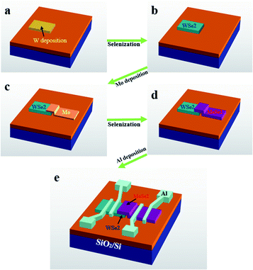 |
| | Fig. 1 Schematic of the MoSe2/WSe2 heterostructure. (a) W was deposited onto the SiO2/Si substrate. (b) A WSe2 film was formed via selenization. (c) Molybdenum (Mo) was deposited on the top of the WSe2. (d) A MoSe2/WSe2 heterostructure was formed via selenization. (e) The MoSe2/WSe2 heterostructure with Al electrodes. | |
2.2 Characterization techniques
All the samples were characterized using the latest analytical characterization techniques. WSe2, MoSe2 and MoSe2/WSe2 heterostructure films were analyzed by using a Renishaw inVia RE04, with a 514 nm Ar laser, a laser spot-size of 1 μm, laser power of 10 mW, and an exposure time of 30 s. A Si substrate with a Raman peak of 520 cm−1 was used for calibration. X-ray photoelectron spectroscopy (XPS) (PHI 5000 Versa Probe, 25 W Al Kα, 6.7 × 10⁻⁸ Pa) was used for binding energy and elemental composition analysis. The crystallinity of the film was examined using in-plan X-ray diffraction (XRD, Rigaku) with Cu-Kα radiation (λ = 54![[thin space (1/6-em)]](https://www.rsc.org/images/entities/char_2009.gif) 178 Å) operated at 50 kV and 300 mA current. FE-SEM (HITACHI S-4700) was used to demonstrate the morphological nature of the WSe2, MoSe2 and MoSe2/WSe2 heterostructure films. The crystal structures of the resulting products were analysed using a JEOL-2010F TEM with the assistance of Gatan Digital Micrograph software (Gatan Microscopy Suite 2.0) for image acquisition and processing (FFT, R-FFT, etc.).
178 Å) operated at 50 kV and 300 mA current. FE-SEM (HITACHI S-4700) was used to demonstrate the morphological nature of the WSe2, MoSe2 and MoSe2/WSe2 heterostructure films. The crystal structures of the resulting products were analysed using a JEOL-2010F TEM with the assistance of Gatan Digital Micrograph software (Gatan Microscopy Suite 2.0) for image acquisition and processing (FFT, R-FFT, etc.).
3. Results and discussion
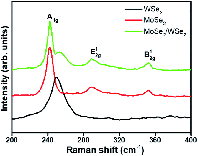
Raman spectroscopy was used to characterize the formation of WSe2, MoSe2 and the MoSe2/WSe2 heterostructures. For the WSe2 film, one main characteristic peak at 250.5 cm−1, assigned to the E12g mode was observed.21 On the other hand, for the MoSe2 film three characteristic phonon modes appeared in the Raman spectra: a sharp one at low wavenumber (∼242.2 cm−1) associated with the out-of-plane vibration of Se atoms, and two broad ones at higher wavenumber (∼290.1 cm−1), (∼352.0 cm−1) corresponding to the E12g and B12g modes associated with the in-plane vibration of Mo and Se atoms.22–24 In the Raman spectrum of the MoSe2/WSe2 heterostructure, peaks corresponding to both WSe2 and MoSe2 films appeared. In addition, there was no significant shift of the representative peaks for WSe2 and MoSe2 in the heterostructure. This supports that there was no serious alloying process of the WSe2 and MoSe2 encountered in the synthetic procedure, since the alloying process would be accompanied by peak shifts (Fig. 2).18
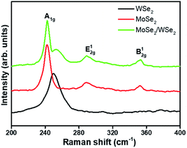 |
| | Fig. 2 Raman spectra of WSe2, MoSe2 and the MoSe2/WSe2 heterostructure films. | |
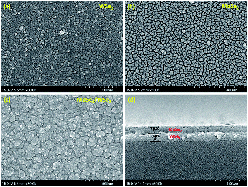
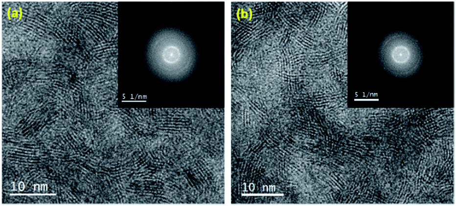
Scanning electron microscope (SEM) images reveal the formation of homogeneous MoSe2 and WSe2 thin films (Fig. 3a and b). Further, SEM confirms the existence of a dense array of grains for the MoSe2/WSe2 heterostructure (Fig. 3c). The thicknesses of the MoSe2 and WSe2 films were ∼160 nm and ∼140 nm, respectively, estimated from the cross-sectional SEM image (Fig. 3d). The elemental mapping images of W, Mo and Se elements for the MoSe2/WSe2 heterostructure are provided in the ESI in Fig. S1.† Transmission electron microscopy (TEM) characterization was further performed to analyse the surface of the MoSe2/WSe2 heterostructure as shown in Fig. 4. The TEM images revealed that the film surface consisted of highly dense layers with a polycrystalline edge-exposed site structure.
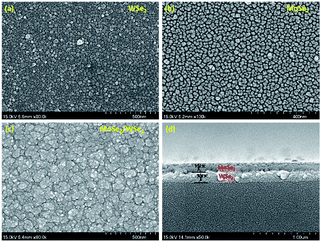 |
| | Fig. 3 Top-down and cross-sectional SEM images. Top-down images of (a) WSe2, (b) MoSe2 and (c) the MoSe2/WSe2 heterostructure (d) cross-sectional image. | |
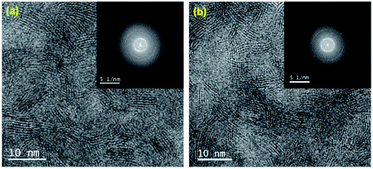 |
| | Fig. 4 (a and b) TEM images of the MoSe2/WSe2 heterostructure. | |
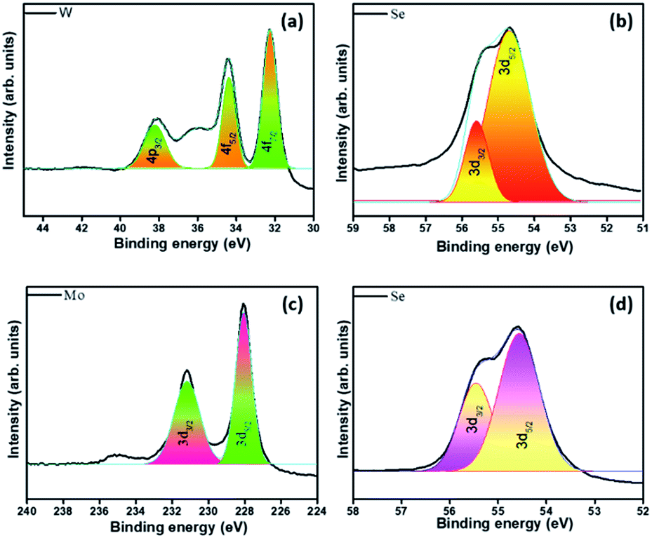
X-ray photoelectron spectroscopy (XPS) was applied to examine the binding energies of WSe2, MoSe2 and the MoSe2/WSe2 heterostructure (Fig. 5a–d). The complete survey scans of WSe2 and MoSe2 are provided in Fig. S2.† From the WSe2 film, the peaks at 32.2 and 34.4 eV were assigned to the doublet W 4f7/2 and W 4f5/2 binding energies, respectively and the peak at 38 eV was assigned to W 5p3/2 binding energy. The Se peaks at 54.7 and 55.1 eV (Fig. 5a and b) were indexed to be Se 3d5/2 and Se 3d3/2 respectively.21,25 For the MoSe2 film, Mo 3d3/2 and 3d5/2 core levels peaks were located at 231.1 and 228.0 eV, respectively. The peak of Se around 54.0 eV can be divided into Se 3d5/2 and Se 3d3/2 with peak positions at 54.6 and 55.2 eV, respectively26,27 (Fig. 5c and d). The XPS survey scan of the MoSe2/WSe2 heterostructure revealed the presence of W, Mo and Se elements (Fig. S3†).
 |
| | Fig. 5 XPS spectra: (a) W 4f and (b) Se 3d binding energies for WSe2. (c) Mo 3d, 4f and (d) Se 3d binding energies for MoSe2. | |
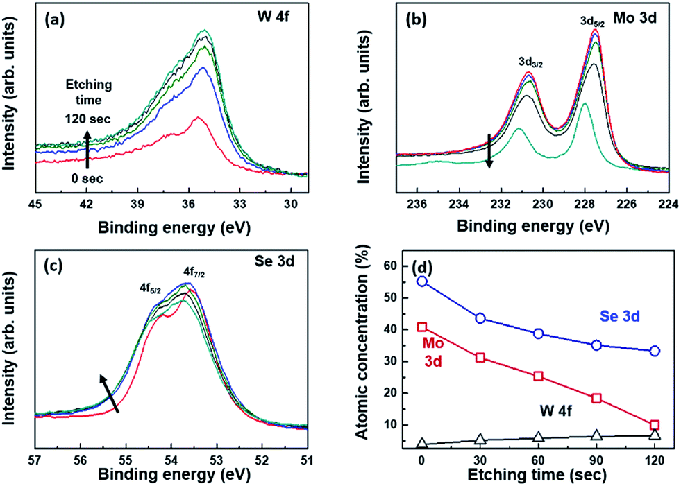
XPS depth profile analysis was performed to investigate the typical WSe2/MoSe2 heterostructure. A 1 keV Ar ion beam was used for continuous etching of the WSe2/MoSe2 heterostructure in the direction from top to bottom. Fig. 6a–c show the XPS depth profile spectra for the W, Mo and Se binding energies. The Mo peak intensities were decreased and the W peak intensities were increased with etching time, whereas Se peak intensities were slightly varied due to the presence of Se in both structures. These findings confirm the heterostructure formation without diffusion or alloy formation. The Mo atomic concentration from the top-layer of MoSe2 drastically decreased, although the W atomic concentration from the bottom-layer of WSe2 linearly increased up to 120 s of etching time as shown in Fig. 6d. The cross sectional SEM image of the heterostructure is also evidence of our dual layered structure.
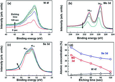 |
| | Fig. 6 XPS depth profile spectra of (a) W 4f, (b) Mo 3d, and (c) Se 3d binding energies and (d) their atomic concentration variations in terms of etching time for the MoSe2/WSe2 heterostructure. | |
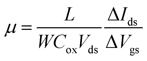
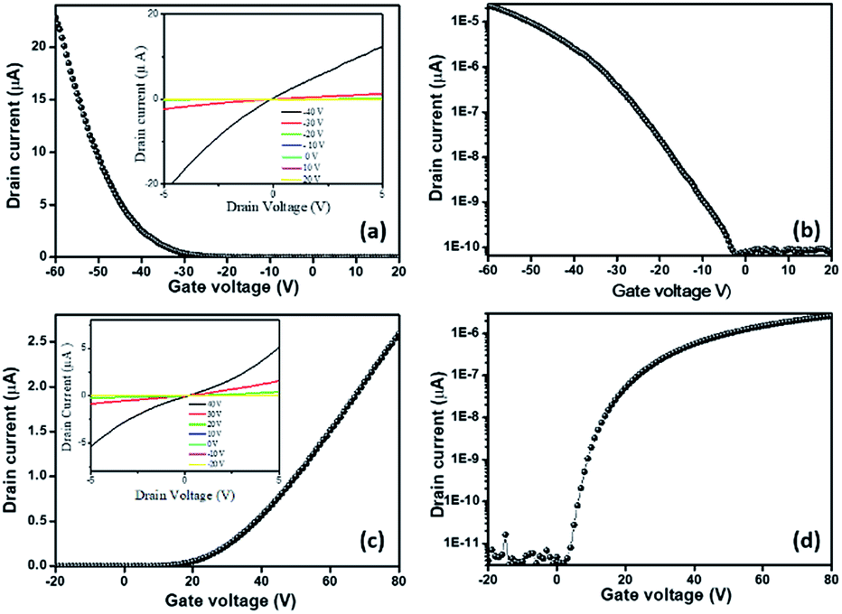
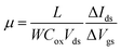
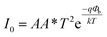
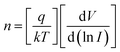
We characterized the electrical transport properties of WSe2 and MoSe2 back-gated field effect transistor (FET) devices (Fig. 7a and b). Transfer characteristics of source-drain current (Ids) versus back-gate voltage (Vgs) were measured for WSe2 and MoSe2 FETs. The WSe2 and MoSe2 devices presented p-type and n-type behavior under back-gate biasing (constant bias, Vds = 1 V), respectively, similar to the earlier reports by other research group.22,28 The field-effect mobility was extracted from the slope of ΔIds/ΔVgs fitted to the linear region of the transfer curves using the following equation
| |
 | (1) |
where
W is the width of the channel (10 μm),
L is the length of the channel (10 μm),
Cox is the capacitance per unit area of the gate dielectric with 300 nm thickness (1.15 × 10
−8 F cm
−1),
Vds is the applied drain voltage and Δ
Ids/Δ
Vgs is the slope of the linear part of the transfer plot (
Ids–
Vgs) or the transconductance. The estimated field-effect mobility values of WSe
2 and MoSe
2 FETs are ∼2.2 cm
2 V
−1 s
−1 and ∼15.1 cm
2 V
−1 s
−1, respectively and on/off current ratios are ∼3–6 × 10
5. The linear
Ids–
Vds characteristics of both WSe
2 and MoSe
2 devices exhibited good ohmic contacts and there was an absence of significant charge injection barriers. Compared to the subthreshold characteristics, MoSe
2 had a better subthreshold swing than WSe
2. Electrical properties of the MoSe
2/WSe
2 heterostructure film were also measured. Voltages were applied to the metal pads of the p-type WSe
2 and the n-type MoSe
2 with changing back-gate bias.
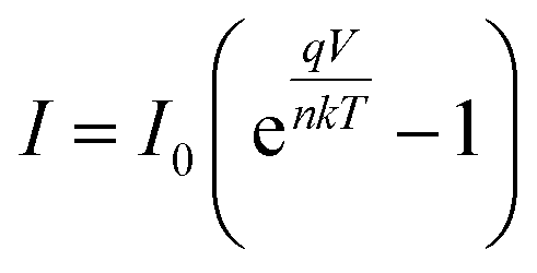
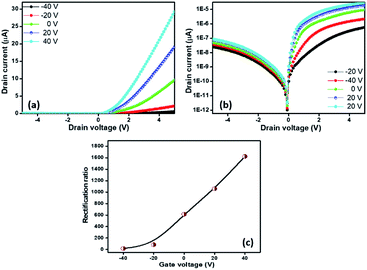
Fig. 8a shows the linear
I–
V curves of the stacked MoSe
2/WSe
2 p–n junction at various back-gate voltages. The drain voltage in
Fig. 8a is the voltage applied to p-WSe
2 with respect to n-MoSe
2. Rectifying
I–
V characteristics were observed from the p–n junction between n-type MoSe
2 and p-type WSe
2. The current in Schottky barrier diodes can be expressed as
| |
 | (2) |
where,
I0 is the saturation current,
k is the Boltzmann constant,
T is the absolute temperature,
q is the elementary electric charge, and
V is the applied voltage. The saturation current
I0 is expressed as
| |
 | (3) |
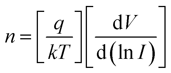
where,
A is the device area,
A* is the effective Richardson constant, and
Φb is the barrier height. The ideality factor of the Schottky diode is extracted from the slope of the linear region of the ln
I–
V characteristic and is expressed as
| |
 | (4) |
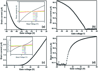 |
| | Fig. 7 Electrical output and transfer curves of theWSe2 and MoSe2 devices. (a and b) Id–Vg of the WSe2 FET at fixed Vgs = 1 V; Ids–Vds of the WSe2 FET at Vds: 20 V to −40 V (inset). (c and d) Ids–Vgs of the MoSe2 FET at Vgs = 1 V; Ids–Vds of the MoSe2 FET at Vds: 20 V to −40 V (inset). | |
 |
| | Fig. 8 Linear scale and log scale plots of I–V characteristics of the MoSe2/WSe2 heterojunction (a) linear scale plots of I–V. (b) Log scale I – linear V with different back-gate voltages Vgs (c) rectification ratio (Ids@Vds = 1 V/Ids@Vds = −1 V) as a function of back-gate voltage Vgs. | |
The ideality factor varies with back-gate bias, and is ∼1.5 at a low bias range at Vgs = 40 V. The forward current is also increased upon increasing the back-gate voltage. The back-gate voltage controls the charge carrier densities of the electrons and holes in n-MoSe2 and p-WSe2. Since the bottom layer is p-type WSe2 and the top layer is n-type MoSe2, it is expected that hole concentration in WSe2 decreases with increasing back-gate bias, while the top n-type MoSe2 is less affected. Since the p–n junction is mainly composed of a vertical n-MoSe2/p-WSe2 junction and partly of a lateral side junction (the vertical junction area is much larger than the lateral side junction), the carrier concentration in the p-WSe2 layer is readily modulated by the back-gate bias, while the electrons in the top MoSe2 is less affected by screening due to the bottom WSe2 layer. Therefore, upon increasing the back-gate bias, the barrier height between WSe2 and MoSe2 decreases, and in turn increases the forward current. Fig. 8b is a plot of logarithmic I versus linear V.
The reverse current also increases with increasing back-gate voltage. This is also due to the lowered barrier height between p-WSe2 and n-MoSe2. Fig. 8c shows the rectification ratios of the diode. The rectification ratio is defined as the forward current at 1 V anode bias (the p-WSe2 voltage with respect to the n-MoSe2 voltage) versus reverse current at −1 V anode bias. It is observed that the rectification is modulated by the back-gate voltage. The rectification ratio of the diode is increased from ∼20 to ∼1800 as the back-gate bias is varied from −40 V to +40 V as shown in Fig. 8c. This value is much higher than the reported value (∼150) for the TMDC p–n heterostructure (MoS2/WSe2) grown by CVD.18
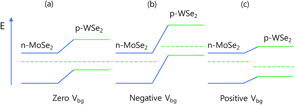
The energy band diagram (Fig. 9) reveals the formation of a built-in potential in the heterojunction p-WSe2/n-MoSe2, in which the conduction band (Ec) of WSe2 lies above that of MoSe2. The built-in potential is produced due to the formation of a depletion region at the interface. This barrier height is increased at negative gate bias as energy levels in WSe2 are shifted towards higher energy levels (Fig. 9b). Current is increased when the positive gate bias is applied (Fig. 9c). Positive gate bias leads to a decrease of the electron barrier and the energy levels in WSe2 shift towards lower energy, which results in the reduction of the barrier between the p- and n-regions and increased the forward current.
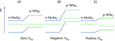 |
| | Fig. 9 Energy band diagram of n-MoSe2 and p-WSe2 at (a) 0, (b) negative and (c) positive back-gate voltage. | |
4. Conclusions
We fabricated a MoSe2/WSe2 p–n heterostructure using a sputtering-CVD method. The WSe2 and MoSe2 back-gated field effect transistors (FETs) exhibited good gate modulation behavior, and high hole and electron mobilities of ∼2.2 and ∼15.1 cm2 V−1 s−1, respectively. The fabricated MoSe2/WSe2 p–n diodes exhibited gate-tunable rectifying I–V characteristics. The rectification ratio of the p–n diode is increased with an increase in the gate voltage, and it is increased from ∼18 to ∼1600 as the gate bias is increased from −40 V to +40 V. This is attributed to the fact that the barrier height between p-WSe2 and n-MoSe2 is lowered due to the back-gate bias. The rectification ratio is much higher than the previously reported value for the TMDC p–n heterostructure (MoS2/WSe2) grown by CVD.
Conflicts of interest
There are no conflicts to declare.
Acknowledgements
This research was supported by the Basic Science Research Program and the Nano Material Technology Development Program through the National Research Foundation of Korea (NRF), and was funded by the Ministry of Education (2010-0020207, NRF-2016R1D1A1B01015047, 2018044021), and the Ministry of Science, ICT and Future Planning (NRF-2015M3A7B7045194, 2016M3A7B4909942).
Notes and references
- G.-B. Liu, D. Xiao, Y. Yao, X. Xu and W. Yao, Chem. Soc. Rev., 2015, 44, 2643–2663 RSC.
- M. Chhowalla, H. S. Shin, G. Eda, L.-J. Li, K. P. Loh and H. Zhang, Nat. Chem., 2013, 5, 263–275 CrossRef PubMed.
- Q. H. Wang, K. Kalantar-Zadeh, A. Kis, J. N. Coleman and M. S. Strano, Nat. Nanotechnol., 2012, 7, 699–712 CrossRef PubMed.
- L. Xie, Nanoscale, 2015, 7, 18392–18401 RSC.
- A. Ramasubramaniam, Phys. Rev. B, 2012, 86, 115409 CrossRef.
- W. Zhao, Z. Ghorannevis, L. Chu, M. Toh, C. Kloc, P.-H. Tan and G. Eda, ACS Nano, 2013, 7, 791–797 CrossRef PubMed.
- B. Radisavljevic, A. Radenovic, J. Brivio, I. V. Giacometti and A. Kis, Nat. Nanotechnol., 2011, 6, 147–150 CrossRef PubMed.
- S. Kim, A. Konar, W.-S. Hwang, J. H. Lee, J. Lee, J. Yang, C. Jung, H. Kim, J.-B. Yoo and J.-Y. Choi, Nat. Commun., 2012, 3, 1011, DOI:10.1038/ncomms2018.
- H. Fang, M. Tosun, G. Seol, T. C. Chang, K. Takei, J. Guo and A. Javey, Nano Lett., 2013, 13, 1991–1995 CrossRef PubMed.
- R. Vargas-Bernal, in Two-dimensional Materials-Synthesis, Characterization and Potential Applications, InTech, 2016: DOI:10.5772/63916.
- B. Radisavljevic, M. B. Whitwick and A. Kis, ACS Nano, 2011, 5, 9934–9938 CrossRef PubMed.
- L. Ye, H. Li, Z. Chen and J. Xu, ACS Photonics, 2016, 3, 692–699 CrossRef.
- C.-H. Lee, G.-H. Lee, A. M. Van Der Zande, W. Chen, Y. Li, M. Han, X. Cui, G. Arefe, C. Nuckolls and T. F. Heinz, Nat. Nanotechnol., 2014, 9, 676–681 CrossRef PubMed.
- Y. Yi, C. Wu, H. Liu, J. Zeng, H. He and J. Wang, Nanoscale, 2015, 7, 15711–15718 RSC.
- K. M. McCreary, A. T. Hanbicki, J. T. Robinson, E. Cobas, J. C. Culbertson, A. L. Friedman, G. G. Jernigan and B. T. Jonker, Adv. Funct. Mater., 2014, 24, 6449–6454 CrossRef.
- Y. Gong, J. Lin, X. Wang, G. Shi, S. Lei, Z. Lin, X. Zou, G. Ye, R. Vajtai and B. I. Yakobson, Nat. Mater., 2014, 13, 1135–1142 CrossRef PubMed.
- M. Okada, T. Sawazaki, K. Watanabe, T. Taniguch, H. Hibino, H. Shinohara and R. Kitaura, ACS Nano, 2014, 8, 8273–8277 CrossRef PubMed.
- J. H. Yu, H. R. Lee, S. S. Hong, D. Kong, H.-W. Lee, H. Wang, F. Xiong, S. Wang and Y. Cui, Nano Lett., 2015, 15, 1031–1035 CrossRef PubMed.
- S. Hussain, M. A. Shehzad, D. Vikraman, M. F. Khan, J. Singh, D.-C. Choi, Y. Seo, J. Eom, W.-G. Lee and J. Jung, Nanoscale, 2016, 8, 4340–4347 RSC.
- S. Hussain, M. F. Khan, M. A. Shehzad, D. Vikraman, M. Z. Iqbal, D.-C. Choi, W. Song, K.-S. An, Y. Seo and J. Eom, J. Mater. Chem. C, 2016, 4, 7846–7852 RSC.
- S. Li, S. Wang, D.-M. Tang, W. Zhao, H. Xu, L. Chu, Y. Bando, D. Golberg and G. Eda, Appl. Mater. Today, 2015, 1, 60–66 CrossRef.
- X. Wang, Y. Gong, G. Shi, W. L. Chow, K. Keyshar, G. Ye, R. Vajtai, J. Lou, Z. Liu and E. Ringe, ACS Nano, 2014, 8, 5125–5131 CrossRef PubMed.
- X. Lu, M. I. B. Utama, J. Lin, X. Gong, J. Zhang, Y. Zhao, S. T. Pantelides, J. Wang, Z. Dong and Z. Liu, Nano Lett., 2014, 14, 2419–2425 CrossRef PubMed.
- P. Tonndorf, R. Schmidt, P. Böttger, X. Zhang, J. Börner, A. Liebig, M. Albrecht, C. Kloc, O. Gordan and D. R. Zahn, Opt. Express, 2013, 21, 4908–4916 CrossRef PubMed.
- J. Chen, B. Liu, Y. Liu, W. Tang, C. T. Nai, L. Li, J. Zheng, L. Gao, Y. Zheng and H. S. Shin, Adv. Mater., 2015, 27, 6722–6727 CrossRef PubMed.
- G. W. Shim, K. Yoo, S.-B. Seo, J. Shin, D. Y. Jung, I.-S. Kang, C. W. Ahn, B. J. Cho and S.-Y. Choi, ACS Nano, 2014, 8, 6655–6662 CrossRef PubMed.
- A. Wa’el and A. Nelson, J. Mater. Sci., 2005, 40, 2679–2681 CrossRef.
- H. Zhou, C. Wang, J. C. Shaw, R. Cheng, Y. Chen, X. Huang, Y. Liu, N. O. Weiss, Z. Lin and Y. Huang, Nano Lett., 2015, 15, 709–713 CrossRef PubMed.
Footnotes |
| † Electronic supplementary information (ESI) is available. See DOI: 10.1039/c8ra03398f |
| ‡ Authors contributed equally. |
|
| This journal is © The Royal Society of Chemistry 2018 |
Click here to see how this site uses Cookies. View our privacy policy here. 
 Open Access Article
 This Open Access Article is licensed under a Creative Commons Attribution-Non Commercial 3.0 Unported Licence
 ab,
Sajjad Hussain‡ab,
Asif Aliab,
Bilal Abbas Naqviab,
Dhanasekaran Vikraman
ab,
Sajjad Hussain‡ab,
Asif Aliab,
Bilal Abbas Naqviab,
Dhanasekaran Vikraman