
 Open Access Article
 This Open Access Article is licensed under a Creative Commons Attribution-Non Commercial 3.0 Unported Licence
Roll-to-roll processed, highly conductive, and flexible aluminum (Al) electrodes based on Al precursor inks†
Soo-ho Jung,
Dong Yun Choi and
Hye Moon Lee *
*
Powder & Ceramics Division, Korea Institute of Materials and Science, Changwondaero 797, Seongsan-gu, Changwon 51508, Korea. E-mail: hyelee@kims.re.kr
First published on 30th May 2018
Abstract
In this study, a roll-to-roll (R2R) process for the large-scale fabrication of aluminum thin films on flexible polyimide (PI) films is proposed. The R2R machine for Al-film coating assembled in the current work uses a previously reported Al etherate-based precursor ink as the source. After the PI substrate is exposed to a diluted catalyst, the Al precursor ink is coated directly on to the substrate by a slit-die coating method. To optimize the injection of the Al precursor ink, a low-flow limit was established. At a film speed of 5 cm s−1, the width of the fabricated Al film was 130 mm. Such Al-coated films exhibit many advantageous features, including 5.87 × 10⁶ S m−1 of high electrical conductivity at 60.9 nm film thickness and high durability with good adhesion. There was only a minor change in the resistance of the film when it was heated at 100 °C in an oven for 10 days or when it was exposed to H2O or ethyl alcohol. Flexibility and tape testing was also conducted and the film showed robustness in both cases. Touch panels (7 cm × 9 cm) were fabricated using the fabricated Al-coated film as one side of the panel; the panel showed enough sensitivity to write recognizable letters on the computer. This indicates that the fabricated Al films can be applied in actual electronic devices without further complicated processing.
1. Introduction
In today's world, where wearable electronics are drawing a large amount of attention, the development of electronic devices with both excellent electrical properties and mechanical flexibility is highly required. To render a wearable electronic device flexible, the device should be prepared on a flexible substrate. From the economic perspective, it is highly desirable to produce functional films or patterns using a solution-based printing technique, which is large-scale and cost-effective compared to the conventional vacuum deposition method.Recently, a number of solution-based printing techniques have been proposed as high-potential candidates for the fabrication of low-cost and large-scale functional films on flexible substrates. Various kinds of conducting materials, including nanowires, nanofibers, nanotubes, and thin films have been applied in solution-based processes. Due to the low electrical conductivity of organic materials, colloidal inks consisting of metallic nanoparticles have been utilized for commercial purposes.1–12 Nanoparticles of silver (Ag) or gold (Au), both noble metals, are usually adopted as conducting elements in colloidal inks due to their high electrical conductivity as well as high resistance to oxygen and moisture. However, Ag and Au are not cost-effective for the low-cost production of metallic functional films. In addition, for stabilizing the dispersions of colloidal inks, the surfaces of the nanoparticles are encapsulated by insulating ligands; these surface ligands should be removed by a high-temperature post-thermal treatment to make the coated films electrically conductive.13,14
Aluminum (Al) is considered a promising material due to its high electrical conductivity and affordable price.13–16 However, Al-based colloidal inks are extremely difficult to be synthesized owing to the susceptibility of Al to oxidation. When bulk Al is exposed to air or an aqueous atmosphere, a nanometer-thin and dense passivation layer of oxides rapidly forms on the surface. Al particles are generally fabricated by ball milling; these particles cause explosions during surface oxidation.17,18 During the synthesis of Al nanoparticles, Al spontaneously turns into Al oxide, which makes it difficult to synthesize Al nanoparticles using the bottom-up method.
Moreover, in order to render Al films conductive, these insulating oxide layers should be eliminated by a high-temperature sintering process (>150 °C). Therefore, Al colloidal inks are unsuitable for the fabrication of flexible plastic-based electronic devices. Because of the above mentioned issues, the vacuum deposition process is frequently used for Al deposition. However, this method is expensive as high energy is needed to maintain a high-vacuum environment. Moreover, the vacuum deposition process faces limitations with respect to scale-up and continuous mass production.
Very recently, our group developed an Al precursor ink applicable to solution-based printing techniques. Using this Al precursor ink, we demonstrated the preparation of Al thin films on various substrates such as soda-lime glass, polyethylene terephthalate (PET), and even paper.13–15 The resulting Al structures showed good electrical conductivity, durability, and adhesion with the target substrates. For the commercialization of flexible electronic devices, continuous and large-scale production of Al films should be developed to produce high-quality and inexpensive flexible electrodes. However, large-scale preparation of Al films has not yet been reported.
A roll-to-roll (R2R) coating process is energy-efficient compared to the vacuum deposition method and is highly compatible with various solution-based printing methods, such as screen-printing, micro-gravure coating, and inkjet printing.19–21 To use Al precursor inks in the R2R coating process, conductive Al structures should be formed from the precursor ink in a short period of time at low temperatures (<150 °C). Further, the prepared Al structures should have good electrical properties with high oxidation stability.
Herein, we report the large-scale production of Al-coated films on a flexible substrate by a one-step fabrication method using the R2R process. By optimizing the R2R processing method for Al precursor inks, Al-coated films could be fabricated easily and automatically at a relatively high speed. The Al films prepared by the R2R coating process exhibited many advantageous features, such as high electrical conductivity, excellent flexibility, high mechanical and chemical sustainability, and low roughness. Moreover, we demonstrated the successful operation of a touch pad using an Al-coated film as one side of the panel. This suggests that the fabricated films can possibly be applied in electronic devices without further complicated and time-consuming processes.
2. Materials and methods
2.1 Fabrication of Al precursor ink
Aluminum chloride (AlCl3, Sigma Aldrich) and lithium aluminum hydride (LiAlH4, Sigma Aldrich) were mixed together at a molar ratio of 1![[thin space (1/6-em)]](https://www.rsc.org/images/entities/char_2009.gif) :3 in dibutyl ether. The mixture was heated at 70 °C for an hour with magnetic stirring. Clean Al precursor ink, AlH3O(C4H9)2, could be obtained by filtering the slurries of the unreacted by-products. Reaction formula of the Al precursor ink is described below.
:3 in dibutyl ether. The mixture was heated at 70 °C for an hour with magnetic stirring. Clean Al precursor ink, AlH3O(C4H9)2, could be obtained by filtering the slurries of the unreacted by-products. Reaction formula of the Al precursor ink is described below.| 3LiAlH4 + AlCl3 + O(C4H9)2 (solvent) → 4AlH3O(C4H9)2 + 3LiCl | (1) |
All these steps were performed inside a glove box filled with argon.
2.2 Fabrication of Al-coated thin films
The approximate design of the R2R machine is shown in Fig. 1a. A 20 cm-wide roll of the polyimide (PI) film to be used as the target substrate was kept overnight in a dry oven at 80 °C in order to completely eliminate moisture from the film surface. The maximum roll width that can be applied to the system was 20 cm. Titanium isopropoxide, which serves as a catalyst, was diluted in dibutyl ether (100:1 volumetric ratio). The diluted catalytic solution was coated using a micro-gravure coating method; later, the catalytic solution was dried using a near-infrared (NIR) heater. The Al precursor ink was coated using a slit-die coating method. The width and gap of the nozzle of the slit-die coater were 15 cm and 100 μm, respectively. The precursor ink was injected into the slit nozzle by a syringe pump at a flow rate of 2 mL min−1. The ink was coated directly onto the target substrate on the heating roll at 150 °C. The whole R2R process was performed at a web speed of 3 m min−1 inside a glove box filled with argon.
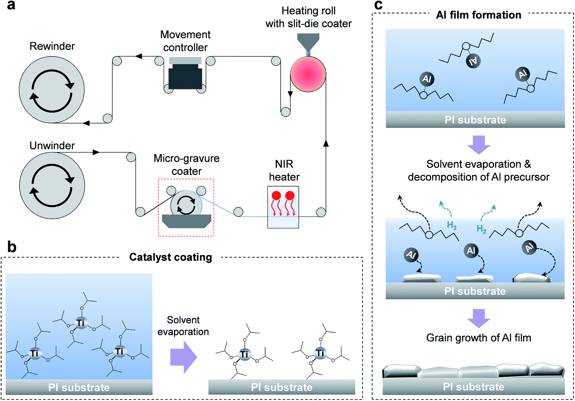 | ||
| Fig. 1 Schematic of the fabricated R2R machine and reaction mechanism. (a) Schematic of the R2R machine. Catalyst coating and Al precursor ink exposure are performed in one step. (b) Catalyst coating mechanism: diluted (100:1) catalyst is coated on the substrate and the solvent is evaporated by heat. (c) Al-film growth mechanism: when the Al precursor ink is exposed to the target substrate (PI substrate), rapid solvent evaporation and decomposition of the Al precursor occur simultaneously. Al film is formed on the PI substrate in seconds. | ||
2.3 Characterization
The surface structure of the Al films was observed using a field emission scanning electron microscope (FE-SEM, Nova230) at 10 kV accelerating voltage. The roughness of the film was measured using an atomic force microscope (AFM, XE-100). To measure the thickness of the Al film, the film was treated by dual beam FIB (Focused Ion Beam) System (Nova 200) and the cross section was observed by SEM. For clear image, Pt film was coated additionally on to the film before treating with FIB. Sheet resistance of the film was measured at least three times by 4-probe system (FPP-HS8), and the average sheet resistance was calculated.2.4 Mechanical endurance tests
A bending test, 3M Scotch tape test, chemical resistance test, and film heating test at 100 °C (Fig. 4c) were performed to investigate the adhesion of the Al film with the substrate and its durability against damage, such as peeling off and heat and chemical resistance. The bending test was performed at a bending radius of 5 mm. In the scotch tape test, a 3M Scotch tape was strongly attached and peeled off from the substrate. Meanwhile, to test the chemical endurance of the film, it was cut and put into a vessel containing either distilled water or ethanol. An air oven (BMD-20, Balman instrument) was used to dry the films at 100 °C in an ambient air atmosphere.2.5 Fabrication of the touch panel
The module of a touch panel was purchased (High Dream LCD) and attached to the touch panel. An indium tin oxide (ITO)-coated PET film was used as the signal collector and placed facing the Al-coated PI film. Copper adhesive tapes were attached to the edge of each signal collectors, passing the signal to the module. To achieve a gap between the two signal collectors and separate the signal pass on each signal collector (ITO film and Al film), a 3M tape (Cat. #3125C) was used as the insulator.3. Results and discussion
3.1 R2R system assembly
We fabricated a unique R2R coating system capable of coating Al thin films on the target substrate using Al precursor ink as the source. Two processes are required to coat the Al film on the target by the decomposition of the Al precursor ink – catalyst coating and ink exposure. The decomposition reaction of the Al precursor ink occurs at over 165 °C in the absence of the catalyst exposure process. However, many impurities, such as Al oxides and AlN, could be formed during the decomposition reaction, which reduce the quality of the Al film. Moreover, when the Al precursor ink is exposed to a high-temperature atmosphere, it decomposes spontaneously due to the low Gibbs free energy of the decomposition reaction.13 Typically, the most effective method to carry out the decomposition reaction of Al precursor ink to a clean Al film without giving rise to any impurities is to apply thermal energy on the target after catalyst exposure. An optimized R2R machine was built considering the best design for Al film coating on the flexible film.3.2 Catalyst exposure and ink coating method
Titanium isopropoxide is a typical catalyst used in the decomposition of Al precursor inks. To enhance the speed of the reaction, very little amount of the catalyst is required. By proper catalyst exposure, high-quality Al films without impurities can be easily coated on the target substrates at certain temperatures (150 °C), while avoiding any damage to the target polymer film.To develop a coating method for the uniform deposition of catalytic solutions, we investigated the coating quality of the catalyzed film obtained from the slit-die coating and spraying methods. Each catalyzed film was dried on a hot plate at 100 °C. The prepared films were analyzed by optical microscopy (Fig. S1 in the ESI†). The slit-die coating method could guarantee uniform deposition of the catalyst, as shown in Fig. S1b,† but it also resulted in a relatively complex structure for maintenance; further, the high price of the device itself poses a disadvantage. On the other hand, the spraying method had the advantages of a simple structure and maintenance, but is inhibited by the high consumption rate of the catalyst. Further, ring-shaped patterns of the sprayed catalyst (about 50 μm in diameter) were formed by the coffee-stain effect on the target substrate. Consequently, the stains of catalyst droplets resulted in a poor quality of the final Al film. The catalyst deposition device should be able to coat extremely thin and uniform catalyst films on the target. Therefore, we chose the micro-gravure coating method due to its simple structure, easy maintenance, competitive pricing, and ability to coat uniform catalyst films on the target as compared to the slit-die and spray coating methods (Fig. S1d†).
Fig. 1b shows a schematic of the catalyst coating process. The uniformly coated catalyst film should be dried fully before exposure to the Al precursor ink because any remaining liquid might reduce the uniformity of the Al film.
The scheme in Fig. 2a depicts the coating of an Al film on the target in a short time period. An Al film is formed rapidly when the Al precursor ink is spread on the catalyst-treated substrate at a certain temperature. During the development of the Al film, the solvent begins to evaporate and hydrogen gas is formed and the target film is completely dried by the end of the reaction. To develop a uniform Al film with low roughness, exact amount of the injected Al precursor ink and the uniform temperature across the target film is required. The decomposition reaction of the Al precursor ink is shown in the following equation:
| 2AlH3O(C4H9)2 → 2Al + 3H2↑ + 2O(C4H9)2↑ | (2) |
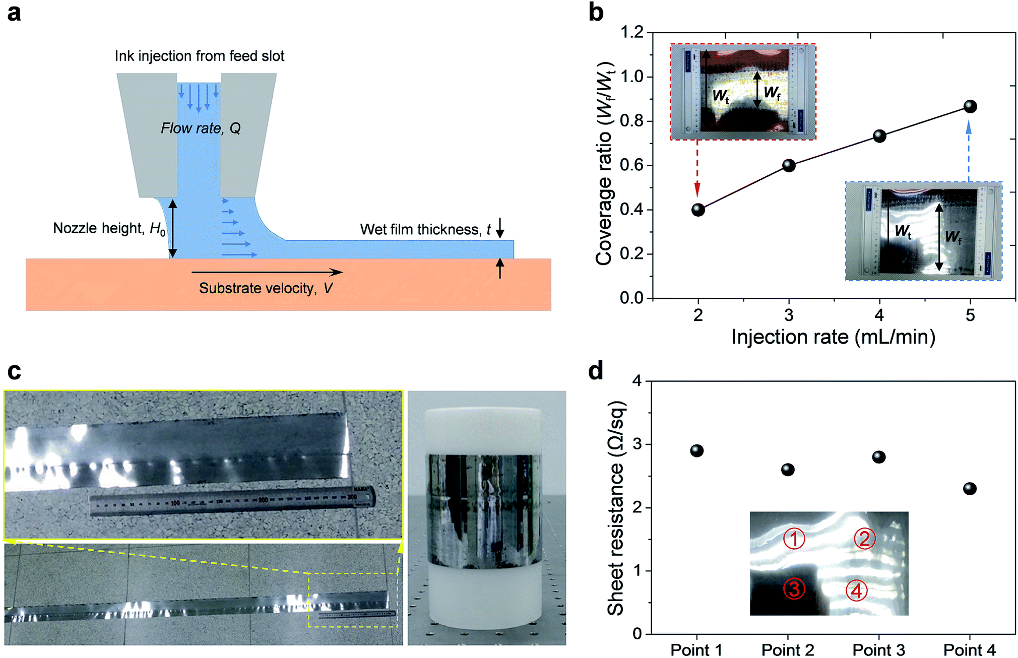 | ||
| Fig. 2 Preparation of Al films by the slit-die coating method on PI substrates. (a) Schematic of the coating bead of the slit-die coater, (b) coverage ratio of the Al film controlled by the injection rate (inset is the film fabricated at an injection rate of 2 mL min−1 and 5 mL min−1), (c) prepared Al film on the PI substrate; the edge of the substrate not completely covered by the Al film was removed, and (d) sheet resistance of the prepared Al film at random points; the inset indicates the points of measurement on the Al film. | ||
The Al precursor is decomposed into Al, hydrogen, and solvent after the reaction. These reactions are basically endothermic. Reaction temperature and catalyst are the two factors that can be controlled to control the speed of the decomposition reaction. As the decomposition of the Al precursor ink is an endothermic reaction, the heat source should be capable of maintaining the temperature at 100–150 °C to ensure constant decomposition. It was difficult to supply enough Al precursor ink to develop the film using the micro-gravure coating method. Therefore, the slit-die coating method was selected to control the exact amount of ink is necessary. A heating roll was used as the heat source for the chemical reaction of the Al precursor. Using this method, it is easy to control the temperature when compared to indirect heating methods, such as IR-lamp heating and hot-air heating. Moreover, sufficient heat could be supplied to the precursor ink simultaneously, which is necessary for the instantaneous reaction of the Al precursor ink with the Al conductive film. The optimized temperature of the heating roll was 150 °C. Stable Al films cannot be obtained continuously at temperatures lower than this value, while higher temperatures damaged the target polymer substrates.
3.3 Low-flow limit evaluation
Before the actual operation of the R2R device, we evaluated its low-flow limit. When the flow is stable, the low-flow limit leads to minimum film thickness at a given fixed web speed. The low-flow limit can be described by the viscocapillary model:22
 | (3) |
The nozzle height should be lower than the evaluated maximum height in order to avoid dewetting of the thin wet film when the ink bead from the nozzle disrupts into randomly scattered droplets. However, narrowing down H0 below a certain limit can cause a nozzle-clogging problem. Because the decomposition of the Al precursor ink into an Al thin film is an endothermic reaction, external thermal energy should be supplied. If H0 is narrow, excess heat can be directly transferred to the nozzle; under such conditions, the Al precursor ink reacts inside the nozzle and blocks it partially or completely. A relatively large H0 over 1.0 mm and continuous flow of the Al precursor ink could prevent nozzle clogging. Therefore, regulating H0 near its limit at the given V is important to obtain stable and high-quality Al conductive films.
3.4 Control over the Al film coverage ratio
To verify the effect of manipulating the injection rate of the Al precursor ink, the injection flow rate was adjusted within a range of 2–5 mL min−1. The coverage ratio was expected to be proportional to the adjustment of the injection rate according to the following relationship:| Q = V × Wf × t | (4) |
As a result, the coverage ratio increased gradually as expected; Fig. 2b shows the coverage ratio curve as a function of the injection rate of the Al precursor ink. The coverage ratio is defined as Wf/Wt, where Wf is the width of the fabricated thin film and Wt is the total width of the PI film. We calculated the thickness, t, of the prepared Al films using the coverage ratio test results. The values of t increased slightly from 11.1 μm to 12.8 μm when Q increased from 2 to 5 mL min−1. In stark contrast, the coverage ratio increased significantly from 0.4 to 0.87. These results indicate the strong dependence of Wf on Q, but not on t, as expected from eqn (4).
Therefore, there was no significant difference in the sheet resistance of the films prepared at various injection flow rates, as shown in Fig. S3†. When the injection rate was lower than 2 mL min−1, ink bead was broken and non-uniform films were obtained. In addition, when the injection rate was higher than 5 mL min−1, the precursor ink flooded over the substrate and random bumps were formed, causing interruptions in the film uniformity. Therefore, it can be concluded that an injection rate of 5 mL min−1 yielded superior film quality in terms of uniformity and coverage ratio.
The R2R device was operated under the optimized conditions and Movie S1† demonstrates the actual operation of the R2R printing system. As shown in Movie S1,† it was possible to fabricate large-scale Al films with high electrical conductivity and mechanical robustness using a one-step process in a very short period of time. The fabricated Al-coated film was wrapped on a plastic roll, as shown in Fig. 2c. From the width of the Al-coated area (0.13 m), it could be calculated that 0.39 m2 of the Al-coated PI film could be fabricated in one minute.
Fig. 2d exhibits the variation in the sheet resistance of the prepared Al film (2.6–2.9 Ω sq−1), which was measured at multiple points, as depicted in the inset of Fig. 2d. There was no significant difference in the sheet resistance, indicating high film uniformity. The Al films prepared at different injection rates of the Al precursor ink showed similar electrical conductivity, as shown in Fig. S3†. This result suggests that the electrical properties of the Al film are not affected by the injection rate, as the film thickness is greatly dependent on the web speed. To modify the electrical conductivity of the films, adjusting the concentration of the Al precursor might be necessary.
3.5 Mechanical properties of the Al-coated PI films
The surface morphology of the R2R-processed Al films was observed by SEM. As shown in Fig. 3a, the R2R-processed Al film consisted of dense grains (∼50 nm in size). The R2R-processed Al film shows a flat surface structure, which is similar to that of an Al-sputtered film (Fig. 3b). Surface roughness of thin films is an important factor in fabricating actual electrical devices. If the surface roughness is too high, considerable short current could be caused at protruding parts of the surface, which eventually leads to device malfunction.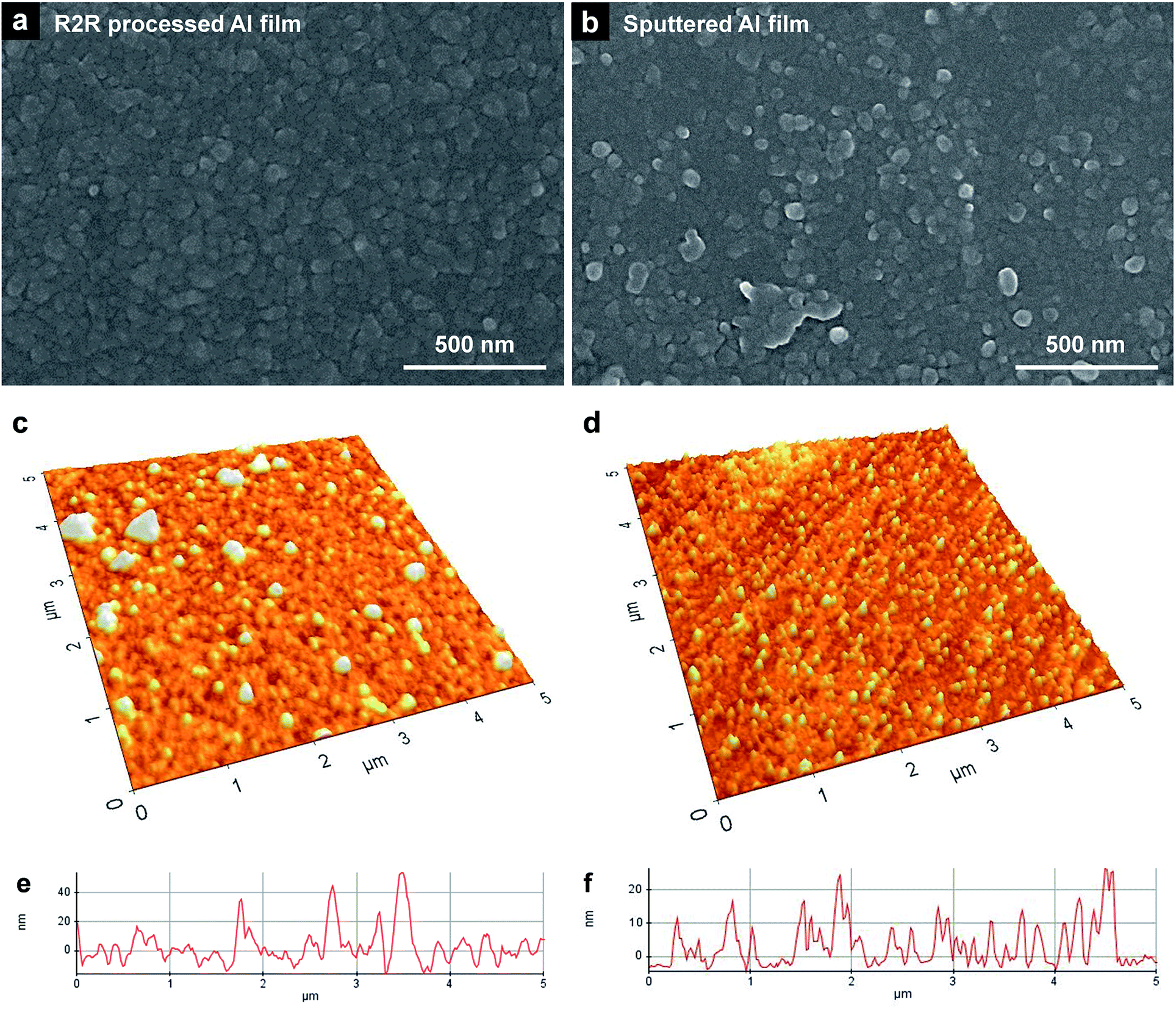 | ||
| Fig. 3 Surface morphology of the Al films prepared using Al precursor ink and sputtered Al film. (a) SEM image of the Al film prepared using Al precursor ink, (b) SEM image of the sputtered Al film, (c) AFM image of the Al film prepared using Al precursor ink. Rrms was measured as 12.4 nm, and (d) AFM image of the sputtered Al film. Rrms was measured as 6.4 nm. (e) and (f) show the line profiles of (c) and (d), respectively. | ||
Surface uniformity and thickness of the film were confirmed by AFM, as shown in Fig. 3c and d. Bumps are formed randomly on the surface of the R2R-processed Al film compared to the Al-sputtered films. The measured Rrms of the R2R-processed Al film was ∼2 times higher than that of the sputtered film; Rrms of the film prepared using the Al precursor ink was 12.4 nm, whereas the Rrms of the sputtered film was 6.4 nm. The measured peak-to-valley value (Rpv) of the R2R-processed Al film was ∼2 times higher than that of the sputtered film. The Rpv of the R2R-processed Al film was 70.1 nm, whereas the Rpv of the sputtered film was 30.7 nm. Even though the surface roughness of the R2R-processed Al film was somewhat larger than that of the Al-sputtered film, it can be applied for the electrodes in electronic devices at the given level of its Rrms.
A mechanical endurance test was performed to evaluate the fabricated Al film on the PI substrate. To apply the Al films for flexible electronic devices, they should exhibit good mechanical stability and electrical conductivity even under harsh conditions. Fig. S4† shows the results of a taping test performed using a 3M Scotch tape to investigate the adhesion durability of the Al film. Even after a successive peeling-off and sticking process, the Al film is attached to the PI substrate very strongly without delamination, indicating good adhesion with the target substrate. Moreover, the electrical resistance of the film was nearly unchanged.
We carried out a bending cyclic test at a bending radius of 5 mm in order to investigate electromechanical stability of the Al film. As shown in Fig. 4a, the value of the normalized resistance, R/R0, remained almost constant, with ∼5% increase in the resistance after 1000 bending cycles. Here, R0 is the initial resistance. The result presents that the Al film has a good mechanical flexibility in conjunction with a stable electrical property even under repeated deformation.
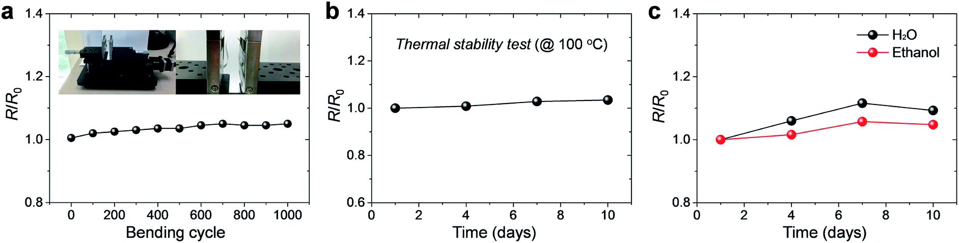 | ||
| Fig. 4 Mechanical endurance of the prepared Al film and its application in electronic circuits. (a) Bending test at 5 mm radius (inset shows the Al film attached to the bending test equipment), (b) heat resistance test at 100 °C, and (c) chemical resistance of the Al film in H2O and ethyl alcohol. | ||
The thermal stability of the films was also analyzed. Typically, in the case of the bulk Al, presence of a dense Al oxide film covering the surface minimalizes further oxidation at 100 °C in ambient air. However, in this case, the Al film coated on the PI film is extremely thin (<100 nm) that the effect of the Al oxide film cannot be assured. The film was kept at 100 °C under ambient conditions for 10 days. Because most of the polymer substrates used in flexible electronics show severe deformation at high temperature of >100 °C, we used 100 °C as a test temperature. The results show that the electrical properties of the films did not experience much change; the resistance of the film increased by only 3% even after 10 days, as shown in Fig. 4b. This suggests that the Al thin film is stable enough under harsh thermal conditions. Further, to confirm the oxidation stability of the films, the Al films were dipped into distilled water and ethyl alcohol baths for 10 days at room temperature (Fig. 4c). At the end of the testing period, the changes in electrical conductivity were quite small (9% and 5% for water and ethyl alcohol, respectively), indicating the high oxidation stability of the Al thin film.
3.6 Flexible touch panel demonstration
To demonstrate the applicability of the R2R-processed Al film in electronic devices, we fabricated a flexible touch panel. The size of the fabricated touch pad was 7 cm × 9 cm. Due to the incorporation of flexible components, the fabricated touch pad also shows high flexibility, as shown in Fig. 5a. An ITO-coated PET film was used as a transparent electrode on one side of the panel and the fabricated Al thin film was used as the counterpart electrode, as shown in Fig. 5b. Copper adhesive tapes were attached to each signal collector as the signal pass to the module. The fabricated touch panel was attached to a laptop using a commercial touch panel optimization software. Fig. 5c shows the operation test of the touch panel and proves that the touch pad works properly; the panel was sensitive enough to write recognizable letters.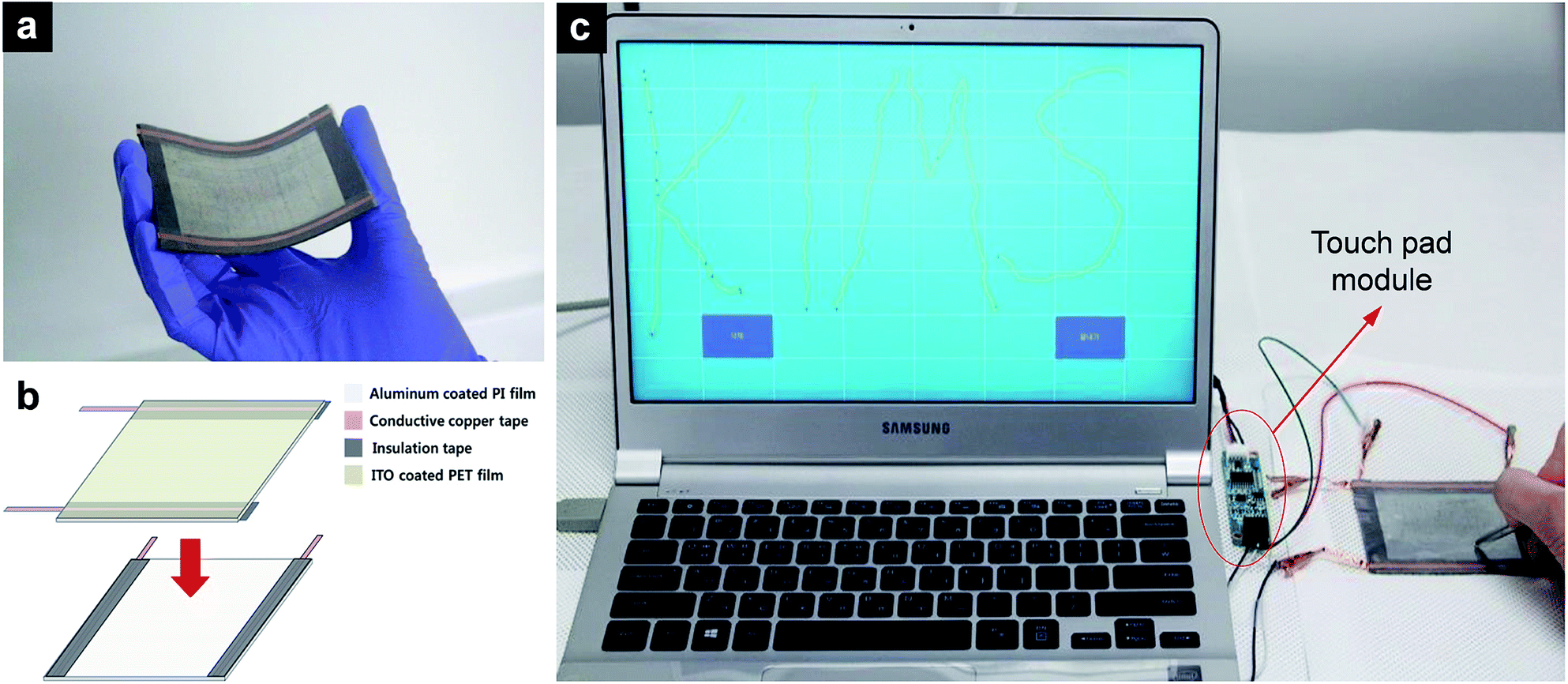 | ||
| Fig. 5 Fabricated touch panel consists of an Al-coated PI film and ITO-coated PET film. (a) Flexibility demonstration of the touch panel, (b) schematic of the fabricated touch panel, and (c) touch screen device connected to a laptop by the module; the flexible touch screen is capable of writing recognizable letters. | ||
4. Conclusions
In conclusion, we developed a one-step R2R process for the large-scale fabrication of Al thin films with high electrical conductivity. To fabricate Al thin films on the substrate, a two-step process was required; these processes included catalyst exposure and Al precursor ink exposure. These two steps were combined into one by using the unique concept of R2R processing for Al coating. After evaluating the low-flow limit at a fixed web speed, the appropriate height of the slit-die was calculated in order to avoid nozzle clogging and dewetting of the wet ink film. Based on the calculations, uniform Al conductive films were fabricated. By adjusting the injection rate of the Al precursor ink, the coverage ratio of the Al film on the substrate could be controlled. At the maximum coverage ratio, 0.39 m2 of the Al-coated film was fabricated per minute on the target flexible polymer substrate. The fabricated film showed high electrical conductivity (∼3 Ω sq−1), low roughness (Rrms 12.4 nm), and showed good mechanical robustness and oxidation resistance under harsh conditions. Using the flexible Al film, a touch panel was successfully demonstrated. This shows the Al-coated PI film can be applied in various electronic devices without the need for complicated processing.Conflicts of interest
There are no conflicts to declare.Acknowledgements
This study was supported financially by the Fundamental Research Program (PNK4661) of the Korea Institute of Materials Science (KIMS).Notes and references
- A. Kamyshny and S. Magdassi, Conductive nanomaterials for printed electronics, Small, 2014, 10(17), 3515–3535 CrossRef PubMed.
- Y. Zheng, Z. He, Y. Gao and J. Liu, Direct desktop printed-circuits-on-paper flexible electronics, Sci. Rep., 2013, 3, 1786 CrossRef.
- Y.-I. Lee, S. Kim, S.-B. Jung, N. V. Myung and Y.-H. Choa, Enhanced electrical and mechanical properties of silver nanoplatelet-based conductive features direct printed on a flexible substrate, ACS Appl. Mater. Interfaces, 2013, 5(13), 5908–5913 Search PubMed.
- K. Ankireddy, S. Vunnam, J. Kellar and W. Cross, Highly conductive short chain carboxylic acid encapsulated silver nanoparticle based inks for direct write technology applications, J. Mater. Chem. C, 2013, 1(3), 572–579 RSC.
- M. Vaseem, K. M. Lee, A.-R. Hong and Y.-B. Hahn, Inkjet printed fractal-connected electrodes with silver nanoparticle ink, ACS Appl. Mater. Interfaces, 2012, 4(6), 3300–3307 Search PubMed.
- T. Yamada, K. Fukuhara, K. Matsuoka, H. Minemawari, J. y. Tsutsumi, N. Fukuda, K. Aoshima, S. Arai, Y. Makita and H. Kubo, Nanoparticle chemisorption printing technique for conductive silver patterning with submicron resolution, Nat. Commun., 2016, 7, 11402 CrossRef PubMed.
- S. Hong, J. Yeo, G. Kim, D. Kim, H. Lee, J. Kwon, H. Lee, P. Lee and S. H. Ko, Nonvacuum, maskless fabrication of a flexible metal grid transparent conductor by low-temperature selective laser sintering of nanoparticle ink, ACS Nano, 2013, 7(6), 5024–5031 CrossRef PubMed.
- M. Berggren, D. Nilsson and N. D. Robinson, Organic materials for printed electronics, Nat. Mater., 2007, 6(1), 3–5 CrossRef PubMed.
- B. Y. Ahn, E. B. Duoss, M. J. Motala, X. Guo, S.-I. Park, Y. Xiong, J. Yoon, R. G. Nuzzo, J. A. Rogers and J. A. Lewis, Omnidirectional printing of flexible, stretchable, and spanning silver microelectrodes, Science, 2009, 323(5921), 1590–1593 CrossRef PubMed.
- Y. Wu, Y. Li, B. S. Ong, P. Liu, S. Gardner and B. Chiang, High-performance organic thin-film transistors with solution-printed gold contacts, Adv. Mater., 2005, 17(2), 184–187 CrossRef.
- A. C. Siegel, S. T. Phillips, M. D. Dickey, N. Lu, Z. Suo and G. M. Whitesides, Foldable printed circuit boards on paper substrates, Adv. Funct. Mater., 2010, 20(1), 28–35 CrossRef.
- Y. S. Rim, S. H. Bae, H. J. Chen, N. De Marco and Y. Yang, Recent Progress in Materials and Devices toward Printable and Flexible Sensors, Adv. Mater., 2016, 28(22), 4415–4440 CrossRef PubMed.
- H. M. Lee, S. Y. Choi, K. T. Kim, J. Y. Yun, D. S. Jung, S. B. Park and J. Park, A novel solution-stamping process for preparation of a highly conductive aluminum thin film, Adv. Mater., 2011, 23(46), 5524–5528 CrossRef PubMed.
- H. M. Lee, S. Y. Choi, A. Jung and S. H. Ko, Highly conductive aluminum textile and paper for flexible and wearable electronics, Angew. Chem., 2013, 125(30), 7872–7877 CrossRef.
- H. M. Lee, H. B. Lee, D. S. Jung, J.-Y. Yun, S. H. Ko and S. B. Park, Solution processed aluminum paper for flexible electronics, Langmuir, 2012, 28(36), 13127–13135 CrossRef PubMed.
- H. M. Lee, J. Y. Seo, A. Jung, S.-Y. Choi, S. H. Ko, J. Jo, S. B. Park and D. Park, Long-term sustainable aluminum precursor solution for highly conductive thin films on rigid and flexible substrates, ACS Appl. Mater. Interfaces, 2014, 6(17), 15480–15487 Search PubMed.
- E. Czech and T. Troczynski, Hydrogen generation through massive corrosion of deformed aluminum in water, Int. J. Hydrogen Energy, 2010, 35(3), 1029–1037 CrossRef.
- E. L. Dreizin, Metal-based reactive nanomaterials, Prog. Energy Combust. Sci., 2009, 35(2), 141–167 CrossRef.
- M. Hösel and F. C. Krebs, Large-scale roll-to-roll photonic sintering of flexo printed silver nanoparticle electrodes, J. Mater. Chem., 2012, 22(31), 15683–15688 RSC.
- F. C. Krebs and K. Norrman, Using Light-Induced Thermocleavage in a Roll-to-Roll Process for Polymer Solar Cells, ACS Appl. Mater. Interfaces, 2010, 2(3), 877–887 Search PubMed.
- R. R. Søndergaard, M. Hösel and F. C. Krebs, Roll-to-Roll fabrication of large area functional organic materials, J. Polym. Sci., Part B: Polym. Phys., 2013, 51(1), 16–34 CrossRef.
- M. S. Carvalho and H. S. Kheshgi, Low-flow limit in slot coating: theory and experiments, AIChE J., 2000, 46(10), 1907–1917 CrossRef.
- S. Bi, G. Zhao and J. Wu, Surface tension of diethyl ether, diisopropyl ether, and dibutyl ether, J. Chem. Eng. Data, 2009, 55(4), 1523–1526 CrossRef.
- X. Meng, J. Wu and Z. Liu, Viscosity and density measurements of diisopropyl ether and dibutyl ether at different temperatures and pressures, J. Chem. Eng. Data, 2008, 54(9), 2353–2358 CrossRef.
Footnote |
| † Electronic supplementary information (ESI) available. See DOI: 10.1039/c8ra03303j |
| This journal is © The Royal Society of Chemistry 2018 |