
 Open Access Article
 This Open Access Article is licensed under a Creative Commons Attribution-Non Commercial 3.0 Unported Licence
Bottom-electrode induced defects in self-assembled monolayer (SAM)-based tunnel junctions affect only the SAM resistance, not the contact resistance or SAM capacitance†
C. S. Suchand Sangeeth‡
a,
Li Jianga and
Christian A. Nijhuis *abc
*abc
aDepartment of Chemistry, National University of Singapore, 3 Science Drive 3, Singapore 117543, Singapore. E-mail: chmnca@nus.edu.sg; Fax: +65 6779 1691; Tel: +65 6516 2667
bCentre for Advanced 2D Materials and Graphene Research Centre, National University of Singapore, 6 Science Drive 2, Singapore 117546, Singapore
cNUSNNI-Nanocore, National University of Singapore, Singapore 117411, Singapore
First published on 30th May 2018
Abstract
In large area molecular junctions, defects are always present and can be caused by impurities and/or defects in the electrode materials and/or SAMs, but how they affect the electrical characteristics of junctions has rarely been studied. Usually, junctions are characterized by two-terminal current–voltage measurements where only the total current across the junction is measured, but with these methods one cannot distinguish how the individual components of the junctions are altered by the defects. Here we show that the roughness of the bottom-electrode is a crucial factor in determining the electrical properties of self-assembled monolayer (SAM)-based junctions. We used potentiodynamic impedance spectroscopy to reveal which components of the junctions are altered by defective bottom electrodes because this method allows for direct determination of all components that impede charge transport in the equivalent circuit of the junctions. We intentionally introduced defects via the roughness of the bottom electrode and found that these defects lower the SAM resistance but they do not alter the capacitance of the SAM or the contact resistance of the junction. In other words, defective junctions can be seen as “leaky capacitors” resulting in an underestimation of the SAM resistance of two orders of magnitude. These results help to improve the interpretation of data generated by SAM-based junctions and explain in part the observed large spread of reported tunneling rates for the same molecules measured across different platforms.
Introduction
Molecular electronic devices can be divided into two classes: single molecule junctions1–5 and junctions based on a layer of molecules with a thickness of exactly one molecule.6–8 Molecular junctions based on self-assembled monolayers (SAMs) are appealing because they operate in the tunneling regime and therefore have complementary properties with respect to conventional devices,6,9–11 and, unlike single molecule junctions,2–4 they can be fabricated on large scales and have found commercial applications,12 and the SAM structure can be characterized in detail.9,13–15 These SAM-based junctions are usually fabricated by first forming a SAM on a metal bottom-electrode followed by the fabrication of a top-electrode on the SAM in a second step.14,16 Although most studies focus on optimizing the second step of the fabrication process,17–20 we21–23 and Whitesides et al.24 have shown that defects in the junctions induced by the defects in the bottom-electrode greatly affect the electrical properties of SAM-based junctions. For instance, by systematically investigating the electrical properties of SAM-based junctions as a function of the surface roughness of the bottom-electrode, we found that the quality of the tunneling barrier defined by the SAM,22 or the performance of a molecular diode,21 depends strongly on the topography of the bottom electrode (see below). Defect free junctions cannot be made and, to a certain degree, defects will be always present due to unavoidable imperfections caused by defects in the electrode materials, e.g., step-edges, grain boundaries, or impurities, or phase domains in the SAMs.21,22,24–26 We note that usually in single molecule experiments only ideal structures are considered and that the role of “defects” or non-ideal structures in these systems are difficult to determine.27–31 Thus understanding how defects affect the electrical properties of junctions, or cause junctions to fail, is important in the rational design of molecular junctions and interpretation of charge transport data they generate.In previous works, we have only pointed out that defects are important and change the apparent values of β,22 or introduce leakage currents reducing the function of molecular diodes,21 here we report which parts of the junctions are affected by defects revealed by impedance spectroscopy. The central question we wish to address here is: which part(s) of the junction, or more specifically, which circuit element(s), is (are) sensitive to defects inside the junction induced by the defects in the bottom-electrode and how will the presence of defects affect the interpretation of charge transport data obtained from SAM-based junctions? The key finding of this work is that imperfections in the bottom-electrode material only affect the SAM resistance whilst other observables associated with typical tunneling behavior (e.g., exponential decay of the current with molecular length) and good quality of the junctions (e.g., high yields), and other circuit components (the capacitance and contact resistance of the junctions) are not affected by defects. Our results show that defective junctions with bottom-electrodes obtained by commonly used direct deposition methods behave as “leaky capacitors” resulting in an underestimation of the SAM resistance by two orders of magnitude. Therefore, this work will be useful for future quantitative analyses of charge transport rates across platforms which has been notoriously difficult (see for a detailed review ref. 14).
Mostly, the electrical properties of SAM based-tunnel junctions are probed with DC conductance measurements which only determine the total current flowing across a junction as a function of applied bias.32–34 DC experiments alone cannot reveal the role of individual junction components (the two SAM–electrode interfaces and the SAM) and usually have to be combined with systematical studies involving changes of the electrode materials or chemical modifications to the SAMs.4,34–41 We note that here we measured the contact resistance directly, without the need for long extrapolations to n = 0, or fitting the low bias linear part of the J(V) curve. In previous works we have compared our values of the contact resistance, and that obtained by others,33,42 and recently we directly compared the contact resistance of EGaIn junctions and conductive probe atomic force microscopy based junctions.43 Here the major difference is that EGaIn junctions have a 1–2 orders of magnitude higher contact resistance due to the presence of the GaOx layer which has indeed a 1–2 orders of higher resistance than bulk EGaIn33,42–44 Fig. 1 shows a SAM-based junction schematically along with an equivalent circuit that describes such a junction consisting of the contact resistance of the SAM (RC) with both electrodes in series with a parallel combination of the SAM resistance (RSAM) and capacitance (CSAM).33,42 This equivalent circuit has been used to model other SAM-based junctions as well.45 We have shown before that frequency dependent impedance measurements make it possible to determine RC, RSAM, and CSAM, and thus to separate the individual components that contribute to charge transport from one and the other.33,46,47 As depicted in Fig. 1, the top-electrode in our studies was fabricated using the “EGaIn-technique” and consists of a eutectic alloy of Ga and In (EGaIn) coated with a self-limiting layer of predominantly Ga2O3 of 0.7 nm thick.33,48 Here, the top electrode forms an ohmic contact with the SAM and the resistance of the GaOx layer and the SAM//top electrode contact (// is a van der Waals interface) are the main contributor to RC.33,42,48 The junction itself can be modelled as a parallel plate capacitor through which a tunneling current flows.23
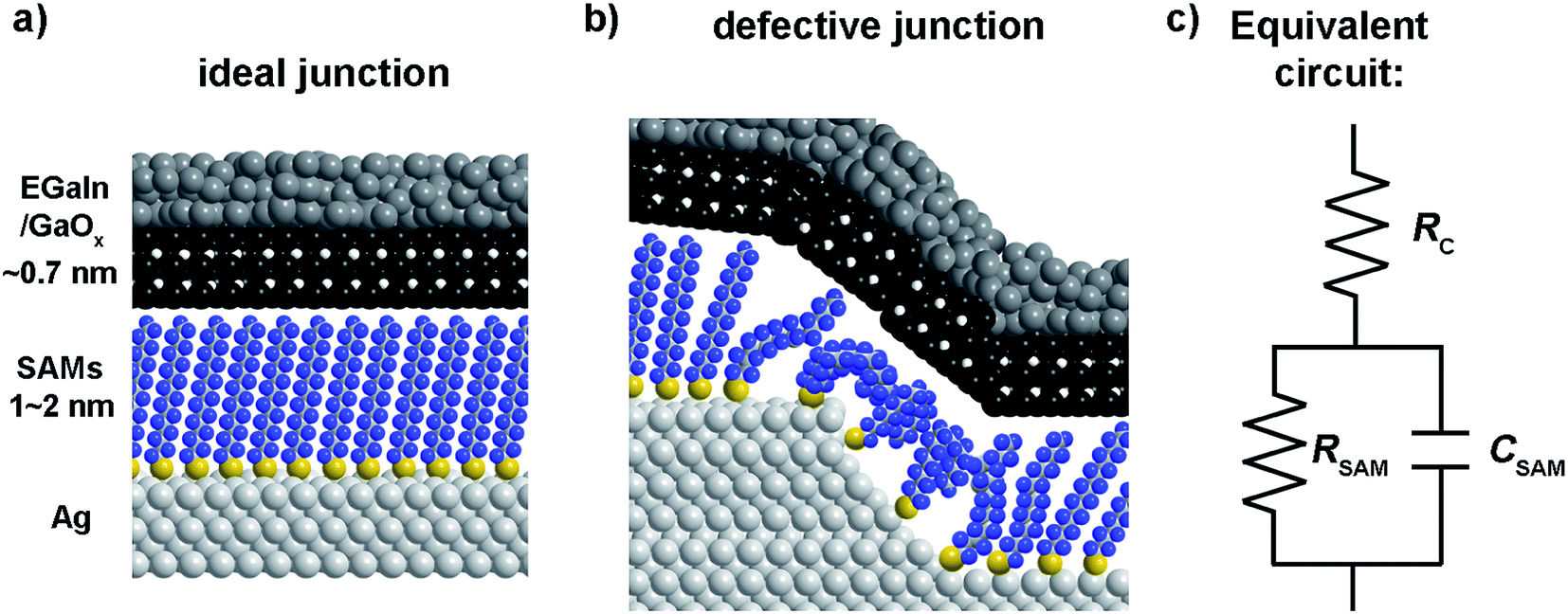 | ||
| Fig. 1 Schematic illustration of an ideal junction without defects (a) and a junction with a disordered SAM on a defect in the bottom-electrode (b). (c) The equivalent circuit of the junction. | ||
The magnitude of the tunneling current density, J (in A cm−2), flowing across junctions with SAMs of, for instance, S(CH2)n−1CH3 (or in short SCn where n is the number of CH2 units) is mostly analyzed with the general tunneling equation (eqn (1))
| J = J0(V)e−βdSAM = J0(V)10−βdSAM/2.303 | (1) |
How defects alter the electrical properties of tunnel junctions have been often characterized in tunnel junctions based on metal oxides,51–54 but not in SAM-based junctions. Based on eqn (1), defective sites in junctions can be classified into two categories: defects that increase (thick area defects) or decrease (thin area defects) the effective electrode–electrode distance.24,55 In EGaIn junctions, large parts within the junction area are thick area defects due to the surface roughness of the EGaIn top electrode;50 these areas do not contribute significantly to the measured value of J as the current flowing across such defect sites are very low. In contrast, the current flowing across thin area defects can be very high and even dominate the measured value of J56–59 and can be caused by, e.g., grain boundaries, chemi- or physisorbed impurities, or phase domains of the SAMs.21,23–26 Here, we used frequency dependent (ranging from 1 Hz to 1 MHz) impedance measurements on tunneling junctions with alkanethiolate SAMs (SCn with n = 10, 14 or 18) formed on Ag substrates with different topographies. By varying the surface topography we effectively varied the root mean square (rms) surface roughness, the grain size, and area of grain boundaries (Agb). To capture all these variables in a single parameter, we used the bearing volume (BV) given by eqn (2) where Ngr is the number of grains.22,60
| BV = Ngr × Agb × rms | (2) |
In terms of BV values, the more defective the bottom-electrodes are, the higher the BV values are. Since we used a top-electrode with an area of 9.6 × 102 μm2 for the electrical measurements of all the junctions, we effectively varied the number of defects inside the tunneling junction by changing BV. We found that defects inside the junctions only affect the SAM resistance, but not the capacitance or the contact resistance of the junction.
Experimental section
Preparation of Ag surfaces
We followed previously reported procedures to prepare the four types of Ag surfaces with different surface topographies.22,60 Generally, we used high grade silver with purity of 99.999% (Super Conductor Material, Inc (USA)) and one-side polished silicon wafers (University Wafers, USA) as the template for templated-stripped (TS) Ag surfaces, or as substrates for Ag surfaces obtained by direct evaporation (DE). The Ag was deposited at a rate of 0.5 Å s−1 for the first 50 nm and followed by the deposition of 250 nm at a rate of 1 Å s−1 (at a base pressure of 2–5 × 10⁻⁶ bar) in the case of AgA-TS, AgTS, and AgDE,1, surfaces. The AgDE,2 surfaces were obtained by deposition of Ag a rate of 4 Å s−1. After deposition of Ag, the AgDE,1 and AgDE,2 substrates were used as such. To obtain the AgA-TS surfaces, after metal deposition the substrates were annealed at 200 °C (the temperature was increased from room temperature at a rate of 15 °C min−1) for 30 min under vacuum inside the vacuum chamber of the thermal evaporate. After annealing, we cooled down the substrates to room temperature overnight inside the UHV chamber. We applied an optical adhesive (OA, Norland, no. 61) on the Ag substrates to glue the glass supports (2 × 3 cm2, cleaned by immersion into piranha solution (H2SO4![[thin space (1/6-em)]](https://www.rsc.org/images/entities/char_2009.gif) :H2O2 = 3:1) for 20 min, followed by washing with H2O and dried in a stream of N2 gas. The size of the glass supports will be the final dimension of the bottom-electrode. Note, we used Ag surfaces in this study since we can generate surfaces with large changes in the BV values as reported previously.21,22,60,61 These glass supports were further cleaned with air plasma for 2 min and then glued to the metal Ag surfaces. We cured the OA/Ag/silicon substrates under UV light (100 watt using a ultraviolet light at a distance of 60 cm from the substrates to minimize heating) for 1 hour. After curing, the glass/AO/Ag stacks were stripped of the template just before use. The AgTS surfaces were obtained in the same way as described above to obtain the AgA-TS but without the annealing step.
:H2O2 = 3:1) for 20 min, followed by washing with H2O and dried in a stream of N2 gas. The size of the glass supports will be the final dimension of the bottom-electrode. Note, we used Ag surfaces in this study since we can generate surfaces with large changes in the BV values as reported previously.21,22,60,61 These glass supports were further cleaned with air plasma for 2 min and then glued to the metal Ag surfaces. We cured the OA/Ag/silicon substrates under UV light (100 watt using a ultraviolet light at a distance of 60 cm from the substrates to minimize heating) for 1 hour. After curing, the glass/AO/Ag stacks were stripped of the template just before use. The AgTS surfaces were obtained in the same way as described above to obtain the AgA-TS but without the annealing step.
Atomic force microscopy
Atomic force microscopy (AFM) images were recorded on a Bruker Dimension FastScan AFM by using tapping mode tips with intermittent contacts (model: FASTSCAN-A, resonant frequency: 14 MHz, and force constant: 18 N m−1).Preparation of the SAMs
We purified the n-alkanethiols (Sigma Aldrich) by recrystallization from ethanol (AR grade; three times) before use because their purity, as received, ranged from 95 to 98%.22,61 Since thiols can decompose and form disulfides in ambient conditions, we further purified the as received n-alkanethiols (Sigma-Aldrich) prior to use. The n-alkanethiols (n = 10, 14 or 18) were recrystallized from ethanol (AR grade) under an atmosphere of N2 at −20 °C followed by a quick filtration. We repeated the recrystallization of each compound for 3 times, and we stored the purified thiols under N2 at 4 °C. We followed a previously reported protocol to prepare the SAMs.22 First, we prepared 3 mM ethanolic solutions of each alkanethiol and purged the solutions with N2 gas for at least 15 min prior to immersion of the Ag substrates. The SAMs were formed over a period of three hours in the ethanolic solutions under inert atmosphere to prevent oxidation of the M–S bond and avoid the formation of silver oxides. The AgDE,1 and AgDE,2 substrates were immersed into the solution immediately after they were removed from the vacuum chamber of the thermal evaporator and the AgA-TS and AgTS substrates were immersed into the solution immediately (within a few seconds) after template-stripping.Fabrication of the junctions
We formed top-contacts on the SAM using GaOx/EGaIn confined in a through-hole in poly(dimethylsiloxane) (PDMS) using a method which has recently been reported by us.61 Here, the liquid-metal is injected in a micro-channel in PDMS; this microchannel was aligned over a through-hole which was connected to a second channel to which vacuum was applied so that the liquid-metal was forced into the though-hole. The slab of PDMS with the GaOx/EGaIn stabilized in the through-hole was gently placed on top of the SAM. After electrical characterization, we removed the top-electrode from the SAM to form a new junction. The same top-electrode could be used to form 20–25 junctions.Electrical characterization of the junctions
The J(V) measurements were carried out using a Keithley 6430 source meter and data were acquired using LabView 2010 following previously reported methods.61 Before we started the impedance measurements, we determined the J(V) characteristics of the devices and recorded the values of J over the range of biases of −0.50 to 0.50 V at intervals of 20 mV. We selected those junctions that had their electrical characteristic within one log-standard deviation from the Gaussian log-mean values of J (which are reported in ref. 22) for the impedance measurements. All impedance measurements were repeated 3 times using 3 different junctions following previously reported procedures reported elsewhere. We measured the impedance of these junctions using a Solartron impedance analyzer (model Solartron 1260A with 1296A dielectric interface) in reference mode with a standard 10 pF capacitor as the external reference (see ref. 33 and 42 for all the details). The potentiodynamic impedance measurements were conducted by applying an AC voltage of 30 mV superimposed on a DC bias voltage and the frequency was varied from 1 Hz to 1 MHz with 10 frequencies per decade. The geometrical junction areas was 9.6 × 102 μm2 in all impedance measurements.Results and discussion
The bottom electrodes
We fabricated four different types of bottom-electrodes with varying surface topographies to investigate how defects induced by the bottom-electrode alters the electrical characteristics, more specifically, the complex impedance of the junctions following previously reported methods (see experimental section for details).22,60 Fig. 2 shows the atomic force microscopy (AFM) images of the four Ag surfaces. These surfaces have different values of the root mean square (rms) surface roughness, number of grains (Ngr), and area of exposed grain boundaries (Agb), Table S1† summarizes these parameters, and we used the bearing volume (BV in nm3; eqn (2)) to compare the topography of these bottom-electrodes. Low BV values indicate the surface is smooth and has low density of defects, while large BV values indicate the surface is dominated by the defects. In agreement with our previous work, AgA-TS and AgTS surfaces have low BV values of 8 × 10⁴ nm3 and 1 × 10⁵, respectively, while that of the AgDE,1 and AgDE,2 surfaces are more than two orders of magnitude larger (∼2 × 10⁶ nm3 and ∼3 × 10⁶ nm3, respectively).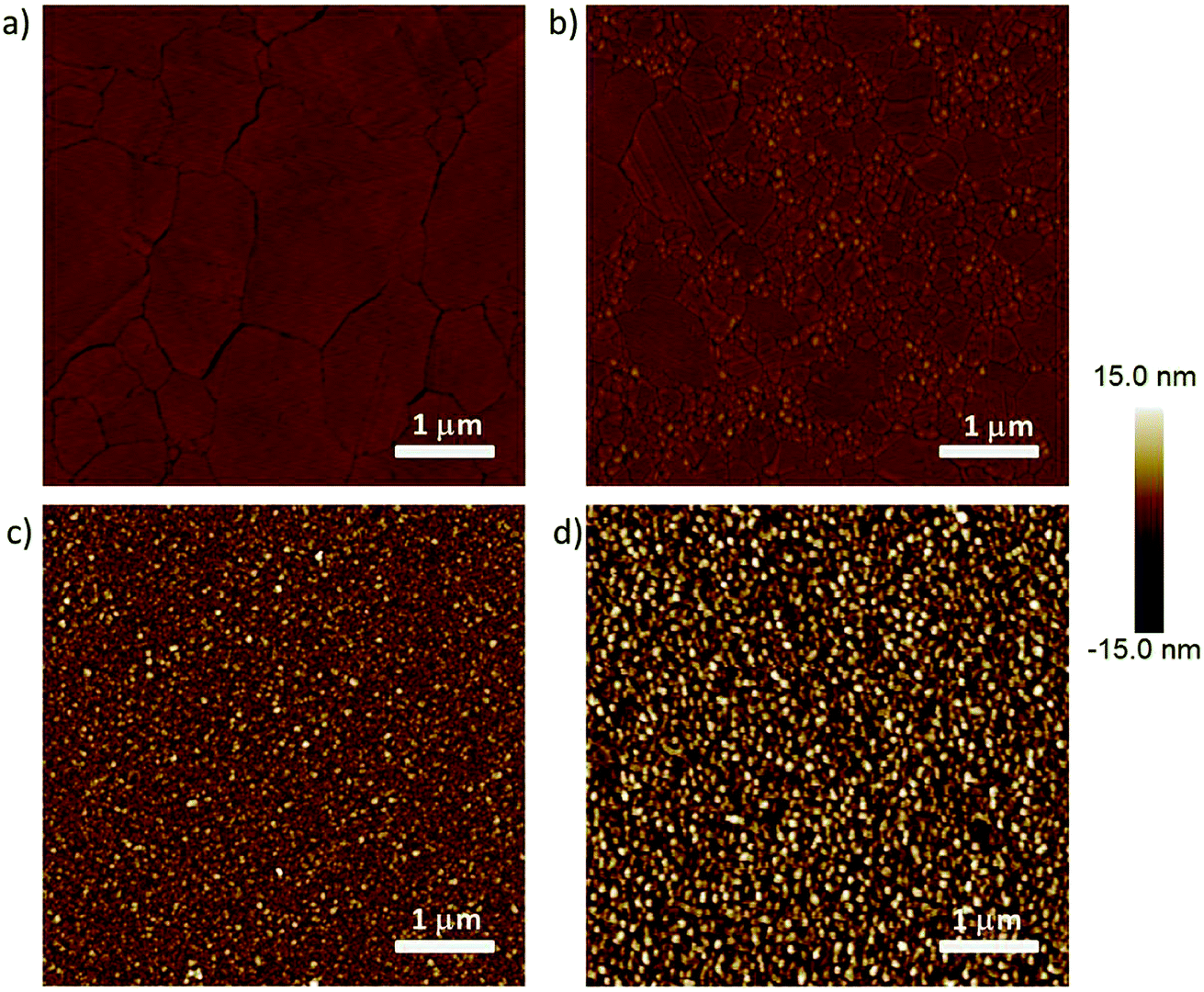 | ||
| Fig. 2 AFM images of the AgA-TS (a), AgTS (b), AgDE,1 (c), and AgDE,2 (d) bottom electrodes. | ||
This large difference in the BV values is also visible by eye in Fig. 2. The AgA-TS surface only consists of large grains separated by wide grain boundaries, while the AgTS surface consists of large grains separated by small grains. Here the effect of annealing is clearly visible as the small grains are effectively removed. In addition, since both types of surfaces were obtained from template-stripping, all the grains are in the same plane defined by the template. In sharp contrast, both types of AgDE surfaces have a large surface roughness because the grains are small and are out of plane with respect to each other. Therefore, the AgDE surfaces have a large surface fraction of exposed grain boundaries at which SAMs cannot pack well while both types of AgTS surfaces have a relatively small amount of exposed grain boundaries.
DC characterization of the junctions
We formed the junctions using a previously reported procedure.61 Briefly, we formed SAMs of n-alkanethiolate SAMs (S(CH2)n−1CH3 ≡ SCn with n = 10, 14, or 18) supported by the four types of silver surfaces. Next, we formed electrical contacts to these SAMs with EGaIn. We used GaOx/EGaIn top-electrodes stabilized in a through-hole in PDMS because these junctions are mechanically stable and suitable to perform the potentiodynamic impedance spectroscopy measurements which took about 2 h per junction to complete.Before we started the impedance measurements, we recorded J(V) curves to confirm the junctions had their electrical characteristics within one log-standard deviation from the Gaussian log-mean J(V) curves reported previously.22 Fig. 3 shows the J(V) curves recorded from the junctions. Here, we repeated our experiments three times and the J(V) curves in Fig. 3 are the arithmetic mean and the error bar represents the standard deviations. From these data, we derived for each type of junction the value of β and J0 by plotting the values of 〈|J|〉 determined at −0.50 V against the number of carbons in the backbone, n, of the SAM followed by fitting the general tunneling equation (eqn (1)) to these graphs. Fig. S1† shows the results and that indeed the current exponentially decays with increasing n. The values of β are 1.03 ± 0.04 and 1.05 ± 0.05 n−1 for junctions with AgA-TS and AgTS bottom electrodes which are close to the consensus value of 1.0 n−1 associated with high quality junctions. In contrast, junctions with AgDE,1 or AgDE,2 bottom electrodes have low β values of 0.54 ± 0.05 and 0.58 ± 0.06 n−1 which is associated with defective junctions and in agreement with our previous findings.22 Despite the different values of β, all junctions with SC10 SAMs have similar values of J. The difference in values of J at 0.5 V as a function of BV, however, is large (two orders of magnitude) for junctions with SAMs of n = 18 as function of the type of surface. These observations have been recently explained by us and we found that junctions with thin liquid-like SAMs (here with n = 10) are capable of self-repair and compensate for defects in the bottom-electrode material, but thick crystalline-like SAMs are not capable of this self-repair and therefore result in defective junctions with large leakage currents flowing at defect sites.25
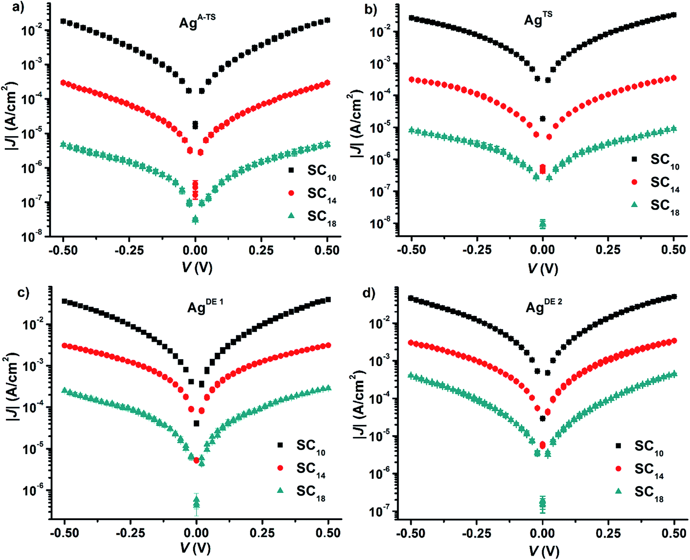 | ||
| Fig. 3 The arithmetic average J(V) characteristics of the junction with SAMs of SC10, SC14, and SC18, supported by AgA-TS (a), AgTS (b), AgDE,1 (c), or AgDE,2 (d), bottom electrodes. The error bars represent the standard deviation obtained from three different junctions. | ||
The equivalent circuit
We have shown before that our junctions can be modelled with a simple equivalent circuit (Fig. 1c) consisting of RSAM in parallel with CSAM both in series with RC.33,42 The complex impedance of this equivalent circuit is given by
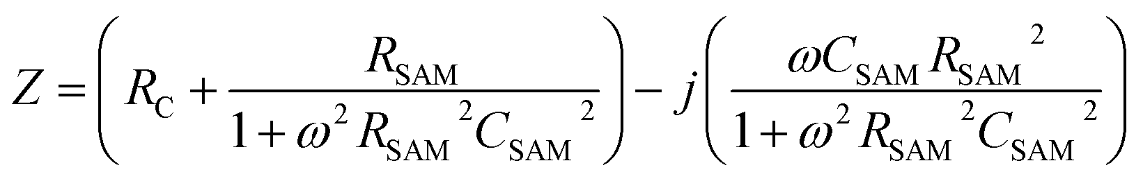 | (3) |
This equivalent circuit implies that SAMs behave as a dielectric placed between two parallel plates (the electrodes). The SAM impedes the current flowing through the junction with a complex impedance which is a parallel combination of RSAM and CSAM. The SAM is coupled to the electrodes through a certain contact resistance RC which is in series with the parallel RC circuit element.
The physical meaning of the equivalent circuit has been discussed before and is summarized here briefly.33,42 In EGaIn based molecular junctions the value of the contact resistance RC is dominated by the SAM//GaOx resistance. In our earlier work we reported that the contact resistances of the contact probes with the electrodes, the Ag–thiolate interface and the low resistance of the GaOx layer only adds about 2% to the measured value RC.42 The resistance of the SAM is given by eqn (4) which relate dSAM to RSAM, where RSAM,0 is the hypothetical resistance across the junction for dSAM = 0 nm.
| RSAM = RSAM,0eβdSAM | (4) |
We interpret the impedance results and equivalent circuit modeling using Landauer tunneling model modified by including the contact resistance term which is associated with the coupling of the molecules to electrodes (eqn (5))62
 | (5) |
| CSAM = ε0εrAgeo/dSAM | (6) |
Potentiodynamic impedance spectroscopy
Impedance (Z) is a more general concept resistance than since it contains both amplitude and phase information of the signal.33 As mentioned in the Introduction, impedance spectroscopy makes it possible to determine all circuit elements of our junctions. Here we determined the impedance spectra as a function of bias, i.e., potentiodynamic impedance spectroscopy, how the defects inside the junctions affect all circuit elements. The impedance measurements were carried out by superimposing a sinusoidal signal (in the frequency range of 1 Hz to 1 MHz) on a DC bias ranging from −0.5 V to 0.5 V at intervals of 0.1 V. To improve the signal-to-noise ratios, we took the average of five impedance measurements at each given bias. This procedure was repeated three times with different junctions and the error bars represent the standard deviation of these three measurements.Fig. 4 shows the frequency dependency of the modulus of the complex impedance (|Z|) for all junctions at −0.5 V (so-called Bode plots). The value |Z| is nearly constant at low frequencies (dominated by the resistance of the SAM), but decreases with increasing frequency as the capacitive reactance Xc decrease with frequency ω (capacitive reactance Xc = 1/ωCSAM). The Nyquist plots (Fig. S3†), the imaginary part of Z (Z′′) plotted against the real part of Z (Z′), show only one semicircle which corresponds to the presence of one capacitor element in the equivalent circuit (the phase is 90° for a capacitor and appears as a semi-circle in the Nyquist plot). At high frequencies, the capacitive reactance becomes negligible and the impedance will saturate to the total contact resistance RC which has a phase of 0° and is independent of the frequency (ohmic behavior). Fig. 4 shows that |Z| of the junctions with SAMs of SC18 decreases over two orders of magnitude when bottom-electrodes with large BV values are used (the AgDE,1 and electrodes AgDE,2) while |Z| does not change significantly as function of BV for junctions with SC10 SAM. These observations agree with the J(V) behavior described above and follow our recent findings that liquid-like SAMs smoothen out the thin area defects easily compared to the long chain crystalline like SAMs.25
 | ||
| Fig. 4 |Z| vs. frequency at 0.50 V obtained from junctions with SAMs of (a) SC10, (b) SC14, and (c) SC18, with different bottom electrodes as indicated. The black solid line is a fit of eqn (3) to the data. The values of RSAM for junction with SC10 (d), SC14 (e), and SC18 (f) vs. VB. Error bars represent the standard deviation obtained from three different junctions. | ||
Before we fitted our data to the equivalent circuit, we determined the quality of the impedance data using the Kramers–Kronig transformation, or simply the so-called KK-test.63 The low χKK2 values (0.9 × 10⁻³ to 1.2 × 10⁻³) indicate that the data are of good quality, no higher harmonics are present, and the junctions were stable during the measurements. Next, we fitted our data to eq. to extract the values of RC, RSAM, and CSAM. The solid black lines in Fig. 4 are fits to eqn (3) (with χfit2 in the range of 1.1 × 10⁻³ to 1.5 × 10⁻³) from which we conclude the equivalent circuit describes our junctions well. In the next section, we describe the circuit elements in more detail.
Fig. 5 shows the variation of RSAM and RC with DC bias voltage as a function of BV for different SAMs. The contact resistance RC is independent of the applied DC bias and BV. These observations indicate that in all cases the contact resistance is ohmic in nature61 and dominated by the van der Waals SAM//top electrode contact which includes the resistance across the GaOx layer. Our previous temperature dependent impedance studies on junctions with alkanethiolate SAMs on smooth electrodes showed that RSAM, RC, and CSAM, do not vary with temperature which indicates that the mechanism of charge transport in this system is to coherent tunneling.42 In the present study, in all cases the value of RSAM decreases exponentially with increasing bias, in agreement with previously reported results.14,33 Therefore, regardless of the number of defects, both defective and good quality junctions show typical tunneling characteristics.
 | ||
| Fig. 5 The SAM resistance (RSAM) and contact resistance (RC) vs. DC bias voltages for junction with SC10 SAMs (a), SC14 SAMs (b), and SC18 SAMs (c). The error bars represent the standard deviation of three independent impedance measurements. | ||
The value of RSAM does not vary significantly as a function of BV for junctions with SC10 SAMs while it varies over two orders of magnitude for SC18 junctions. This observation can be explained as follows. We have suggested before that the thin liquid-like character of SC10 SAMs smoothen out the defects induced by the surface topography of the bottom electrode because the intramolecular van der Waals interactions are weak and so the molecules can relatively easily “fall over” and “fill in” defects. In contrast, thick crystalline-like SC18 SAMs cannot self-repair as efficiently due to the high packing energy of the SAM (due to strong van der Waals interactions between the long alkyl chains).25 Therefore, the latter suffer from thin area defects that reduce the effective thickness of the SAM (dSAM) causing a large leakage current through the junction (see eqn (1)) while the former still forms good tunneling barriers even. Thus, the decrease in RSAM with BV shows that the tunneling junctions formed on rough surfaces are dominated by thin area defects and that thin SAMs can compensate for defects over a wide range of BV values. The contact resistance is not noticeably changed because the area of defects is very small and charge conduction can be dominated even by a single pinhole.64 The presence of the defects in thick junctions is also apparent from the shape of the RSAM vs. V curve which is “flatter” for junctions with SC18 than SC10 SAMs. This change in the shape can be related to conduction through pinholes where the current is concentrated and cause local Joule heating.23
Fig. 6 shows the values of CSAM as a function voltage for all four junctions with different bottom electrode topographies and SAM thicknesses. The value of CSAM shows no significant variation over the investigated DC bias range or value of BV. By fitting a plot of CSAM against 1/dSAM to eqn (6) (Fig. S2†), we found that the value of εr of 3.2 ± 0.3 was the same within error for all junctions, in agreement with previously reported values.33,45,65 Thus, the defects induced by the topography of the bottom electrode did not alter the dielectric constant of the SAMs inside the junctions.
 | ||
| Fig. 6 CSAM vs. DC bias voltage for the junctions with SAMs on by AgA-TS (a), AgTS (b), AgDE,1 (c), or AgDE,2 (d), bottom electrodes. Error bars represent the standard deviation obtained from three different junctions. | ||
Conclusions
Impedance spectroscopy is useful method to characterize how defects affect the junction characteristics
By far most studies of molecular junctions are based on two-terminal electrical measurements using DC methods.16,66,67 Previously, we have shown that the yield in non-shorting junctions and reproducibility of the measurements (i.e., the log-standard deviations of the values of J) are remarkably insensitive to the topography of the bottom-electrode and hence these are poor indicators of the quality of these junctions.23 Therefore it is difficult to determine the quality of the junctions (i.e., whether the junctions are dominated by defects are not) solely based on J(V) characterization.64,68 Recently, we showed that the quality of the junctions can be qualitatively determined by examination the curvature of the dJ/dV curves.23 Here we show that impedance spectroscopy makes it possible to examine the role of defects in molecular junctions and which (circuit) elements are affected. We note, however, that this method only works for large area junctions (junctions with ≫ 1000 molecules) since small area junctions (or single molecule junctions) have too small capacitances (≪ 1 pF) to be measurable reliably.69Defects induced by the electrode roughness results in an underestimation of the resistance of the SAM complicating quantitative analyses of data obtained from different platforms
The potentiodynamic impedance measurements and equivalent circuit modelling show that only the resistance of the SAM (RSAM) is affected due to leakage currents across the SAMs. The contact resistance (RC) and capacitance of the junction (CSAM) are not sensitive to the surface roughness of the bottom-electrode while the value of RSAM changed by two orders of magnitude. In other words, defective junctions behave as if they were leaky capacitors and this observation can explain, at least in part, the large spread of current densities measured for the same type of molecules across different test beds.14 More specifically, often metal electrodes are used to support SAMs that were obtained by direct deposition techniques, and/or the morphology of the electrodes is not reported. Our results, however, indicate that for quantitative analyses and comparisons of charge transport data across different types of junction platforms, it is important to report the morphology of the electrode materials.The dielectric constant is insensitive to defects
The SAM based tunneling junction can be modelled as a parallel plate capacitor with a resistor connected in parallel across which the leakage current through the capacitor flows. For clarity, in this view of the junctions the leakage current across the capacitor is the same as the tunneling current across the SAMs. For a high quality capacitor, the capacitance should be high with a minimal leakage current flowing across it. Here we show that the leakage current through the SAM-based capacitors is sensitive to defects but the dielectric constant is not. This observation explains why the dielectric constant of aliphatic SAMs in other junction platforms based on Hg-drop and PEDOT:PSS electrodes are essentially the same as to the value we report here despite the large difference of the RSAM and electrode materials between these platforms.45,65Grain boundaries are the main cause of leakage currents in EGaIn junctions
The TS surfaces have very low amount of step edges or pinholes.60 The primary source of defects in our junctions with alkanethiolate SAMs originate from the grain boundaries. Therefore, ultra-flat surfaces (rms surface roughness < 1 nm) with large grains help to reduce the density of defects inside the junctions. Vilan et al. achieved grain boundary-free Al films by ultra-fast thermal deposition method.70 These surfaces can support alkylphosphonate monolayers with almost no gauche defects.71 However, in case of the pre-existing defects due to the fabrication procedures (as is the case for commonly used metal electrodes), the choice of the SAM can also help to reduce the effect of the defects induced by the topography of the electrodes due to self-repair.25Conflicts of interest
There are no conflicts to declare.Acknowledgements
We acknowledge the Ministry of Education (MOE) for supporting this research under award No. MOE2015-T2-2-134. Prime Minister's Office, Singapore under its Medium sized centre program is also acknowledged for supporting this research.References
- A. C. Aragones, D. Aravena, F. J. Valverde-Munoz, J. A. Real, F. Sanz, I. Diez-Perez and E. Ruiz, J. Am. Chem. Soc., 2017, 139, 5768–5778 CrossRef PubMed.
- R. Frisenda, R. Gaudenzi, C. Franco, M. Mas-Torrent, C. Rovira, J. Veciana, I. Alcon, S. T. Bromley, E. Burzuri and H. S. J. van der Zant, Nano Lett., 2015, 15, 3109–3114 CrossRef PubMed.
- R. Hayakawa, M. A. Karimi, J. Wolf, T. Huhn, M. S. Zollner, C. Herrmann and E. Scheer, Nano Lett., 2016, 16, 4960–4967 CrossRef PubMed.
- D. Taherinia, C. E. Smith, S. Ghosh, S. O. Odoh, L. Balhorn, L. Gagliardi, C. J. Cramer and C. D. Frisbie, ACS Nano, 2016, 10, 4372–4383 CrossRef PubMed.
- J. O. Island, R. Gaudenzi, J. d. Bruijckere, E. Burzurí, C. Franco, M. Mas-Torrent, C. Rovira, J. Veciana, T. M. Klapwijk, R. Aguado and H. S. J. v. d. Zant, Phys. Rev. Lett., 2017, 118, 117001 CrossRef PubMed.
- M. Baghbanzadeh, C. M. Bowers, D. Rappoport, T. Zaba, M. Gonidec, M. H. Al-Sayah, P. Cyganik, A. Aspuru-Guzik and G. M. Whitesides, Angew. Chem., Int. Ed., 2015, 54, 14743–14747 CrossRef PubMed.
- M. Carlotti, A. Kovalchuk, T. Wachter, X. K. Qiu, M. Zharnikov and R. C. Chiechi, Nat. Commun., 2016, 7, 7 Search PubMed.
- R. M. Metzger, Chem. Rev., 2015, 115, 5056–5115 CrossRef PubMed.
- A. Vilan, D. Aswal and D. Cahen, Chem. Rev., 2017, 117, 4248–4286 CrossRef PubMed.
- G. D. Kong, M. Kim, S. J. Cho and H. J. Yoon, Angew. Chem., Int. Ed., 2016, 55, 10307–10311 CrossRef PubMed.
- H. Jeong, D. Kim, D. Xiang and T. Lee, ACS Nano, 2017, 11, 6511–6548 CrossRef PubMed.
- A. J. Bergren, L. Zeer-Wanklyn, M. Semple, N. Pekas, B. Szeto and R. L. McCreery, J. Phys. Condens. Matter, 2016, 28, 094011 CrossRef PubMed.
- J. C. Love, L. A. Estroff, J. K. Kriebel, R. G. Nuzzo and G. M. Whitesides, Chem. Rev., 2005, 105, 1103 CrossRef PubMed.
- H. B. Akkerman and B. de Boer, J. Phys. Condens. Matter, 2008, 20, 20 CrossRef.
- D. Xiang, X. Wang, C. Jia, T. Lee and X. Guo, Chem. Rev., 2016, 116, 4318–4440 CrossRef PubMed.
- R. L. McCreery and A. J. Bergren, Adv. Mater., 2009, 21, 4303–4322 CrossRef PubMed.
- A. P. Bonifas and R. L. McCreery, Nat. Nanotechnol., 2010, 5, 612–617 CrossRef PubMed.
- H. Haick, O. Niitsoo, J. Ghabboun and D. Cahen, J. Phys. Chem. C, 2007, 111, 2318–2329 Search PubMed.
- D. Q. Gao, F. Scholz, H. G. Nothofer, W. E. Ford, U. Scherf, J. M. Wessels, A. Yasuda and F. von Wrochem, J. Am. Chem. Soc., 2011, 133, 5921–5930 CrossRef PubMed.
- H. B. Akkerman, P. W. M. Blom, D. M. de Leeuw and B. de Boer, Nature, 2006, 441, 69–72 CrossRef PubMed.
- L. Yuan, L. Jiang, D. Thompson and C. A. Nijhuis, J. Am. Chem. Soc., 2014, 136, 6554–6557 CrossRef PubMed.
- L. Yuan, L. Jiang, B. Zhang and C. A. Nijhuis, Angew. Chem., Int. Ed., 2014, 53, 3377–3381 CrossRef PubMed.
- L. Jiang, C. S. S. Sangeeth, A. Wan, A. Vilan and C. A. Nijhuis, J. Phys. Chem. C, 2015, 119, 960–969 Search PubMed.
- E. A. Weiss, R. C. Chiechi, G. K. Kaufman, J. K. Kriebel, Z. F. Li, M. Duati, M. A. Rampi and G. M. Whitesides, J. Am. Chem. Soc., 2007, 129, 4336–4349 CrossRef PubMed.
- L. Jiang, C. S. Sangeeth, L. Yuan, D. Thompson and C. A. Nijhuis, Nano Lett., 2015, 15, 6643–6649 CrossRef PubMed.
- L. Jiang, L. Yuan, L. Cao and C. A. Nijhuis, J. Am. Chem. Soc., 2014, 136, 1982–1991 CrossRef PubMed.
- W. J. Hong, D. Z. Manrique, P. Moreno-Garcia, M. Gulcur, A. Mishchenko, C. J. Lambert, M. R. Bryce and T. Wandlowski, J. Am. Chem. Soc., 2011, 134, 2292–2304 CrossRef PubMed.
- A. Mishchenko, D. Vonlanthen, V. Meded, M. Burkle, C. Li, I. V. Pobelov, A. Bagrets, J. K. Viljas, F. Pauly, F. Evers, M. Mayor and T. Wandlowski, Nano Lett., 2010, 10, 156–163 CrossRef PubMed.
- C. Li, I. Pobelov, T. Wandlowski, A. Bagrets, A. Arnold and F. Evers, J. Am. Chem. Soc., 2008, 130, 318–326 CrossRef PubMed.
- B. Q. Xu and N. J. J. Tao, Science, 2003, 301, 1221–1223 CrossRef PubMed.
- S. V. Aradhya and L. Venkataraman, Nat. Nanotechnol., 2013, 8, 399–410 CrossRef PubMed.
- E. S. Juan Carlos Cuevas, Molecular Electronics: An Introduction to Theory and Experiment, World Scientific, Singapore, 2010 Search PubMed.
- C. S. S. Sangeeth, A. Wan and C. A. Nijhuis, J. Am. Chem. Soc., 2014, 136, 11134–11144 CrossRef PubMed.
- K. C. Liao, L. Y. Hsu, C. M. Bowers, H. Rabitz and G. M. Whitesides, J. Am. Chem. Soc., 2015, 137, 5948–5954 CrossRef PubMed.
- J. Sporrer, J. H. Chen, Z. J. Wang and M. M. Thuo, J. Phys. Chem. Lett., 2015, 6, 4952–4958 CrossRef PubMed.
- Z. T. Xie, I. Baldea, A. T. Demissie, C. E. Smith, Y. F. Wu, G. Haugstad and C. D. Frisbie, J. Am. Chem. Soc., 2017, 139, 5696–5699 CrossRef PubMed.
- C. E. Smith, S. O. Odoh, S. Ghosh, L. Gagliardi, C. J. Cramer and C. D. Frisbie, J. Am. Chem. Soc., 2015, 137, 15732–15741 CrossRef PubMed.
- M. Baghbanzadeh, C. M. Bowers, D. Rappoport, T. Zaba, L. Yuan, K. Kang, K. C. Liao, M. Gonidec, P. Rothemund, P. Cyganik, A. Aspuru-Guzik and G. M. Whitesides, J. Am. Chem. Soc., 2017, 139, 7624–7631 CrossRef PubMed.
- K. S. Wimbush, R. M. Fratila, D. D. Wang, D. C. Qi, C. Liang, L. Yuan, N. Yakovlev, K. P. Loh, D. N. Reinhoudt, A. H. Velders and C. A. Nijhuis, Nanoscale, 2014, 6, 11246–11258 RSC.
- M. M. Thuo, W. F. Reus, F. C. Simeone, C. Kim, M. D. Schulz, H. J. Yoon and G. M. Whitesides, J. Am. Chem. Soc., 2012, 134, 10876–10884 CrossRef PubMed.
- Q. V. Nguyen, P. Martin, D. Frath, M. L. Della Rocca, F. Lafolet, C. Barraud, P. Lafarge, V. Mukundan, D. James, R. L. McCreery and J. C. Lacroix, J. Am. Chem. Soc., 2017, 139, 11913–11922 CrossRef PubMed.
- C. S. S. Sangeeth, A. Wan and C. A. Nijhuis, Nanoscale, 2015, 7, 12061–12067 RSC.
- C. S. S. Sangeeth, A. T. Demissie, L. Yuan, T. Wang, C. D. Frisbie and C. A. Nijhuis, J. Am. Chem. Soc., 2016, 138, 7305–7314 CrossRef PubMed.
- C. A. Nijhuis, W. F. Reus and G. M. Whitesides, J. Am. Chem. Soc., 2009, 131, 17814–17827 CrossRef PubMed.
- H. B. Akkerman, R. C. G. Naber, B. Jongbloed, P. A. van Hal, P. W. M. Blom, D. M. de Leeuw and B. de Boer, Proc. Natl. Acad. Sci. U. S. A., 2007, 104, 11161–11166 CrossRef PubMed.
- A. Wan, C. S. Suchand Sangeeth, L. Wang, L. Yuan, L. Jiang and C. A. Nijhuis, Nanoscale, 2015, 7, 19547–19556 RSC.
- D. Wang, D. Fracasso, A. Nurbawono, H. V. Annadata, C. S. Sangeeth, L. Yuan and C. A. Nijhuis, Adv. Mater., 2015, 27, 6689–6695 CrossRef PubMed.
- W. F. Reus, M. M. Thuo, N. D. Shapiro, C. A. Nijhuis and G. M. Whitesides, ACS Nano, 2012, 6, 4806–4822 CrossRef PubMed.
- J. Chen, Z. Wang, S. Oyola-Reynoso and M. M. Thuo, Langmuir, 2017, 33, 13451–13467 CrossRef PubMed.
- F. C. Simeone, H. J. Yoon, M. M. Thuo, J. R. Barber, B. Smith and G. M. Whitesides, J. Am. Chem. Soc., 2013, 135, 18131–18144 CrossRef PubMed.
- K. P. McKenna and J. Blumberger, Phys. Rev. B: Condens. Matter Mater. Phys., 2012, 86, 245110 CrossRef.
- G. Clark, J. R. Schaibley, J. Ross, T. Taniguchi, K. Watanabe, J. R. Hendrickson, S. Mou, W. Yao and X. D. Xu, Nano Lett., 2016, 16, 3944–3948 CrossRef PubMed.
- U. Chandni, K. Watanabe, T. Taniguchi and J. P. Eisenstein, Nano Lett., 2016, 16, 7982–7987 CrossRef PubMed.
- P. Bampoulis, R. van Bremen, Q. R. Yao, B. Poelsema, H. J. W. Zandvliet and K. Sotthewes, ACS Appl. Mater. Interfaces, 2017, 9, 19278–19286 Search PubMed.
- C. A. Nijhuis, W. F. Reus and G. M. Whitesides, J. Am. Chem. Soc., 2010, 132, 18386–18401 CrossRef PubMed.
- H. Haick, J. Ghabboun and D. Cahen, Appl. Phys. Lett., 2005, 86, 042113 CrossRef.
- C. N. Lau, D. R. Stewart, R. S. Williams and M. Bockrath, Nano Lett., 2004, 4, 569–572 CrossRef.
- T. W. Kim, G. N. Wang, H. Lee and T. Lee, Nanotechnology, 2007, 18, 315204–315211 CrossRef.
- J. M. Beebe and J. G. Kushmerick, Appl. Phys. Lett., 2007, 90, 083117 CrossRef.
- L. Jiang, T. Wang and C. A. Nijhuis, Thin Solid Films, 2015, 593, 26–39 CrossRef.
- A. Wan, L. Jiang, C. S. S. Sangeeth and C. A. Nijhuis, Adv. Funct. Mater., 2014, 24, 4442–4456 CrossRef.
- S. Datta, Electronic transport in mesoscopic systems, Cambridge university press, Cambridge, UK, 1995 Search PubMed.
- J. R. Macdonald and W. B. Johnson, Impedance Spectroscopy Theory, Experiment, and Applications, John Wiley & Sons, Inc., Hoboken, NJ, 2005 Search PubMed.
- D. A. Rabson, B. J. Jonsson-Akerman, A. H. Romero, R. Escudero, C. Leighton, S. Kim and I. K. Schuller, J. Appl. Phys., 2001, 89, 2786–2790 CrossRef.
- M. A. Rampi, O. J. A. Schueller and G. M. Whitesides, Appl. Phys. Lett., 1998, 72, 1781–1783 CrossRef.
- R. E. Holmlin, R. Haag, M. L. Chabinyc, R. F. Ismagilov, A. E. Cohen, A. Terfort, M. A. Rampi and G. M. Whitesides, J. Am. Chem. Soc., 2001, 123, 5075–5085 CrossRef PubMed.
- G. Wang, T. W. Kim and T. Lee, J. Mater. Chem., 2011, 21, 18117–18136 RSC.
- E. B. S. Lundqvist, Tunneling Phenomena in Solids, Plenum, New York, 1969 Search PubMed.
- A. Vilan, D. Aswal and D. Cahen, Chem. Rev., 2017, 117, 4248–4286 CrossRef PubMed.
- I. Levine, A. Yoffe, A. Salomon, W. Li, Y. Feldman and A. Vilan, J. Appl. Phys., 2012, 111, 124320 CrossRef.
- I. Levine, S. M. Weber, Y. Feldman, T. Bendikov, H. Cohen, D. Cahen and A. Vilan, Langmuir, 2012, 28, 404–415 CrossRef PubMed.
Footnotes |
| † Electronic supplementary information (ESI) available: Additional experimental details, Nyquist plots and plots of equivalent circuit parameters as a function BV. See DOI: 10.1039/c8ra01513a |
| ‡ Current address: Department of Physics, National Institute of Technology Calicut, Kerala 673601, India. |
| This journal is © The Royal Society of Chemistry 2018 |