
 Open Access Article
 This Open Access Article is licensed under a Creative Commons Attribution-Non Commercial 3.0 Unported Licence
Infrared microlenses and gratings of chalcogenide: confined self-organization in solution processed thin liquid films†
Priyanka Sachan ,
Radhakant Singh,
Prabhat K. Dwivedi and
Ashutosh Sharma*
,
Radhakant Singh,
Prabhat K. Dwivedi and
Ashutosh Sharma*
Department of Chemical Engineering & Center for Nanosciences, Indian Institute of Technology Kanpur, Kanpur, India-208016. E-mail: ashutos@iitk.ac.in; priyanka.sachan@gmail.com
First published on 6th August 2018
Abstract
This work demonstrates the fabrication of chalcogenide microstructures such as gratings, lenses and needles using a lithographically directed, evaporative self-organization of chalcogenide thin liquid films for the first time. Using a two-step annealing protocol, excess solvent of freshly coated ChG films is eliminated and then the liquid films are patterned using elastomeric masters with continuous or disconnected features during solvent evaporation. Although microcontact printing or capillary flow lithography has been proven to be useful to create continuous gratings and waveguide like structures in solid films, our method overcomes the limitation of structural continuity of the generated pattern and uses self-organization of solute ChG within the master's confinement to produce isolated microstructures. Fabrication of disjointed arrays of microlenses of various dimensions as well as conical shaped needles in ChG thin films has been demonstrated for relevant optical IR applications. This methodology establishes evaporative self-organization of ChG thin films as a viable alternative to creating microstructures in bulk ChG with hot-embossing, bypassing the need for ultra high temperature processing.
Introduction
Chalcogenide materials are of interest for mid infrared optical technologies because of their ideal high refractive index, nonlinear optical behavior, wide transmission window and photorefractive behavior.1,2 However, due to unstable nature of chalcogenides compared to oxides, their use in actual IR devices has been limited so far.3 Out of the entire class of chalcogenide glasses (ChG), selenides have widest transmission range (up to ∼12.5 μm and higher) and their refractive indices are higher than other ChG materials, whereas sulphides are easiest in term of material processing, establishing their distinct advantages in different applications.4 For optical applications such as thermal imaging, various microstructures of ChG such as gratings, lens arrays, waveguides etc. have been explored recently.5–7 Although hot embossing or laser inscribing of these microstructures are well established techniques for bulk ChG in order to demonstrate the feasibility of these methods, patterning of thin films has received more interest recently since typical required heights of these structures is only a few micrometers.7–11 Earlier, these thin ChG films were created with thermal evaporation mostly, but now solution processed ChG films are beginning to show significant advantages on films deposited thermally.1,2,12–22 It has been shown that various amine solvents dissolve ChG via nucleophilic substitution of sulphide or selenide units with amine groups and may prove to be ideal for creating thin films and structures for photonic, electronic or imaging application.12,15,23 Physical, optical and structural properties of solution processed (SP) ChG films have been found to be at par with thermally deposited films if complimented with appropriate annealing.14,15,24,25 Continuous structures such as gratings can be fabricated on SP thin films of ChG using standard lithographic techniques such as microtransfer molding, micromolding in capillaries etc. using the flow properties of liquids.10,26,27 One of the limitations of these methods is requirement of continuous structures in order for liquid to be able to flow into pattern cavities and decorate residual solute on the substrate after evaporation. For a thin film coated on substrate of choice, wetting in confinement is a viable method for creating nano/micro patterns of solute materials using a soft master, irrespective of pattern structures.28–30 In this work, we use SP ChG thin films to create isolated as well as connected patterns using elastomeric stamps as a confining tool. Self-organization of residual solute (ChG in this case) via dewetting leads to formation of smooth patterns within the cavity of original master. The resultant structures can be of the similar or smaller lateral dimensions as the cavity dimensions, which can be controlled by altering the solute concentration. Formation of isolated 3-D structures such as lenses, needles has been demonstrated using a two step annealing procedure (soft bake at low temperature then higher temperature annealing). For demonstrating physical and structural purity of hence created lenses, optical resolution is shown using visible light (which is possible due to residual solvent content in the microlenses before hard annealing). This work establishes confinement dewetting/wetting as a viable technique for patterning ChG thin films for imaging and sensing applications. Advantage of this technique is also enhanced as processing temperature is dropped drastically from previous fabrication works by utilizing solution phase of ChG.31–34 For demonstrating the compatibility and feasibility of this technique with different classes of materials, both selenide and sulphide glass have been tested in this work. Evaporative self-organization of ChG thin solution processed films is a novel and yet simple method of creating desired microstructures used in IR devices.Experimental details
Chalcogenide solutions are prepared by dissolving As2S3 and As2Se3 powder into ethylene-diamine (EDA) and ethanolamine (ETA) solvents. Pieces of As2S3 (IG1, Vitron GmbH, 99.999%) and As2Se3 (IG6, Vitron GmbH, 99.999%) from bulk are finely grounded using clean ceramic mortar and pestle. Solutions of IG1 and IG6 are prepared by mixing grounded glass into ethanolamine (SRL, purity > 99%) and ethylene-diamine (MERCK, purity > 99%) in concentrations between 0.4 g ml−1 to 0.6 g ml−1 (As2Se3 in EDA and As2S3 in ETA). Solution is kept at 60 °C with continuous stirring (Tarson Digital Spinot, at the rate of 900 rpm). The dissolution process completes in 12–18 hours and clear yellow and crimson color solutions are observed for IG1 and IG6 respectively. Viscosity of the prepared solutions increases with the glass loading. The solutions are kept inside a properly sealed and covered glass vial prior to film preparation to minimize solvent contamination and light exposure. Average particle size of these solutions is analyzed using DLS measurements (Backman Coulter, DELSA™ Nano C).For preparing films, solutions are spin coated on glass, germanium or silicon wafers at spin speeds 1000 rpm to 3000 rpm for 15 seconds. Immediately after spin coating, samples are kept on a hot plate at 50 °C for 10 seconds for soft baking as the first step of two stage annealing protocol. Elastomeric stamps of PDMS (containing microchannels, microcups or micropillars; details can be found in ESI†) are brought in conformal contact with now viscous liquid ChG films and then kept on the hot plate again at 40 °C for 4 hours for the second step of baking. Second annealing step removes all the remaining solvent while solute, ChG is reorganized in micro-domains depending on the shape and dimensions of confinement afforded by the master. Characterization of hence prepared thin films and patterned films are done using optical microscope (Carl Zeiss, Axio Observer), FESEM (Zeiss, Supra 40 VP), optical profilometer (aep Technology, Nanomap) and AFM (Agilent Technologies) for imaging. Thickness of films is measured using an ellipsometer (Nanofilm, EP3) and profilometer. For transmission/absorption measurements, FTIR (PerkinElmer, USA) and UV-vis (Varian, Cary 50 Bio) spectrophotometer are utilized. To demonstrate the transparency and feature resolving ability of lens array prepared in this work, a microscope/TEM grid arrangement is used. Visualization of features on TEM grid resolved via ChG microlenses is done with microscope while contact angles of microlenses are measured using live imaging in a goniometer (Krűss, DSA25). All experiments are done with minimum light and moisture exposure to keep ChG free of defects and moisture contaminations resulted from water molecules absorption or photo induced structural changes. Fig. 1 shows a schematic representation of patterning process as well as the set up for testing the template convergence/resolution of TEM grid patterns through microlens array generated via this method.
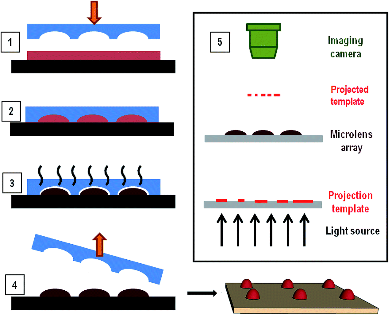 | ||
| Fig. 1 Schematic representation of the ChG pattern formation via liquid film confinement and self-organization: bringing the PDMS mould in contact with viscous liquid ChG film (1 and 2), evaporation of solvent via annealing to render the ChG domains solid (3) and removal of mould after cooling (4). Panel (5) shows the imaging system for testing the converging capability of hence created microlens array. | ||
Results and discussions
ChG materials used in this work are As2Se3 and As2S3, both of which have a wide range of transmission in mid IR spectra of light. For demonstration of our fabrication technique, films of these ChG are coated on different substrates such as glass, quartz, silicon wafer etc. Since this method is independent of substrate properties to a large extent (only the film coating step is affected by surface energy of the substrate), it can be extended to any substrate of choice which is compatible with the solvents chosen in this work.Solution preparation
Dissolution of chalcogenide As2Se3 in EDA takes upto 18 hours while As2S3 in ETA takes upto 10 hours to complete. It is seen that As2S3 has slow but complete dissolution in ETA solvent upto 0.8 g ml−1 concentration. For concentration above 0.6 g ml−1, the kinetics of dissolution needs to be enhanced by heating the solution to 80 °C with agitation. Particle size analysis using a DLS system indicates that average particle size in ChG solution is 160 ± 14 nm after 2 hours of agitation. At the homogenous solution stage after 10 hours of mixing, the solution is highly viscous and opaque hence particle size could not be measured accurately. It is to be noted that the viscosity of ChG–ETA and ChG–EDA solutions increase significantly when stored at room temperature for a few hours. This has been previously observed and explained by chelation of amine bonds that are present in solvent molecules into As2S3 and As2Se3 glass units which increases consistently upon storing. Once the chelation has saturated, the solution reaches equilibrium state and maintains its stability.30 It is also observed that although the dissolution of ChG increases significantly at higher temperatures, the extent of solution contamination due to moisture and oxygen assimilation also increases. Hence the best solution preparation temperature is at 80 °C, with continuous stirring. More detailed solution chemistry is given in ESI.†Film preparation
Solutions of ChG in EDA and ETA are filtered through 0.2 μm syringe filter and dispensed on substrates for spin coating. Films prepared at different rpm are found to have different thickness. The smallest film thickness (0.4% As2Se3 in EDA coated at 3000 rpm, annealed at 50 °C for 2 hour then 80 °C for 2 hours) is ∼900 nm while thickest film (0.6% As2S3 in ETA coated at 1000 rpm, annealed at 50 °C for 2 hour then 80 °C for 2 hours) is of thickness ∼7–8 μm (measured by scratch test with a profilometer). Since the amine solvents have extremely low vapor pressures compared to other commonly used organic solvents for film preparations such as toluene, DMF etc. (VPETA – 0.064 kPa, VPEDA – 1.3 kPa at room temperature), these films contain a large amount of solvent immediately after spin coating. If these films are left at room temperature for solvent evaporation, their surface tension causes the film to retract on substrate surface and thus uneven, rippled and wavy morphology of film (shown in inset of Fig. 3). Thus solvent processed (SP) ChG films have to be annealed appropriately to maintain a smooth and defect free surface. Annealing temperature tested for these films are from 50 °C to 90 °C for 2 hours. It is observed that films annealed at higher temperatures contain more oxygen incorporation induced defects (such as triangular and pyramid shape crystals dotted on the film surface). Triangular crystals of similar kind are reported in a previous study, explained by formation of As2O3 units from As2S3 units in ChG.15 Occurrence of these crystals is reduced by decreasing the annealing temperature, however this results in residual solvent units in film as amine bonds are chelated strongly into amorphous ChG molecules.13,15,18 Fig. 2 shows the morphology of a few ChG films with different annealing conditions to show the defects in high temperature annealed films and relative improvement of surface morphology upon decreasing the annealing temperature. Residual solvents in these films can be eliminated by a short, hard baking step at 90 °C. It has been established that further annealing at 170 °C for a few hours ensures re-polymerization of ChG and thus films with structural properties similar to that of bulk ChG glass can be achieved.13–15,35 It is observed that films annealed at 50 °C for two hours followed by annealing at 80 °C for another two hours result in most defect free films (mean surface roughness ≤ 2 nm) which can later be reinforced structurally by a hard baking step at 170 °C for 2 hours. Two subsequent annealing steps ensure removal of solvent slowly without causing defects at first and then re-bonding of the ChG molecules so that the films regains structural properties similar to bulk glass. | ||
| Fig. 2 FESEM images to show the morphology of films prepared from concentrated solution of ChG (spin coated from 0.6% ETA–As2Se3 solution coated on glass at 2k rpm, ∼4 μm thickness) with different processing conditions. (A), (B) and (C) are films containing defects due to unoptimized film preparation parameters ((A) are crystal defects formed on the surface of films by formation of As2O3 units due to adsorption of oxygen molecules from air, (B) shows a film of large roughness originating from rapid annealing at 140 °C, (C) shows the cracks formed in an otherwise smooth film due to sudden quenching of film temperature from 80 °C to room temperature). (D) showcases a defect free, smooth ChG film, soft baked at 50 °C for 2 hours and hard baked at 80 °C for 2 hours for residual solvent removal (mean surface roughness ≤ 2 nm as shown in the inset AFM profile). All scale bars are 10 μm. | ||
UV-vis and FTIR transmission spectra of these films have been recorded in Fig. 3 to estimate the efficacy of films preparation by this method. Since the substrate of choice is glass, transmission is cut off at ∼3 μm wavelength. UV-vis spectra of a ∼7 μm As2S3 film prepared at three different annealing temperatures are compared for transmission (soft annealing at 60 °C for 2 hours then, 60 °C, 90 °C and 120 °C for 4 hours each). It is observed that cut off of transmission for visible light occurs at ∼450 nm, also indicating high transparency for larger visible wavelengths. FTIR spectrum of these films show some characteristic solvent peaks for C–H and N–H bonds, confirming the requirement of hard baking step of annealing at 170 °C for 2 hours at a later stage.15 Inset of Fig. 3 also shows two images of a smooth defect free As2S3 film (60 °C and 80 °C annealing [1]) as well as a wavy, rippled film (with self assembled undulations formed at room temperature annealing, in [2]). Inset [3] of Fig. 3 is FTIR spectrum of the same film prepared on Ge substrate (which is transparent in the entire mid IR wavelength), showing >50% transmission in the entire IR range. It is to be noted that optical and structural properties of ChG microstructures can further be enhanced by applying suitable annealing post patterning and the protocol can be found elsewhere.12,15,18
 | ||
| Fig. 3 Transmission of ∼7 μm As2S3 films in UV spectrum, showing that transmission of hence prepared films decline with annealing temperature (60 °C, 90 °C and 120 °C for 4 hours each), which can be explained by removal of transparency associated with residual solvent molecules. Cut off of transmission occurs at ∼440 nm, indicating that for red light source, films are somewhat transparent. Insets show a smooth, defect free film [1], a wavy, undulated film [2] and FTIR of film [3]. | ||
Patterning of ChG films within confinements
Following the 2 hours 50 °C soft baking and 80 °C hard baking steps, defect free films are created with thickness of the order of ∼5–9 μm. Tg of As2S3 and As2Se3 are of the order ∼160 °C while the solvent amines evaporate upto processing temperature 120 °C. It is evident during soft annealing step that the solvent (especially ETA, boiling point 170 °C) still persists in ChG films to a large extent for a long time. It has been established that upon evaporation of solvent, non-volatile solute domains self-assemble in a disordered manner over the substrate.36–39 Evaporative self-organization of non-volatile components has been tested as an easy approach to form micro/nano domains in a defined order.30,39 Taking advantage of part solvent present in the freshly coated ChG films, same strategy can be used to confine and organize ChG units in a pre-patterned order. Concentration of solute determines the size and shape of these domains, as the other control parameters such as pattern dimensions, processing temperature, molecular weight of solute, substrate etc. have been kept constant. Confinement to liquid ChG films is provided by using elastomeric PDMS masters. Patterns on these masters can be continuous such as channels, waveguides etc. or isolated such as microlens and pillar arrays. Efficacy of using lithographic confinement for pattern generation is demonstrated in two separate sections for these two types of geometries.Gratings
PDMS moulds containing 40 μm high gratings are used for creating patterns in ChG thin films. Freshly coated films are kept for soft baking at 40 °C for 5 minutes. Majority of residual solvent is removed during this period which can be observed by a slight darkening in film color as well. At this stage, PDMS mould is brought into contact with films containing minimal amount of solvent (and hence a highly concentrated binary system of ChG and solvent). This leads to re-arrangement of concentrated ChG solution within confinement of PDMS channels. Soft annealing at 50 °C is continued for 2 hours followed by hard annealing at 80 °C for an hour. PDMS mould is removed leaving non-volatile ChG in confinements of channels in a smooth, continuous fashion. FESEM images of hence prepared gratings of As2Se3 (channel width 40 μm, length 3 mm and height 35 μm) are shown in Fig. 4, as well as the profile of gratings in [A] that shows an average surface roughness to be less than 2 nm. Reflowing of the hence prepared gratings can be done by standard heating procedure above Tg method (at 220 °C for 4 hours in vacuum). This results into flowing of sharp edges into rounder shape if required. Reflowing of glassy ChG also decreases the surface roughness of these structures further. Dimensions of lateral confinement are flexible and patterns with micro to nano dimensions can be created using appropriate moulds. Depending upon the solute concentration, an under-layer of ChG may be left if mould cavities have been filled and excess solute is left (similar to formation of a residual under-layer in imprint lithography). | ||
| Fig. 4 FESEM images of gratings of As2Se3 (channel width 40 μm, length 3 mm and height 35 μm) before reflow (A), after reflow at 220 °C for 4 hours in vacuum (B). Scale bars are 50 μm. Profile of gratings in (A) and a 3-D rendering is shown in (C). | ||
It is clear while optimizing patterning parameters, that it is crucial to perform the first soft baking step. If excess solvent is trapped within mould, it leads to bubbling during evaporation and hence coarse microstructures are resulted. So the mould is brought into contact with the viscous film at 5 minutes into the 2 hour long soft baking procedure.
Microlenses and isolated microstructures
PDMS moulds containing 400/100 μm diameter depressions of depth 50 μm are used for creating a microlens array in ChG thin films. Freshly coated films are kept for soft baking at 50 °C for 5 minutes, followed by placement of PDMS mould for 2 hours more which is then removed and formed patterns are further annealed at 80 °C for 2 hours. Depending upon the process parameters, quality of microstructures created is altered. A few morphologies of such film structures are reported in Fig. 5. If the ChG film is too thin (thickness of the order of <1 μm), it dewets on the substrate due to the inherent instability of thin film systems, compounded by liquid state of films.40–44 This results into a smooth spherical ChG formation at the centre of the cavity of confining mould Fig. 5(A).45–47 When the film thickness is small compared to the mould height, rim like structures are formed within the cavity, owing to the coffee staining effect Fig. 5(B).39 When the mould height is smaller than the film thickness, an under layer of solute is left. If the mould is removed quickly while the film is in liquid state, some of the solute may adhere to the mould, resulting into fractured top of otherwise smooth structures Fig. 5(C). With insufficient solute concentration, the lateral pinning of edges leads to formation of shallow structures. In Fig. 5(D), a ∼5 μm thickness film when confined within a 50 μm depth cavity forms a microlens of diameter and height ∼18 μm. All of these demonstrate some of the probable outcomes of different process parameters, establishing the need for optimization of effective patterning.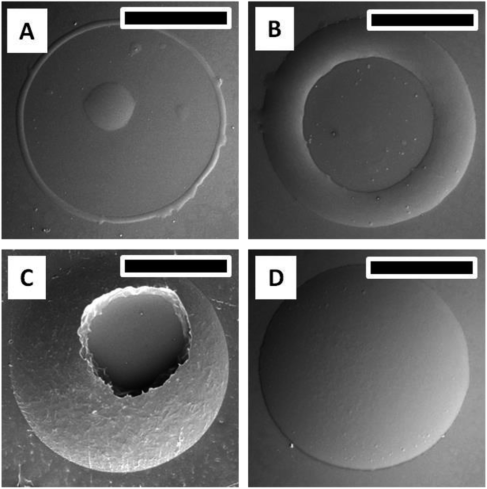 | ||
| Fig. 5 FESEM images of some As2Se3 microlenses generated at different process parameters (mould diameter 100 μm and height 50 μm). Microstructures generated by dewetting within mould confinement (A), rims formed by coffee staining (B), fractured and rough top of microlens upon early mould detachment (C) and shallow microlens with low aspect ratios (D). Scale bars are 50 μm. | ||
Array of microlenses of 400 μm diameter and 50 μm height (SAG) are created using optimized process parameters. Films of thickness ∼11 μm are soft baked for 5 minutes at 50 °C so that only a small fraction of solvent is contained. PDMS moulds of microlens cavities array with above mentioned dimensions are placed on top of viscous liquid ChG films then annealed for 2 hours at 50 °C and 80 °C subsequently. After removal of moulds, patterns are kept at elevated temperature (120 °C) for one hour. Microlens array (of plano-convex lenses) of square lattice arrangement is fabricated on glass substrate. Fig. 6 shows optical image of one such array (A), magnified FESEM image of microlenses (B), a goniometric image showing the contact angle of ∼34° of one such lens (D), and a transverse tilted view of the same lens array in (C) and (E). Surface of these microlenses are exceptionally smooth, due to the self-organized nature of these structures.
 | ||
| Fig. 6 Optical and FESEM images of some As2S3 microlens arrays generated with mould diameter 400 μm and height 50 μm. (A) is a top view of the array imaged with a microscope, (B), (C) and (E) are FESEM images of the same at different magnifications and orientations, showing the smoothness of created lenses and profile at an angle. Scale bar in (E) is 400 μm. (D) is a contact angle goniometer image of one such lens taken from the front, indicating a contact angle of ∼34°. | ||
Profilometry of these arrays is performed and shown in Fig. 7. Top view spanning an area of 1.5 mm × 1.5 mm is scanned. Line profile drawn in the image shows off lateral diameter of ∼300 μm and lens height ∼50 μm. 3-D rendering of this array is shown in the inset. Profilometer image also confirms the finding in Fig. 6 that the individual structure topography is smooth and defect free. Surface roughness of these microlenses is ultralow (≤2 nm), establishing the viability of this fabrication methodology in creating useful optically useful structures.
 | ||
| Fig. 7 Contact profilometer images of As2S3 microlens arrays generated with mould diameter 300 μm and height 50 μm. Top view and 3-D view of this array indicates the smooth surfaces formed with self-organization. Line profile of this array shows the height of created lenses to be ∼50 μm and ∼300 μm lateral diameter, replicating the original mould dimensions. | ||
Geometrical and optical properties of microlens arrays (MLAs) of ChG are compiled in Table 1. For geometrical focal length calculations, lens formulae for plano-convex lens are used.48,49 Experimental calculations are based on distances of different focal planes (of object from lens plane, u and of converged/magnified image from lens plane, v) as measured by a microscope. Lens aperture and dimensions can easily be tailored using the mould dimensions and film thickness.
| Diameter (μm) | Height (μm) | CA (°) | Calculated focal length (μm) | Measured focal length (μm) | Calculated numerical aperture |
|---|---|---|---|---|---|
| 100 ± 2.9 | 50 ± 0.9 | — | 31.3 ± 1.4 | — | 1.6 ± 0.004 |
| 200 ± 5.4 | 50 ± 1.6 | — | 78.1 ± 0.9 | — | 1.28 ± 0.003 |
| 300 ± 4.9 | 50 ± 2.1 | 43 | 156.3 ± 2.3 | 181.3 ± 2.3 | 0.96 ± 0.002 |
| 400 ± 6.4 | 50 ± 1.9 | 34 | 265.6 ± 4.7 | 314.4 ± 3.8 | 0.76 ± 0.003 |
Quality assessment of ChG microlens array with optical imaging
Microlens arrays (MLA) of ChG fabricated using this method are tested for optical applications in visible spectral range. As the application for which these structures are created is in IR range, it would be judicious to characterize them with IR light but due to unavailability of required experimental set-up, an exploratory testing is performed using visible light. Due to the plano-convex geometry of lenses produced, the array exhibits a converging capacity. It has been already established that ChG films and structures thus created have enough transmission in UV region because of the residual solvent (cut off at 450 nm wavelength, shown in Fig. 3), imaging of a target under white light is a possible route to test the converging capacity of these lenses. For IR optical applications, these MLAs can be annealed at temperatures above 180 °C for 2 hours in vacuum for structural reinforcement of ChG units to ensure complete solvent removal and sufficient IR transparency. As optical detector, Leica microscope with 5× and 10× magnification is used. The objects to be imaged are a TEM grid (of 100 μm aperture) and a display LED array. Schematic illustration of optical set up is shown in Fig. 1.50–53 Rows A and B of Fig. 8 are different focal planes imaged with low and high magnification, respectively. Fig. 8(A1) is the LED display to be imaged by MLA, showing green, red and blue light LEDs. When the focus is adjusted to the MLA surface, a 3 × 3 array of ChG microlenses (As2S3 microlenses, diameter ∼300 μm and height ∼50 μm) becomes visible in Fig. 8(A2). When the focus is further shifted to the MLA's focal plane, a projection of LED display in Fig. 8(A1) through the converging MLA in Fig. 8(A2) is seen in Fig. 8(A3). As can be seen, all the individual lenses are projecting and resolving the LED display at the same focal plane, confirming the uniformity and clarity of microlenses generated. Row B shows a single lens of this array resolving and converging a hexagonal TEM grid of opening 100 μm. Fig. 8(B1) is the focal plane where the TEM grid is visible, Fig. 8(B2) is the plane where the ChG lens is kept, then Fig. 8(B3) shows the de-magnified TEM grid as seen through the ChG lens. Scale bars in Fig. 8(A2) and (B2) are 300 μm. In Fig. 8(A1) and (B1), defocus lens impressions are visible at the same locations where the microlenses can be seen after focusing in Fig. 8(A2) and (B2). This establishes the clarity and structural/physical integrity of ChG films and structures prepared in this work. For IR uses, samples need to be hard baked further for complete solvent removal and re-polymerization of ChG.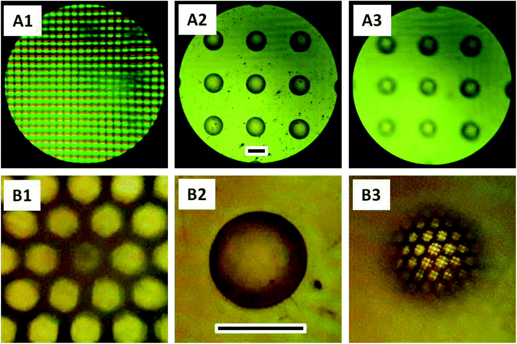 | ||
| Fig. 8 Demonstrating the optical characteristics of a microlens array (MLA) consisting of ∼300 μm diameter and ∼50 μm height lenses. (A1)–(A3) show the three different planes of focus, target object plane, MLA plane and MLA's focal plane. (A3) shows the converged target object in (A1) as focused by the MLA. (B1)–(B3) are the same three planes for a single lens, showing a magnified target (hexagonal TEM grid), microlens and converged image of the TEM grid. | ||
Similar to the microlenses, other discrete, isolated structures can also be created using the self-organization. One such array of needle like structures is also demonstrated using pillar shape confinement. PDMS mould used for creating these geometries contain pillar like holes with 20 μm diameter and ∼40 μm height. When a ∼11 μm ChG film is provided lithographical confinement with this mould, smooth high aspect ratio microstructures, such as microcones array is created. As can be seen by high magnification FESEM image in the inset of Fig. 9, hence created structures are free of surface defects and roughness due to self-organized nature of the process. Thus, it is possible to fabricate smooth 3-D structures of various geometries using evaporative self-assembly and lithographic confinement of ChG films containing residual solvent after soft annealing step.
 | ||
| Fig. 9 FESEM images of 3-D microcones array consisting of ∼20 μm wide microcones. Inset is showing one such microcone magnified to establish the high surface smoothness. Background roughness of underlayer is caused by evaporation of trapped residual solvent while confined under the mould. Scale bar is 50 μm. | ||
One of the additional advantages of using low temperature self-organization is in the form of freedom of choosing a substrate. For film preparation, a uniform, clean substrate is the only requirement. Thus, all conventional substrates that are optically suitable are open for this fabrication process. For proof of concept, we have successfully created microlens arrays of ChG on Borosilicate glass, ChG glass slab, Ge/Si wafers and quartz.
Although this methodology is inspired from both thin film dewetting in confinement as well as hot embossing, there are fundamental differences. In a confined thin film dewetting, film thickness are in nanometer range as instability is primarily observed in films where intermolecular forces are of significance.46,54,55 For these forces to make an impact on the film morphology, film thickness has to be small enough that stabilizing gravitational force fails to keep the film intact. In contrast, as our feature sizes are in micrometer to millimeter range, our film thickness is also in micrometer scale. Hot embossing and nano imprint lithography of a pattern master is done on single phase material by stamping it after softening it beyond its softening temperature.32,56 Our methodology uses two phase films which contain a large amount of solvent hence reducing the process temperature. When hot embossing is performed on pure chalcogenide films/blocks, stamping temperature is >220 °C as ChG is thermally stable.8,10,33 However in a solution phase, when mixed with an organic solvent, the mixed phase ChG films retain their softness and hence self-organization is feasible at even lower temperature. For solvent eliminations, heating is only required to facilitate solvent evaporation (process temperature < 200 °C).
Conclusions
This work demonstrates the lithographic confinement of micron thickness liquid ChG films as a fabrication method to create various continuous or isolated microstructures with minimal surface roughness (≤2 nm) for the first time. Amine solution processed ChG films have residual solvent molecules in glass matrix, hence retaining the liquid nature of the films. In order to create defect free ChG glass films, a two step annealing process has been optimized. Taking advantage of the liquid state of the freshly prepared films, a lithographically confined self-organization is explored for fabricating micro patterns that are optically useful. Performing soft annealing step immediately after coating the film for a few minutes eliminates majority of the solvent, which results into ChG films in viscous liquid state with residual solvent. At this stage, PDMS moulds containing gratings and microlens arrays are brought into conformal contact of these films. Upon hard baking, residual solvent is evaporated, leaving behind solid, smooth micropatterns of ChG which are self-organized within the cavities of PDMS mould. Imaging capability of these microlens arrays are demonstrated using a projection template and focal length of these lenses are calculated via geometrical calculations as well as experimental measurements of object and image distances from lens plane. This work demonstrates applying lithographic confinement to liquid ChG films as a diverse fabrication technique applicable on different ChG materials. We are able to create optical microstructures in thin films, thus simplifying the process requirements from a bulk hot embossing protocol which is the standard in ChG patterning so far. Liquid state self-organization of ChG in a two step process is shown to be a competent, simple, efficient and improved method of forming glassy microstructures on a choice of substrate.Conflicts of interest
There are no conflicts to declare.Acknowledgements
This work is supported by Center for Nanosciences at IIT Kanpur. We would like to thank DRDO for their support for this work via their project ERIP/ER/1200448/M/01/1543.References
- A. Zakery and S. R. Elliott, Optical Properties and Applications of Chalcogenide Glasses: A Review, J. Non-Cryst. Solids, 2003, 330, 1–12 CrossRef.
- A. B. Seddon, Chalcogenide Glasses: A Review of Their Preparation, Properties and Applications, J. Non-Cryst. Solids, 1995, 184, 44–50 CrossRef.
- M. F. Churbanov, V. S. Shiryaev, V. V. Gerasimenko, A. A. Pushkin, I. V. Skripachev, G. E. Snopatin and V. G. Plotnichenko, Stability of the Optical and Mechanical Properties of Chalcogenide Fibers, Inorg. Mater., 2002, 38, 1063–1068 CrossRef.
- J. A. Savage, Infrared Optical Materials and Their Antireflection Coatings, 1985 Search PubMed.
- D. Vandormael, S. Habraken, J. Loicq, C. Lenaerts and D. Mawet, Antireflective Subwavelength Patterning of Ir Optics, Proc. SPIE-Int. Soc. Opt. Eng., 2006, 6395 Search PubMed.
- A. Saitoh, T. Gotoh and K. Tanaka, Chalcogenide-Glass Microlenses for Optical Fibers, J. Non-Cryst. Solids, 2002, 299–302, 983–987 CrossRef.
- M. Popescu, A. Velea, S. Miclos and D. Savastru, Optics of Microlenses Created by Irradiation of as 2s 3 Amorphous Chalcogenide Films with Femtosecond Laser Pulses, Philos. Mag. Lett., 2013, 93, 213–220 CrossRef.
- T. Kohoutek, J. Orava, A. L. Greer and H. Fudouzi, Sub-Micrometer Soft Lithography of a Bulk Chalcogenide Glass, Opt. Express, 2013, 21, 9584–9591 CrossRef PubMed.
- T. Kohoutek, M. A. Hughes, H. Kawashima, M. Mastumoto, T. Misumi, T. Suzuki and Y. Ohishi, In Highly Efficient Relief Diffraction Gratings Inscribed on a Chalcogenide Bulk Glass by a Femtosecond Laser, 2012, p. 2012 Search PubMed.
- C. Tsay, Y. Zha and C. B. Arnold, Solution-Processed Chalcogenide Glass for Integrated Single-Mode Mid-Infrared Waveguides, Opt. Express, 2010, 18, 26744–26753 CrossRef PubMed.
- N. J. Baker, H. W. Lee, I. C. M. Littler, C. M. De Sterke, B. J. Eggleton, D. Y. Choi, S. Madden and B. Luther-Davies, Sampled Bragg Gratings in Chalcogenide (As2S3) Rib-Waveguides, Opt. Express, 2006, 14, 9451–9459 CrossRef PubMed.
- Y. Zha, M. Waldmann and C. B. Arnold, A Review on Solution Processing of Chalcogenide Glasses for Optical Components, Opt. Mater. Express, 2013, 3, 1259–1272 CrossRef.
- Y. Zha, S. Fingerman, S. J. Cantrell and C. B. Arnold, Pore Formation and Removal in Solution-Processed Amorphous Arsenic Sulfide Films, J. Non-Cryst. Solids, 2013, 369, 11–16 CrossRef.
- Y. Zha and C. B. Arnold, Solution-Processing of Thick Chalcogenide-chalcogenide and Metal-Chalcogenide Structures by Spin-Coating and Multilayer Lamination, Opt. Mater. Express, 2013, 3, 309–317 CrossRef.
- Y. Zou, H. Lin, O. Ogbuu, L. Li, S. Danto, S. Novak, J. Novak, J. D. Musgraves, K. Richardson and J. Hu, Effect of Annealing Conditions on the Physio-Chemical Properties of Spin-Coated As2Se3 Chalcogenide Glass Films, Opt. Mater. Express, 2012, 2, 1723–1732 CrossRef.
- M. Waldmann, J. D. Musgraves, K. Richardson and C. B. Arnold, Structural Properties of Solution Processed Ge 23sb 7s 70 Glass Materials, J. Mater. Chem., 2012, 22, 17848–17852 RSC.
- G. C. Chern and I. Lauks, Spin-Coated Amorphous Chalcogenide Films, J. Appl. Phys., 1982, 53, 6979–6982 CrossRef.
- S. Song, J. Dua and C. B. Arnold, Influence of Annealing Conditions on the Optical and Structural Properties of Spin-Coated As2S3 Chalcogenide Glass Thin Films, Opt. Express, 2010, 18, 5472–5480 CrossRef PubMed.
- M. L. Trunov, P. M. Nagy, V. Takats, P. M. Lytvyn, S. Kokenyesi and E. Kalman, Surface Morphology of as-Deposited and Illuminated as-Se Chalcogenide Thin Films, J. Non-Cryst. Solids, 2009, 355, 1993–1997 CrossRef.
- S. Song, N. Carlie, J. Boudies, L. Petit, K. Richardson and C. B. Arnold, Spin-Coating of Ge23sb7s70 Chalcogenide Glass Thin Films, J. Non-Cryst. Solids, 2009, 355, 2272–2278 CrossRef.
- T. Kohoutek, T. Wagner, J. Orava, M. Krbal, A. Fejfar, T. Mates, S. O. Kasap and M. Frumar, Surface Morphology of Spin-Coated as-S-Se Chalcogenide Thin Films, J. Non-Cryst. Solids, 2007, 353, 1437–1440 CrossRef.
- V. Balan, C. Vigreux and A. Pradel, Chalcogenide Thin Films Deposited by Radio-Frequency Sputtering, J. Optoelectron. Adv. Mater., 2004, 6, 875–882 Search PubMed.
- M. D. Michailov, S. B. Mamedov and S. V. Tsventarnyi, Dissolution Kinetics of Glassy Arsenic Sulfide in Alkali and Amine Solutions, J. Non-Cryst. Solids, 1994, 176, 258–262 CrossRef.
- G. C. Chern, Spin-Coated Amorphous Chalcogenide Films, PhD thesis, University of Pennsylvania, 1984.
- G. C. Chern, Spin Coated Amorphous Chalcogenide Films: Structural Characterization, J. Appl. Phys., 1983, 54, 2701–2705 CrossRef.
- C. Tsay, F. Toor, C. F. Gmachl and C. B. Arnold, Chalcogenide Glass Waveguides Integrated with Quantum Cascade Lasers for on-Chip Mid-Ir Photonic Circuits, Opt. Lett., 2010, 35, 3324–3326 CrossRef PubMed.
- C. Tsay, E. Mujagić, C. K. Madsen, C. F. Gmachl and C. B. Arnold, Mid-Infrared Characterization of Solution-Processed As2s3 Chalcogenide Glass Waveguides, Opt. Express, 2010, 18, 15523–15530 CrossRef PubMed.
- M. Cavallini, C. Albonetti and F. Biscarini, Nanopatterning Soluble Multifunctional Materials by Unconventional Wet Lithography, Adv. Mater., 2009, 21, 1043–1053 CrossRef.
- M. Cavallini, D. Gentili, P. Greco, F. Valle and F. Biscarini, Micro-and Nanopatterning by Lithographically Controlled Wetting, Nat. Protoc., 2012, 7, 1668–1676 CrossRef PubMed.
- R. Singh, P. Sachan, P. K. Dwivedi and A. Sharma, Solution Processed Chalcogenide Films and Micro-Patterns Via Self-Assembly, AIP Conf. Proc., 2016, 1731, 080013 CrossRef.
- G. Beadie, W. S. Rabinovich, J. Sanghera and I. Aggarwal, Fabrication of Microlenses in Bulk Chalcogenide Glass, Opt. Commun., 1998, 152, 215–220 CrossRef.
- J. Orava, T. Kohoutek, A. Lindsay Greer and H. Fudouzi, Soft Imprint Lithography of a Bulk Chalcogenide Glass, Opt. Mater. Express, 2011, 1, 796–802 CrossRef.
- S. Danto, E. Koontz, Y. Zou, T. O. Ogbuu, B. Gleason, P. Wachtel, J. D. Musgraves, J. Hu and K. Richardson, Nanoscale Optical Features Via Hot-Stamping of As2Se3 Glass, Proc. SPIE-Int. Soc. Opt. Eng., 2013, 2013 Search PubMed.
- O. Aktas, E. Ozgur, O. Tobail, M. Kanik, E. Huseyinoglu and M. Bayindir, A New Route for Fabricating on-Chip Chalcogenide Microcavity Resonator Arrays, Adv. Opt. Mater., 2014, 2, 618–625 CrossRef.
- T. Kohoutek, T. Wagner, M. Vlcek, M. Vlcek and M. Frumar, Spin-Coated As33s67-Xsex Thin Films: The Effect of Annealing on Structure and Optical Properties, J. Non-Cryst. Solids, 2006, 352, 1563–1566 CrossRef.
- E. Rabani, D. R. Reichman, P. L. Geissler and L. E. Brus, Drying-Mediated Self-Assembly of Nanoparticles, Nature, 2003, 426, 271–274 CrossRef PubMed.
- R. D. Deegan, O. Bakajin, T. F. Dupont, G. Huber, S. R. Nagel and T. A. Witten, Capillary Flow as the Cause of Ring Stains from Dried Liquid Drops, Nature, 1997, 389, 827–829 CrossRef.
- B. P. Khanal and E. R. Zubarev, Rings of Nanorods, Angew. Chem., Int. Ed., 2007, 46, 2195–2198 CrossRef PubMed.
- W. Han and Z. Lin, Learning from “Coffee Rings”: Ordered Structures Enabled by Controlled Evaporative Self-Assembly, Angew. Chem., Int. Ed., 2012, 51, 1534–1546 CrossRef PubMed.
- L. W. Schwartz, R. V. Roy, R. R. Eley and S. Petrash, Dewetting Patterns in a Drying Liquid Film, J. Colloid Interface Sci., 2001, 234, 363–374 CrossRef PubMed.
- G. Reiter, Probing Properties of Polymers in Thin Films Via Dewetting, in Glass Transition, Dynamics and Heterogeneity of Polymer Thin Films, ed. T. Kanaya, Springer, Berlin, Heidelberg, 2012, vol. 252, Advances in Polymer Science, pp. 29–64 Search PubMed.
- G. Reiter, Dewetting of Thin Polymer Films, Phys. Rev. Lett., 1992, 68, 75–78 CrossRef PubMed.
- A. Sharma and G. Reiter, Instability of Thin Polymer Films on Coated Substrates: Rupture, Dewetting, and Drop Formation, J. Colloid Interface Sci., 1996, 178, 383–399 CrossRef.
- R. Mukherjee, D. Bandyopadhyay and A. Sharma, Control of Morphology in Pattern Directed Dewetting of Thin Polymer Films, Soft Matter, 2008, 4, 2086–2097 RSC.
- J. Peng, R. Xing, Y. Wu, B. Li, Y. Han, W. Knoll and D. H. Kim, Dewetting of Thin Polystyrene Films under Confinement, Langmuir, 2007, 23, 2326–2329 CrossRef PubMed.
- K. Y. Suh, J. Park and H. H. Lee, Controlled Polymer Dewetting by Physical Confinement, J. Chem. Phys., 2002, 116, 7714–7718 CrossRef.
- X. C. Chen, H. M. Li, F. Fang, Y. W. Wu, M. Wang, G. B. Ma, Y. Q. Ma, D. J. Shu and R. W. Peng, Confinement-Induced Ordering in Dewetting and Phase Separation of Polymer Blend Films, Adv. Mater., 2012, 24, 2637–2641 CrossRef PubMed.
- D. Savastru, S. Miclos and R. Savastru, Focusing System Based on Chalcogenide Microlenses Attached to Optical Fibers, J. Optoelectron. Adv. Mater., 2005, 7, 1909–1913 Search PubMed.
- E. Hecht and A. Zajac, Optics, Addison-Wesley, Reading, Mass, 1974, pp. 301–305 Search PubMed.
- F. De La Barrière, G. Druart, N. Guèrineau, J. Taboury, A. Gueugnot and V. Huc, Fabrication of Concave and Convex Potassium Bromide Lens Arrays by Compression Molding, Appl. Opt., 2012, 51, 4936–4944 CrossRef PubMed.
- X. Bi and W. Li, Fabrication of Flexible Microlens Arrays through Vapor-Induced Dewetting on Selectively Plasma-Treated Surfaces, J. Mater. Chem. C, 2015, 3, 5825–5834 RSC.
- M. H. Wu and G. M. Whitesides, Fabrication of Two-Dimensional Arrays of Microlenses and Their Applications in Photolithography, J. Micromech. Microeng., 2002, 12, 747–758 CrossRef.
- H. Wu, T. W. Odom and G. M. Whitesides, Connectivity of Features in Microlens Array Reduction Photolithography: Generation of Various Patterns with a Single Photomask, J. Am. Chem. Soc., 2002, 124, 7288–7289 CrossRef PubMed.
- J. Sarkar and A. Sharma, A Unified Theory of Instabilities in Viscoelastic Thin Films: From Wetting to Confined Films, from Viscous to Elastic Films, and from Short to Long Waves, Langmuir, 2010, 26, 8464–8473 CrossRef PubMed.
- D. Bandyopadhyay, G. Singh, M. L. Becker and A. Karim, Capillary Wave Confinement-Induced Stabilization of Polymer Films, ACS Appl. Mater. Interfaces, 2013, 5, 4006–4010 CrossRef PubMed.
- S. Y. Chou, P. R. Krauss and P. J. Renstrom, Nanoimprint Lithography, J. Vac. Sci. Technol., B: Microelectron. Nanometer Struct.--Process., Meas., Phenom., 1996, 14, 4129–4133 CrossRef.
Footnote |
| † Electronic supplementary information (ESI) available. See DOI: 10.1039/c8ra03249a |
| This journal is © The Royal Society of Chemistry 2018 |