
 Open Access Article
 This Open Access Article is licensed under a Creative Commons Attribution-Non Commercial 3.0 Unported Licence
p-Type CuCrO2 particulate films as the hole transporting layer for CH3NH3PbI3 perovskite solar cells†
Seonghwa Jeong,
Seongrok Seo and
Hyunjung Shin *
*
Department of Energy Science, Sungkyunkwan University, Suwon, Korea. E-mail: hshin@skku.edu
First published on 6th August 2018
Abstract
CuCrO2 with a crystal structure of delafossite is a promising material as a transparent conducting oxide. It shows unique properties, for example, wide band gap, good chemical stability, and p-type carrier transporting character. The oxide layers with delafossite structure have been suggested as hole transporting materials for organic–inorganic CH3NH3PbI3 perovskite solar cells. In this study, we fabricated inverted (p–i–n) type planar perovskite solar cells with CuCrO2 nanoparticles synthesized by the hydrothermal method and their films were formed by spin-coating without any further heat treatment. The champion device gave a 13.1% of power conversion efficiency and CuCrO2 based devices show improved stability in ambient air compared with the standard PEDOT:PSS based perovskite solar cells.
Introduction
Semiconducting thin films of organo-metal lead halides as light absorbing layers in photovoltaic cells, known as perovskite solar cells (PSCs), draw much attention.1–5 The PSCs show outstanding high power conversion efficiencies (PCEs) from 3.8% to a certified value of 22.7% in a normal n–i–p structure.6 The surprising increase of PCE in PSCs originates from the superior optoelectronic properties of methylammonium lead triiodide (CH3NH3PbI3) and its derivatives, such as large absorption coefficient, low exciton binding energy, and excellent charge transporting properties with long diffusion length.7–11 Moreover it is quite attractive to fabricate PSCs with high PCEs by a simple spin coating process. The most efficient PSCs in the normal n–i–p structure have adopted conducting organic materials such as 2,2′,7,7′-tetrakis(N,N′-di-p-methoxyphenylamine)-9,9′-spirobifluorene (Spiro-OMeTAD) and poly(3,4-ethylenedioxythiophene):poly(styrene sulfonate) (PEDOT:PSS) as hole transporting layers (HTLs) on top of the absorbing perovskite films, and n-type TiO2 particulate films on its blocking layers as electron transporting layers (ETLs). PSCs with planar and inverted (p–i–n) architectures have been researched as alternatives in order to suppress the hysteresis and increase their stability with over 20% of PCE.12 Many groups have also studied PSCs based on p-type inorganic materials which are mostly stable, cheap and good electrical property, for example, NiO and NiOx,13–20 CoOx,21,22 Cu2BaSnS4,23 CuI,24,25 CuSCN,26,27 CuOx,28 Cu2O,29–31 MoOx/WOx,32 V2O5,33 and Cu:CrOx.34 Synthesizing p-type transparent conductive oxides (TCOs) is inherently difficult due to their strong localization behaviour of holes at the valence band edge of the oxide materials. In this respect, delafossite compounds can be one of the promising materials for p-type TCO.35 Inorganic delafossite compound having chemical formula as CuIMIIIO2, where trivalent M ions can be Al, Sc, Cr, Mn, Fe, Co, Ga, and Rh,36 can be alternatives to conventional polymer PEDOT:PSS and Spiro-OMeTAD used as p-type HTLs. Specifically, CuCrO2 has suitable property for p-type TCO such as high optical transparency due to its direct optical bandgap up to 3.3 eV, high hole mobility as value of 3 × 10⁻¹ cm2 V−1 s−1, low valence band edge of 5.3 eV below the vacuum level which is appropriate aligned to CH3NH3PbI3 for HTL.37–39 In addition, electrical property of delafossite materials can be optimized by doping MIII atoms, and increasing conductivity tracks a decreasing ionic radius of the MIII atoms, with high electrical conductivity of CuCrO2 and Mg doped CuCrO2 to be 1 and 220 S cm−1, respectively.40 The values are higher than those of other delafossite materials such as Mg:CuAlO2 (8 × 10⁻² S cm−1)41 and Fe:CuGaO2 (1 S cm−1).42 p-Type electrical property is attributed to Cu since Cu vacancy is an intrinsic dominant as an acceptor-level defect and thus holes are dominantly existed in Cu 3d-orbital in CuCrO2.43 In 2012, Xiung et al. introduced CuCrO2 nanocrystals synthesized by hydrothermal method and applied them as a photocathode in dye sensitized solar cells (DSSCs). The valence band edge of CuCrO2 relatively deeper than NiO was confirmed by Mott–Schottky analysis.38 In 2016, Wang et al. reported organic photovoltaic devices (OPVs) based on ultra-small CuCrO2 nanocrystals synthesized by a microwave-assisted reaction. They confirmed that high work function and transparency CuCrO2 films and improved conductivity with UV–ozone treatment.44 In 2017, Qin et al. fabricated PSCs based on CuCrO2 synthesized by a low temperature novel solution method using acetylacetonate based precursor in rigid as well as flexible substrates and showed energy level depending on composition of copper and chromium confirmed by ultraviolet photoelectron spectroscopy (UPS).45In this study, we report the fabrication of PSCs based on CuCrO2 and Mg-doped CuCrO2 nanocrystalline particulate films as HTLs. The fabricated CuCrO2 based HTLs are p-type semiconductor and used in p–i–n configuration PSCs. The fabricated PSCs showed PCEs of around 13.1% and device performances such as short-circuit current density (Jsc) and open-circuit voltage (Voc) were slightly improved when using Mg:CuCrO2 HTLs.
Experimental
Materials and chemicals
Copper(II) nitrate trihydrate (Cu(NO3)2·3H2O), chromium(III) nitrate nonahydrate (Cr(NO3)3·9H2O), magnesium(II) nitrate hexahydrate (Mg(NO3)2·6H2O), dimethylformamide (DMF, 99.9% purity), dimethyl sulfoxide (DMSO, 99.5% purity), bathocuproine (BCP, 99.99%), HellmanexIII and absolute methanol were purchased from Sigma-Aldrich Co., Ltd (St Louis, MO, USA). Methylammonium iodide (CH3NH3I) and phenyl C61 butyric acid methyl ester ([60]PCBM, 99.5% purity) were purchased from Dyesol LTD. (Queanbeyan, Australia) and Nano-C Co., (Massachusetts, USA), respectively. Lead(II) iodide (PbI2, 99%) was purchased from Tokyo Chemical Industry Co. (TCI, 99.99% purity). Acetone (99.5%), ethanol (99.5%), hydrochloric acid (HCl, 37 wt% aqueous solution) were purchased from DUKSAN Chemicals Co., Ltd (Gyeonggi-do, Korea).Synthesis of CuCrO2 and Mg:CuCrO2 nanocrystals
All chemicals in this study were at analytical grade and used without further purification. CuCrO2 and Mg:CuCrO2 nanocrystals were synthesized by using similar method with reported hydrothermal method.38,46 15 mmol of Cu(NO3)2·3H2O, 15 (1 − x) mmol of Cr(NO3)3·9H2O and 15x mmol of Mg(NO3)2·6H2O were dissolved in 70 mL pure deionized water with magnetic stirring bar, follows by 5.0 g NaOH as a mineralizer. The obtained solution was transferred into a 100 mL PPL-lined autoclaves, which was sealed and maintained at 240 °C for 60 h. The precipitate was washed several times with diluted HCl, anhydrous alcohol in sequence and then stored in absolute methanol for further use. Dispersed CuCrO2 nanocrystals were filtered through a 0.45 μm polytetrafluoroethylene (PTFE) syringe filter, then dried some amount of solution at 70 °C in an oven and concentration was adjusted to 5 mg mL−1.Fabrication of perovskite solar cells
20 × 20 mm FTO glasses (Fine Chemicals Industry Co., Gyeonggi-do, Korea, 12–14 Ω sq−1) were patterned (etched area: 4 × 20 mm) by wet etching with 4 M HCl. Substrates were rinsed by ultrasonication in detergent (5 wt% of HellmanexIII in deionized (DI) water), deionized water, acetone and ethanol in sequence for 10 min, respectively. After drying in N2 blow gas, they were treated in a UV/ozone cleaner for a 10 min. CuCrO2 layer was deposited by spin coating method at 3000 rpm for 6, 10 and 15 times to control thickness of CuCrO2 layer, corresponding to 40, 50 and 70 nm, respectively. Mg:CuCrO2 coated at the same condition for 4 times corresponding thickness to 50 nm. After coating, substrates were transferred onto hot plate at 100 °C for 10 min to dry solvent and into tube furnace for post-annealing treatment at 550 °C under an Ar atmosphere for 1 h to promote networking formation. To prepare the CH3NH3PbI3 solution, CH3NH3I and PbI2 (1![[thin space (1/6-em)]](https://www.rsc.org/images/entities/char_2009.gif) :1 molar ratio) were dissolved in a mixture of DMF and DMSO (9:1 v/v) solvent and then were stirred at room temperature for 12 h to synthesize full dissolved solution (1.45 M) in an inert glove box (H2O and O2 < 1 ppm). The perovskite solution was dropped onto the substrate and then coated by spin coating method at 5000 rpm for 25 s, and 0.25 mL of chlorobenzene was dripped onto the film while spinning at 5–6 s. After spinning substrates were transferred to a hot plate at 100 °C and dried for 10 min then cooled down to room temperature. Subsequently, 40μL of the PCBM solution (20 mg mL−1 in chlorobenzene) was spin coated at 1500 rpm for 25 s and 100 μL of BCP solution (0.5 mg mL−1 in anhydrous ethyl alcohol) was spin coated at 4000 rpm at 20 s. Finally, a 100 nm thick Ag was deposited onto substrate by thermal evaporation with a shadow mask under high vacuum.
:1 molar ratio) were dissolved in a mixture of DMF and DMSO (9:1 v/v) solvent and then were stirred at room temperature for 12 h to synthesize full dissolved solution (1.45 M) in an inert glove box (H2O and O2 < 1 ppm). The perovskite solution was dropped onto the substrate and then coated by spin coating method at 5000 rpm for 25 s, and 0.25 mL of chlorobenzene was dripped onto the film while spinning at 5–6 s. After spinning substrates were transferred to a hot plate at 100 °C and dried for 10 min then cooled down to room temperature. Subsequently, 40μL of the PCBM solution (20 mg mL−1 in chlorobenzene) was spin coated at 1500 rpm for 25 s and 100 μL of BCP solution (0.5 mg mL−1 in anhydrous ethyl alcohol) was spin coated at 4000 rpm at 20 s. Finally, a 100 nm thick Ag was deposited onto substrate by thermal evaporation with a shadow mask under high vacuum.
Characterizations
The cross-sectional structure of devices was taken by field-emission scanning electron microscopy (FESEM, JSM-7600F, JEOL). Topography and local conductance of CuCrO2 layers were measured by atomic force microscopy (AFM) and conductive (C-AFM, Nanonavi II, SII Nanotechnology). Morphology and interplanar distance of CuCrO2 nanocrystals were taken by transmission electron microscopy (TEM, JEM-ARM200F, JEOL). X-ray diffraction (XRD, SmartLab, Rigaku) was used to confirm crystalline structure of nanocrystal. Deposited CuCrO2 layer was post treated in tube furnace (HTF-Q50, Hantech). Mott–Schottky plots (1/C2 vs. E) analysis was produced to measure electronic property of CuCrO2 in a custom three electrode cell suing a potentiostat system (VMP3, Bio-logic science instruments). Ultraviolet photoelectron spectroscopy (UPS, Axis Nova and Ultra DLD, Kratos analytical Ltd) and Kelvin probe force microscopy (KPFM, Nanonavi II, SII Nanotechnology) were used to obtain work function with lock in amplifier. Transmittance and absorption spectra of CuCrO2 layer were recorded by using a UV/Vis spectrophotometer (OPTIZEN POP, Mecasys). The cross-sectional structure of solar cell and morphology of CuCrO2 layer were taken by field-emission scanning electron microscopy (FESEM, JSM-7600F, JEOL). J–V curves were measured using a solar simulator (Peccell Technologies) with a potentiostat (CHI 608C, CH instruments) under AM 1.5 illumination (100 mW cm−2) and calibrated using a reference cell (PV measurements). The illuminated active area was fixed by a metal shadow mask (0.06 cm2) during the measurement. EQE was measured on a quantum efficiency measurement equipment (IQE 200™, Newport) under monochromatic light illumination from a 300W xenon lamp. PL intensity spectra was recorded with fluorescence lifetime spectrometer (C11367, Hamamatsu Photonics K.K.).Results and discussion
Fig. 1(a) shows an illustration of crystal structure of CuCrO2 delafossite compound, indicating closed-packed layered structure of CrO6 octahedra composed of Cr3+ sharing edges with oxygen and monovalent Cu layers. Each layer is linked linearly by “dumb-bell” unit of CuO23−, along with the c-axis. Lattice constants in the rhombohedral unit cell are 0.297 and 0.171 nm corresponding to a- and c-axis. The configuration of our inverted planar PSC is shown in Fig. 1(b). CuCrO2 nanocrystals were coated onto FTO by spin-coating method as particulate films. After the spin coating of absorbing methylammonium lead iodide(CH3NH3PbI3) layers, phenyl-C61-butyric acid methyl ester (PCBM) and bathocuproine (BCP) were also spin-coated. Ag electrodes were subsequently deposited by thermal evaporation. PCBM was used as an electron separating and transporting layer, and BCP was used for further complete blocking of holes. It is a complete of PSCs in this study. Energy band alignment in Fig. 1(c) indicates valence level of CuCrO2 (5.3 eV) is located slightly higher than that of CH3NH3PbI3 (5.4 eV) for suitable separation of photo-generated holes in the perovskite layer. Holes generated in perovskite are effectively separated without energy loss due to the well-matched valence band energy level of CuCrO2.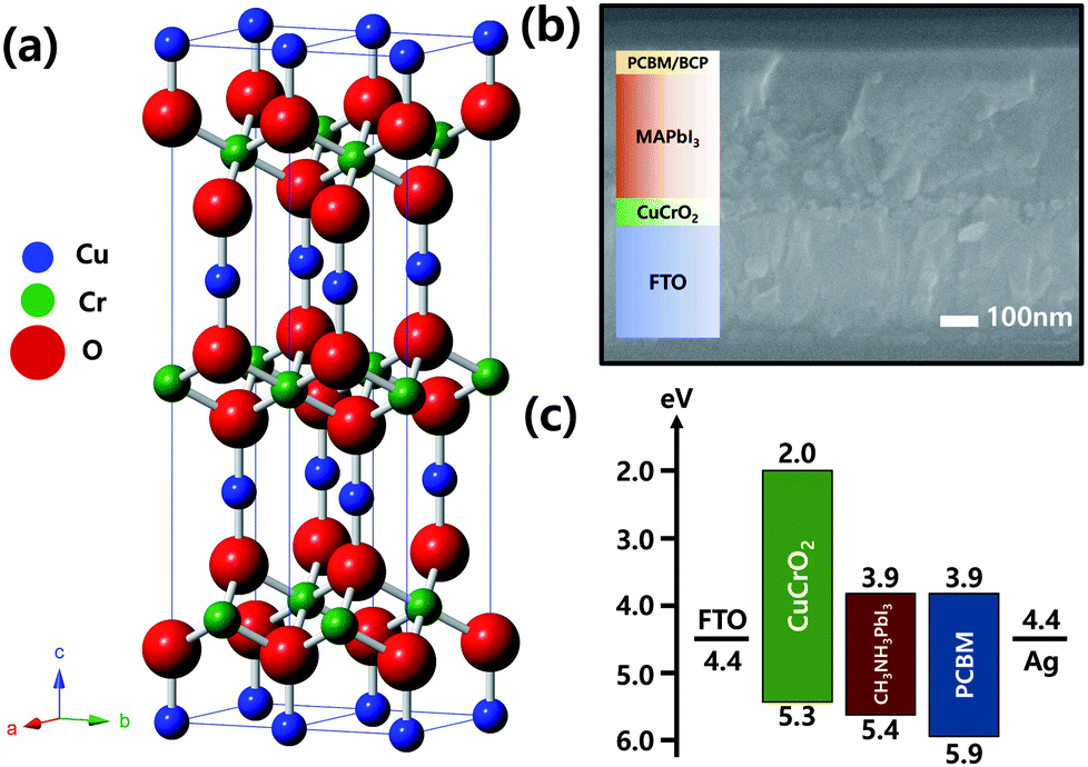 | ||
Fig. 1 (a) Illustration of crystal structure of delafossite compound (ABX2, space group: rhombohedral R![[3 with combining macron]](https://www.rsc.org/images/entities/char_0033_0304.gif) m). In case of CuCrO2, Copper ions are coordinated with the edges of octahedral oxygen ions that are formed with chromium ions (Cr(III)O6). Layered structure is organized by monovalent Cu layer and CrO6 octahedral layer. (b) Cross-sectional image of field emission-scanning electron microscopy (FE-SEM) showing completed PSCs. p-Type CuCrO2 and PCBM/BCP were used as hole and electron transporting layer, respectively. Each layer of CuCrO2, CH3NH3PbI3 and PCBM has the thicknesses of 40, 300 and 40 nm. And 100 nm thickness of Ag electrodes were deposited by thermal evaporation. (c) Energy band diagram of FTO/CuCrO2 nanoparticulates/CH3NH3PbI3/PCBM/BCP/Ag with p–i–n configuration showing valence and conduction band level alignment for the PSCs. m). In case of CuCrO2, Copper ions are coordinated with the edges of octahedral oxygen ions that are formed with chromium ions (Cr(III)O6). Layered structure is organized by monovalent Cu layer and CrO6 octahedral layer. (b) Cross-sectional image of field emission-scanning electron microscopy (FE-SEM) showing completed PSCs. p-Type CuCrO2 and PCBM/BCP were used as hole and electron transporting layer, respectively. Each layer of CuCrO2, CH3NH3PbI3 and PCBM has the thicknesses of 40, 300 and 40 nm. And 100 nm thickness of Ag electrodes were deposited by thermal evaporation. (c) Energy band diagram of FTO/CuCrO2 nanoparticulates/CH3NH3PbI3/PCBM/BCP/Ag with p–i–n configuration showing valence and conduction band level alignment for the PSCs. | ||
Fig. 2a and b are Transmission Electron Microscopy (TEM) images showing morphology and interplanar distance of individual CuCrO2 nanocrystals. The synthesized nanocrystals exhibit two forms of shape; one is as nanoplates with the average diameter of ∼20 nm and another as nanorods with the average size of 7 × 17 nm, respectively. SAED pattern in inset shows delafossite crystalline phase of CuCrO2 nanocrystals. In addition, the interplanar distance of 0.56 nm corresponds to the lattice spacing of 0.57 nm which between Cu–Cu ions originated from c-axis ((003) plane) of CuCrO2 delafossite structure.38 Fig. 2(c) shows XRD patterns one from as-prepared CuCrO2 and the other is from Mg doped CuCrO2. The XRD patterns are almost identical. Temperature and oxygen partial pressure during post-annealing process are critical to form pure CuCrO2 phase. Synthesized CuCrO2 nanocrystals are stable during low temperature annealing in air, however, it would be decomposed to secondary phases, i.e., CuO and CuCr2O4, in high temperature annealing. On the other hand, phase decomposition did not happen when high temperature annealing in Ar and the crystal growth has been observed.38,44 After synthesizing nanocrystals by the hydrothermal method, dispersing experiments were performed with different solvents44 as shown in Fig. S1.† Gradual aggregations of nanocrystals were observed in some solvents. After 30 hours, nanocrystals were well dispersed only in methanol. With methanol based dispersing solution, CuCrO2 layers were deposited onto FTO by spin-coating. Thickness of CuCrO2 layers was controlled by adjusting the number of coating. When spin-coated for 4, 10 and 15 times, the thickness of layers were achieved as 40, 50 and 70 nm, respectively. Fig. 2(d) shows planar-view SEM image of CuCrO2 nanocrystals deposited onto FTO. After the deposition of nanocrystals, post annealing treatments at 550 °C for 1 hour in Ar were performed to form solid networks between the nanocrystals.
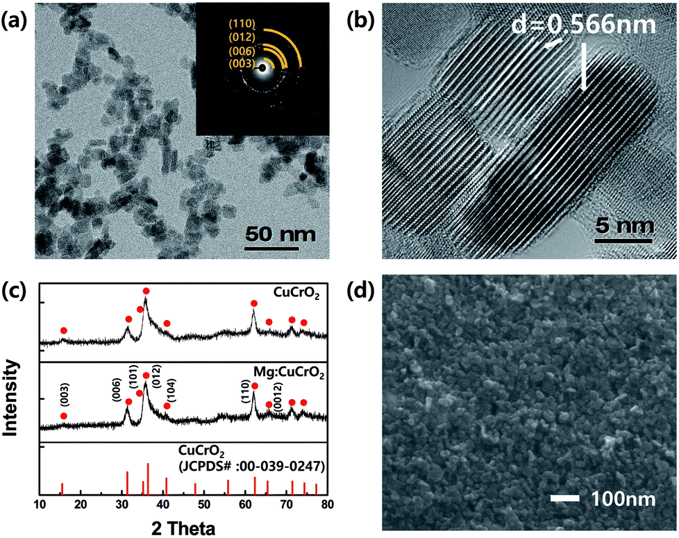 | ||
| Fig. 2 (a) TEM image of as-prepared CuCrO2 nanocrystals. Nanoplates and/or nanorods of the crystal can be observed and selected area electron diffraction pattern (SAED) as inset. (b) High-resolution TEM (HRTEM) image indicating interplanar distance about 0.56 nm corresponding to (003) plane of delafossite CuCrO2. (c) XRD patterns of CuCrO2 and Mg:CuCrO2 as-prepared nanocrystals showing crystallization into the identical delafossite structure. (d) Planar-view SEM image of CuCrO2 layer deposited onto FTO. | ||
Fig. 3 shows surface morphologies and their leakage current maps of the CuCrO2 nanoparticulate films obtained by atomic force microscopy (AFM) and conducting mode of AFM. Surface morphologies (Fig. 3(c), (e), and (g)) and leakage current maps (Fig. 3(d), (f), and (h)) of the CuCrO2 nanoparticulate films with the thickness of 30, 40, and 70 nm, were shown. The leakage current is clearly observed through the nanoparticulate films with the thickness of 30 and 40 nm as shown in Fig. 3(d) and (f). It is noted that the appreciable reduction in the leakage current in Fig. 3(h) indicating the complete coverage with the thickness of 70 nm.
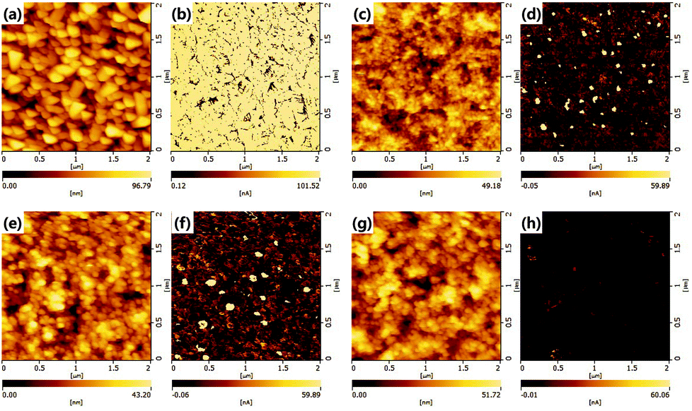 | ||
| Fig. 3 Surface morphology and leakage current map of bare FTO ((a) and (b)). Surface morphologies ((c), (e), and (g)) and leakage current maps ((d), (f), and (h)) of the CuCrO2 nanoparticulate films with the thickness of 30, 40, and 70 nm, respectively. The leakage current is clearly observed through the nanoparticulate films with the thickness of 30 and 40 nm as shown in Fig. 3(d) and (f). It is noted that the appreciable reduction in the leakage current in Fig. 3(h) indicating the complete coverage with the thickness of 70 nm. The surface roughness in RMS is about 16, 7.7, 6.9 and 9.2 nm for (a), (c), (e), and (g). All samples are measured in constant mode (force ref.: −0.5 nN, scan speed: 0.5 Hz, applied bias: 0.5 V). | ||
Fig. 4(a) shows Mott–Schottky measurement of CuCrO2 nanoparticulate films, and p-type semiconducting behaviour was confirmed by negative slope at a wide range of frequency from 1000 to 3000 Hz. The flat band potential of CuCrO2 was obtained by fitting from the measurement results with a value of 0.50 V versus standard calomel reference electrode (SCE) and of donor density with 4.28 × 1019 cm−3. We also further investigated the films by ultraviolet photoelectron spectroscopy (UPS) and Kelvin Probe Force Microscopy (KPFM) to obtain the information of electronic band structure with the work function. Fig. 4(b) shows the value of EF and Ecutoff located at 0.96 and 16.96 eV, and the work function of CuCrO2 is estimated to be 5.26 eV, and those of Mg:CuCrO2 is estimated 5.46 eV as shown in Fig. S2.† Fig. 4(c) shows the work function of CuCrO2 measured by KPFM with a value of 5.28 eV, which showed a good agreement with the result of UPS, indicating appropriate alignment with the valence band energy level of CH3NH3PbI3 (5.4 eV) and effective separation of photo-generated holes. Fig. 4(d) shows the optical transmittance spectra of CuCrO2 deposited on FTO with different thicknesses of ∼40, 50 and 70 nm, respectively, by using UV-Vis spectroscopy. Thin CuCrO2 layers having highly transparent property of 90% or more in visible light range are desirable to HTL, not absorbing the light reaching the perovskite photo-absorber. High transmittance is due to the large optical bandgap of CuCrO2 was calculated based on Tauc plot of the Kubelka–Munk transformation from the absorption spectra. The plot of α2 vs. hν in the inset and shows the direct optical bandgap of 3.36 eV, and that was measured to be 3.33 eV in case of Mg:CuCrO2 as shown in Fig. S3,† reasonably matched to values in the literature.39
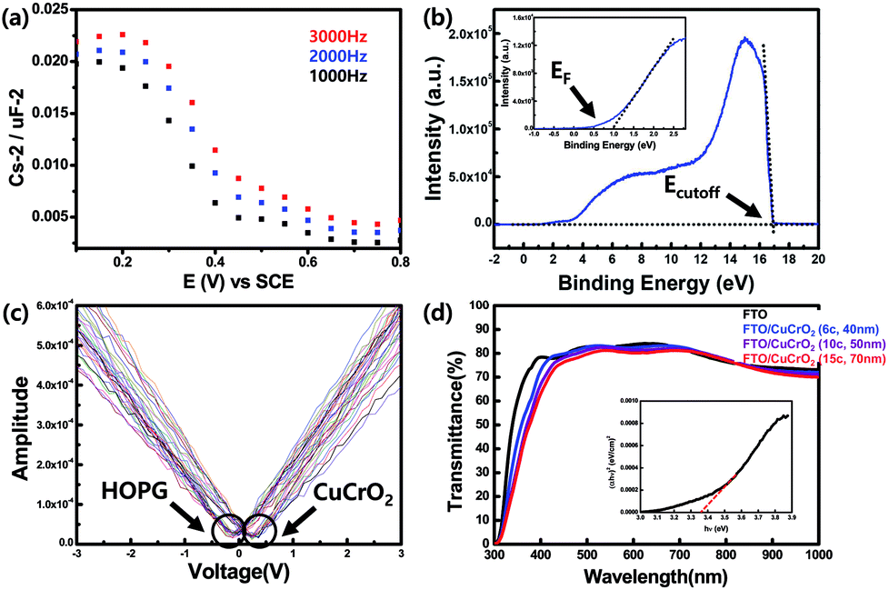 | ||
| Fig. 4 (a) Electrochemical Mott–Schottky plot of CuCrO2 particulate layers (post-annealed in Ar at 550 °C for 1 h) with frequency of 1, 2 and 3 kHz in the electrolyte of 0.5 M KOH with a standard calomel electrode, indicating a p-type characteristic. (b) Ultraviolet photoelectron spectroscopy (UPS) spectra of cutoff position (Ecutoff = 16.92 eV) of binding energy and position of kinetic energy of the electron (EF = 0.96 eV) in inset, using He(I) source (21.22 eV). The measured work function of CuCrO2 layer on FTO was 5.26 eV (vs. vacuum level). (c) Work function of the CuCrO2 nanocrystal particulate films measured by Kelvin probe force microscopy (KPFM) calibrated the cantilever with the surface of highly oriented pyrolytic graphite (HOPG). Each curve showing straight lines was measured by taking 25 randomly selected points on the nanocrystal particulate films and HOPG, work function was estimated to be 5.26 eV. (d) Optical transmittance spectra of air-baseline FTO and FTO/CuCrO2 layer with each thickness showing highly transparent at wide wavelength above 400 nm. Black line indicates a transmittance of FTO on to glass and blue, purple and red correspond with CuCrO2 layers of 6, 10 and 15 times of coating, respectively. The inset shows Tauc plot of absorption coefficient (α2) vs. photon energy (hν) to determine the band gap (Eg) indicating a value of direct optical bandgap of around 3.36 eV. | ||
With the delafossite CuCrO2 particulate HTLs, we fabricated PCSs. The resultant of current density (J) measured with respective to the applied voltage (V) under 1.5 AM illumination is shown in Fig. 5(a) and detailed parameters are listed in Table 1. To adjust thickness of CuCrO2 layers, we control the number of coating times 6, 10 and 15, corresponding to around 40, 50 and 70 nm in thickness, respectively. With the increase of CuCrO2 layer thicknesses, all the parameters (Jsc, Voc, and FF) PCE are decreased. The PCSs based on the 40 nm thick CuCrO2 HTL show the best performance in this study. The best PCE was ∼13.1%. We also measured the J–V curves using reverse as well as forward scans. In forward scan direction, slightly improved PCE with increased FF, despite a low degree of decreased in Jsc and Voc. Unlike the planar – type of inverted PCSs, all of our PSCs show appreciable hysteresis. It is simply because of high resistant CuCrO2 nanocrystals were used as HTLs. The incident photon to electron conversion efficiency (IPCE) spectrum (Fig. 5(b)) of PSCs based on CuCrO2 HTLs with different thicknesses exhibits an acceptable response in broad wavelength range from 400 to 750 nm. Decreased EQE spectra in relatively thick CuCrO2 layers are shown, resulting from reduced transmittance of light. In addition, integrated currents of IPCE over the full spectrum are calculated to be 17.5, 17.0 and 16.0 mA cm−2, respectively, which are well match with those obtained from the J–V curves. J–V curves of the fabricated PSCs based on different HTLs using CuCrO2, Mg:CuCrO2 and PEDOT:PSS as in inverted structure were measured shown in Fig. 5(c) and summarized in Table 2 with the champion performance of the cells. Devices based on CuCrO2 show relatively higher Voc than the devices on PEDOT:PSS, which verified more suitable alignment to valence energy level of CH3NH3PbI3 (5.4 eV) than PEDOT:PSS (5.2 eV).47 In addition, Voc of devices based on Mg:CuCrO2 was higher than that of CuCrO2, which related to deeper work function property resulted from UPS measurement data. Hole transporting materials with higher work-function, despite of the same device configuration and similar charge transporting property, exhibit higher Voc due to lower charge recombination rate.48 Steady-state photoluminescence (PL) spectra were measured to investigate effects on extracting photo-generated carriers from perovskite absorber when using different HTL. The PL measurement with the PSCs based on PEDOT:PSS is also carried out as a reference. CuCrO2 and Mg:CuCrO2 can effectively quench in the PL of CH3NH3PbI3 similar level to that of PEDOT:PSS, resulting in demonstrating that CuCrO2 can function as HTL material and have an advantage of replacing organic PEDOT:PSS.
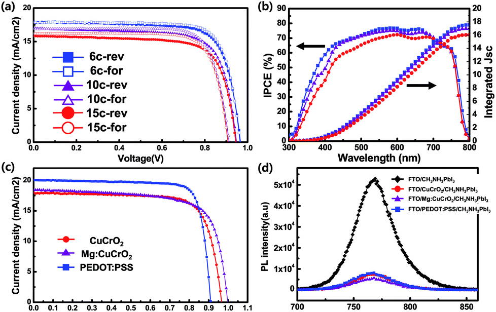 | ||
| Fig. 5 (a) J–V curves of perovskite solar cells based on different thicknesses of CuCrO2 layers measured under 1.5 AM illumination (100 mW cm−2). Each color of blue, purple and red corresponds to the thicknesses of CuCrO2 layers of about 40, 50 and 70 nm, respectively. The close and open symbols indicate J–V curves under reverse and forward bias, respectively. (b) IPCE spectra and integrated current density of devices. The open symbols of square and triangle indicate the calculated integrated current density. EQE and integrated Jsc of device based on thinner CuCrO2 layer increases to shorter wavelength (300–500 nm). (c) J–V characteristics of champion cells with different HTL materials. Each color of red, purple and blue indicates optimized CuCrO2, Mg:CuCrO2 and PEDOT:PSS based devices under reverse bias. (d) Photoluminescence spectra of devices based on different HTL materials that deposited on glass/FTO substrate with excitation at 464 nm. Each symbols (color) of diamond (black), circle (red), triangle (purple) and square (blue) indicate that without HTL, CuCrO2, Mg:CuCrO2 and PEDOT:PSS, respectively. | ||
| HTL | Jsc (mA cm−2) | Voc (V) | FF (%) | PCE (%) |
|---|---|---|---|---|
| CuCrO2 | 18.0 | 0.97 | 75.1 | 13.1 |
| Mg:CuCrO2 | 18.4 | 1.00 | 71.3 | 13.1 |
| PEDOT:PSS | 20.0 | 0.91 | 81.0 | 14.8 |
| Thickness of HTL | Scan direction | Jsc (mA cm−2) | Voc (V) | FF (%) | PCE (%) |
|---|---|---|---|---|---|
| 6c (40 nm) | Reverse | 18.0 | 0.97 | 75.1 | 13.1 |
| Forward | 17.9 | 0.96 | 78.5 | 13.4 | |
| 10c (50 nm) | Reverse | 17.0 | 0.95 | 73.4 | 11.9 |
| Forward | 16.9 | 0.91 | 78.2 | 12.0 | |
| 15c (70 nm) | Reverse | 15.8 | 0.95 | 73.5 | 11.0 |
| Forward | 16.2 | 0.91 | 77.3 | 11.4 |
In delafossite materials, Cu–Cu distance would be an important role of conductivity because holes are expected to hope from Cu to Cu along 3d-orbital and Cu–Cu distance is determined by MIII atoms. When divalent Mg is doped in CuCrO2, the dopants were located on trivalent Cr lattice site forming MgCr defect thermodynamically with lower formation energy, which are investigated by density functional theory.43 Thus Cu–Cu distance is decreased by Mg dopant, as ionic radius of Mg is smaller than that of Cr, leading to overlap of Cu d-orbital and resulting increase of charge mobility and conductivity.40 Ultimately, we speculated about the reason for slightly improved current density of PSCs based on Mg:CuCrO2.
Not only high photovoltaic performances, also air stability that is resistant to external environment is vital to practical application of PSCs. PSCs based on different HTLs were tested without any encapsulation in an ambient (at 26 °C and with 46–49% relative humidity in dark condition). The PCE of CuCrO2 and Mg:CuCrO2 based solar cell maintains above 80% of the initial value after 216 h of storage, on the other hand PCE of PEDOT:PSS based device decreased to < 60% of its initial value after 120 h of storage as shown in Fig. 6(a). A main reason of decreasing PCE is reduced FF (Fig. 6(d)) and Voc (Fig. 6(c)) before 168 h of storage times, in addition, Jsc of PEDOT:PSS based PSCs which was kept constant was abruptly decreased after 168 h, unlike CuCrO2 based PSCs shown in Fig. 6(b), and accordingly the PCE after 168 h was reduced. Decreased PCE occurred due to acidic and hygroscopic nature of PEDOT:PSS,24,49 since CH3NH3PbI3 is easily decomposed by humidity and react with acidic PEDOT:PSS50,51 and it was observed that it was decomposed into PbI2 which turned to yellow colour. The results show that CuCrO2 is suitable materials for HTL and makes the PSCs stable for external environment.
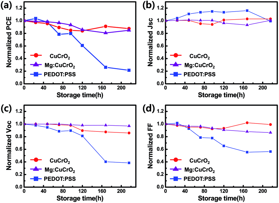 | ||
| Fig. 6 Stability of PSCs based on CuCrO2, Mg:CuCrO2, PEDOT:PSS without any encapsulation. Each symbol (color) of circle (red), triangle (purple) and square (blue) indicate that CuCrO2, Mg:CuCrO2 and PEDOT:PSS, respectively. 4-Main parameters of PCE (a), Jsc (b), Voc (c) and FF (d) were measured as a function of storage time (hours) in ambient atmosphere at 26 °C, 48% R.H. condition. | ||
Conclusions
We synthesized Cu based delafossite materials (CuCrO2 and Mg:CuCrO2) which have preferred crystal structure with p-type wide bandgap transparent conducting oxide (TCO) and they were applied as a HTL in p–i–n PSCs with FTO/CuCrO2(Mg:CuCrO2) layer/CH3NH3PbI3/PCBM/BCP/Ag configuration. CuCrO2 nanocrystals were synthesized by hydrothermal method have appropriate characteristic as a HTL in PSCs due to high optical transparency in broad wavelength of light and electrically well aligned valence band energy level to CH3NH3PbI3. In addition, inorganic material is more stable against external condition compared to conventional organic HTL (PEDOT:PSS). However, it is challenging to form thin, dense and uniform particulate layer by spin-coating, simply because of nanocrystal size and aggregation. To improve device performance, research on forming dense and uniform layer by synthesizing ultra-small sized nanocrystals and various coating method would be more desirable. Performance of devices was slightly improved by doping Mg, even though post annealing to form networking between nanocrystals was not processed, implying that it is applicable to flexible devices that cannot be subjected to high temperature heat treatment. As a result, CuCrO2 exhibit appropriate hole transporting materials with PCE of 13.1% and can be promising candidate for flexible devices.Conflicts of interest
There are no conflicts to declare.Acknowledgements
The authors acknowledge the Ministry of Science, ICT & Future Planning (MSIP) of Korea under contracts with NRF-2018K1A3A1A32055268, NRF-2018M3C1B7021994 and NRF-2016M3D1A1027664 through the National Research Foundation of Korea (NRF).Notes and references
- N. J. Jeon, J. H. Noh, Y. C. Kim, W. S. Yang, S. Ryu and S. I. Seok, Nat. Mater., 2014, 13, 897–903 CrossRef PubMed.
- Y. Zhao and K. Zhu, J. Phys. Chem. Lett., 2014, 5, 4175–4186 CrossRef PubMed.
- Y. Rong, Z. Tang, Y. Zhao, X. Zhong, S. Venkatesan, H. Graham, M. Patton, Y. Jing, A. M. Guloy and Y. Yao, Nanoscale, 2015, 7, 10595–10599 RSC.
- Y. Zhou, M. Yang, W. Wu, A. L. Vasiliev, K. Zhu and N. P. Padture, J. Mater. Chem. A, 2015, 3, 8178–8184 RSC.
- N. Ahn, D. Y. Son, I. H. Jang, S. M. Kang, M. Choi and N. G. Park, J. Am. Chem. Soc., 2015, 137, 8696–8699 CrossRef PubMed.
- NREL, Best Research-Cell Efficiencies, http://www.nrel.gov/pv/assets/images/efficiency-chart.png, 2017 (Rev. 10-30-2017).
- G. Giorgi, J. I. Fujisawa, H. Segawa and K. Yamashita, J. Phys. Chem. Lett., 2013, 4, 4213–4216 CrossRef PubMed.
- M. A. Green, A. Ho-Baillie and H. J. Snaith, Nat. Photonics, 2014, 8, 506–514 CrossRef.
- W. Y. Nie, H. H. Tsai, R. Asadpour, J. C. Blancon, A. J. Neukirch, G. Gupta, J. J. Crochet, M. Chhowalla, S. Tretiak, M. A. Alam, H. L. Wang and A. D. Mohite, Science, 2015, 347, 522–525 CrossRef PubMed.
- Y. Li, W. B. Yan, Y. L. Li, S. F. Wang, W. Wang, Z. Q. Bian, L. X. Xiao and Q. H. Gong, Sci Rep., 2015, 5, 14485 CrossRef PubMed.
- Z. Yang, A. Surrente, K. Galkowski, N. Bruyant, D. K. Maude, A. A. Haghighirad, H. J. Snaith, P. Plochocka and R. J. Nicholas, J. Phys. Chem. Lett., 2017, 8, 1851–1855 CrossRef PubMed.
- C.-H. Chiang, M. K. Nazeeruddin, M. Grätzel and C.-G. Wu, Energy Environ. Sci., 2017, 10, 808–817 RSC.
- V. Trifiletti, V. Roiati, S. Colella, R. Giannuzzi, L. De Marco, A. Rizzo, M. Manca, A. Listorti and G. Gigli, ACS Appl. Mater. Interfaces, 2015, 7, 4283–4289 CrossRef PubMed.
- X. Yin, M. Que, Y. Xing and W. Que, J. Mater. Chem. A, 2015, 3, 24495–24503 RSC.
- W. Chen, Y. Z. Wu, Y. F. Yue, J. Liu, W. J. Zhang, X. D. Yang, H. Chen, E. B. Bi, I. Ashraful, M. Gratzel and L. Y. Han, Science, 2015, 350, 944–948 CrossRef PubMed.
- X. Yin, P. Chen, M. Que, Y. Xing, W. Que, C. Niu and J. Shao, ACS Nano, 2016, 10, 3630–3636 CrossRef PubMed.
- S. Seo, I. J. Park, M. Kim, S. Lee, C. Bae, H. S. Jung, N. G. Park, J. Y. Kim and H. Shin, Nanoscale, 2016, 8, 11403–11412 RSC.
- S. S. Mali, H. Kim, S. E. Shim and C. K. Hong, Nanoscale, 2016, 8, 19189–19194 RSC.
- M. B. Islam, M. Yanagida, Y. Shirai, Y. Nabetani and K. Miyano, ACS Omega, 2017, 2, 2291–2299 CrossRef.
- S. Seo, S. Jeong, C. Bae, N. G. Park and H. Shin, Adv. Mater., 2018, 30, 1801010 CrossRef PubMed.
- A. E. Shalan, T. Oshikiri, S. Narra, M. M. Elshanawany, K. Ueno, H. P. Wu, K. Nakamura, X. Shi, E. W. Diau and H. Misawa, ACS Appl. Mater. Interfaces, 2016, 8, 33592–33600 CrossRef PubMed.
- A. Huang, L. Lei, Y. Yu, Y. Liu, S. Yang, S. Bao, X. Cao and P. Jin, Nanotechnology, 2017, 28, 20LT02 CrossRef PubMed.
- J. Ge, C. R. Grice and Y. Yan, J. Mater. Chem. A, 2017, 5, 2920–2928 RSC.
- W.-Y. Chen, L.-L. Deng, S.-M. Dai, X. Wang, C.-B. Tian, X.-X. Zhan, S.-Y. Xie, R.-B. Huang and L.-S. Zheng, J. Mater. Chem. A, 2015, 3, 19353–19359 RSC.
- W. Sun, S. Ye, H. Rao, Y. Li, Z. Liu, L. Xiao, Z. Chen, Z. Bian and C. Huang, Nanoscale, 2016, 8, 15954–15960 RSC.
- S. Ye, W. Sun, Y. Li, W. Yan, H. Peng, Z. Bian, Z. Liu and C. Huang, Nano Lett., 2015, 15, 3723–3728 CrossRef PubMed.
- Q. Xi, G. Gao, H. Zhou, Y. Zhao, C. Wu, L. Wang, P. Guo and J. Xu, Nanoscale, 2017, 9, 6136–6144 RSC.
- W. Sun, Y. Li, S. Ye, H. Rao, W. Yan, H. Peng, Y. Li, Z. Liu, S. Wang, Z. Chen, L. Xiao, Z. Bian and C. Huang, Nanoscale, 2016, 8, 10806–10813 RSC.
- C. Zuo and L. Ding, Small, 2015, 11, 5528–5532 CrossRef PubMed.
- L. Liu, Q. Xi, G. Gao, W. Yang, H. Zhou, Y. Zhao, C. Wu, L. Wang and J. Xu, Sol. Energy Mater. Sol. Cells, 2016, 157, 937–942 CrossRef.
- S. Chatterjee and A. J. Pal, J. Phys. Chem. C, 2016, 120, 1428–1437 CrossRef.
- Z.-L. Tseng, L.-C. Chen, C.-H. Chiang, S.-H. Chang, C.-C. Chen and C.-G. Wu, Sol. Energy, 2016, 139, 484–488 CrossRef.
- C. X. Guo, K. Sun, J. Ouyang and X. Lu, Chem. Mater., 2015, 27, 5813–5819 CrossRef.
- P. L. Qin, H. W. Lei, X. L. Zheng, Q. Liu, H. Tao, G. Yang, W. J. Ke, L. B. Xiong, M. C. Qin, X. Z. Zhao and G. J. Fang, Adv. Mater. Interfaces, 2016, 3, 1500799 CrossRef.
- H. Kawazoe, H. Yanagi, K. Ueda and H. Hosono, MRS Bull., 2000, 25, 28–36 CrossRef.
- W. C. Sheets, E. Mugnier, A. Barnabe, T. J. Marks and K. R. Poeppelmeier, Chem. Mater., 2006, 18, 7–20 CrossRef.
- F. A. Benko and F. P. Koffyberg, Mater. Res. Bull., 1986, 21, 753–757 CrossRef.
- D. Xiong, Z. Xu, X. Zeng, W. Zhang, W. Chen, X. Xu, M. Wang and Y.-B. Cheng, J. Mater. Chem., 2012, 22, 24760–24768 RSC.
- M. Yu, T. I. Draskovic and Y. Wu, Phys. Chem. Chem. Phys., 2014, 16, 5026–5033 RSC.
- R. Nagarajan, A. D. Draeseke, A. W. Sleight and J. Tate, J. Appl. Phys., 2001, 89, 8022–8025 CrossRef.
- G. Dong, M. Zhang, W. Lan, P. Dong and H. Yan, Vacuum, 2008, 82, 1321–1324 CrossRef.
- J. Tate, M. K. Jayaraj, A. D. Draeseke, T. Ulbrich, A. W. Sleight, K. A. Vanaja, R. Nagarajan, J. F. Wager and R. L. Hoffman, Thin Solid Films, 2002, 411, 119–124 CrossRef.
- D. O. Scanlon and G. W. Watson, J. Mater. Chem., 2011, 21, 3655–3663 RSC.
- J. Wang, Y.-J. Lee and J. W. P. Hsu, J. Mater. Chem. C, 2016, 4, 3607–3613 RSC.
- P.-L. Qin, Q. He, C. Chen, X.-L. Zheng, G. Yang, H. Tao, L.-B. Xiong, L. Xiong, G. Li and G.-J. Fang, Sol. RRL, 2017, 1, 1700058 CrossRef.
- D. Xiong, W. Zhang, X. Zeng, Z. Xu, W. Chen, J. Cui, M. Wang, L. Sun and Y. B. Cheng, ChemSusChem, 2013, 6, 1432–1437 CrossRef PubMed.
- Z. C. He, C. M. Zhong, S. J. Su, M. Xu, H. B. Wu and Y. Cao, Nat. Photonics, 2012, 6, 591–595 CrossRef.
- W. Yan, Y. Li, S. Ye, Y. Li, H. Rao, Z. Liu, S. Wang, Z. Bian and C. Huang, Nano Res., 2016, 9, 1600–1608 CrossRef.
- M. Jorgensen, K. Norrman and F. C. Krebs, Sol. Energy Mater. Sol. Cells, 2008, 92, 686–714 CrossRef.
- K. Chen, Q. Hu, T. Liu, L. Zhao, D. Luo, J. Wu, Y. Zhang, W. Zhang, F. Liu, T. P. Russell, R. Zhu and Q. Gong, Adv. Mater., 2016, 28, 10718–10724 CrossRef PubMed.
- T. H. Liu, K. Chen, Q. Hu, R. Zhu and Q. H. Gong, Adv. Energy Mater., 2016, 6, 1600457 CrossRef.
Footnote |
| † Electronic supplementary information (ESI) available. See DOI: 10.1039/c8ra02556h |
| This journal is © The Royal Society of Chemistry 2018 |