DOI:
10.1039/C8RA03027H
(Paper)
RSC Adv., 2018,
8, 26133-26143
Ultrafast nonlinear optical properties and carrier dynamics of silver nanoparticle-decorated ZnO nanowires
Received
9th April 2018
, Accepted 29th June 2018
First published on 20th July 2018
Abstract
Silver (Ag) nanoparticle-decorated zinc oxide (ZnO) nanowires (Ag–ZnO) have been successfully synthesized by chemical vapour deposition and the magnetron sputtering method. Scanning electron microscopy images indicate that Ag nanoparticles are distributed uniformly on the surface of the ZnO nanowires. The results of room temperature photoluminescence (RTPL) reveal two major emission peaks for the Ag–ZnO nanowires, and the emission peaks in the visible region are stronger than those of the unmodified ZnO nanowires. The mechanism of RTPL and low temperature photoluminescence (LTPL) emission is discussed in detail. Nonlinear optical properties and ultrafast dynamics have been investigated using the Z-scan and two color pump–probe (TCPP) techniques, respectively. The nonlinear absorption properties in the nano-, pico- and femto-second regime have been analyzed using the singlet state three-level and four-level models, respectively. The samples show self-focusing nonlinearity and good two-photon absorption (TPA)-induced ground state saturation absorption as well as excited state reverse saturable absorption behavior. For the nanosecond and picosecond pulses, the reverse saturated absorption in the excited state mainly originates from the absorption at low excited states or deep levels; however, for the femtosecond pulse, it is caused by the absorption at high excited states. The TCPP results show that the ground state or deep level light bleaching (for nano- and pico-second regime) and TPA-induced excited-state absorption (for femtosecond regime) behaviors range from 470 nm to 620 nm. The remarkable nonlinear optical properties reveal that Ag–ZnO nanowires are potential nanocomposite materials for the development of nonlinear optical devices.
1. Introduction
Up to now, various metal/nonmetal and semiconductor nanostructures have been successfully produced by different methods.1–3 Also, metal/nonmetal (such as noble metal, metal oxide and carbon)-doped or decorated semiconductors have been demonstrated with improved optoelectronic, photoelectrochemical and optical properties.4–8 Among various Group II–VI semiconductor materials, one dimensional nanostructures of ZnO possess advantages of large exciton binding energy of 60 meV and a wide direct band gap of 3.36 eV at room temperature; these properties make them promising for technological applications such as in light-emitting diodes, piezoelectric transducers, phosphors, sensors, UV lasers, solar cells, gas sensor optoelectronics, photovoltaics, photocatalysis, photonics, and UV photodetectors (PDs),9–12 where photoexcited carrier dynamic processes in the femtosecond to nanosecond timescales play a critical role.13,14
In recent years, a number of ultrafast optical techniques have been employed to investigate ultrafast nonlinear optical and carrier dynamics of organic and inorganic semiconductors;15–19 a variety of new metal and semiconductor nanocomposites have also been reported recently.20–22 Among them, the Ag nanoparticle-decorated ZnO (Ag–ZnO) nanostructures have been synthesized by various methods and technologies such as the low-temperature hydrothermal method,23 hydrothermal and chemical method,24 wet chemical synthesis and thermal evaporation process.25 The surface plasmon resonance (SPR) effect of a noble metal can expand the response range of incident light, increase optical absorption, enrich the electrode with light electrons increasing the light transmission rate, prolong the life of electronic devices and inhibit photoproduction of electron–holes in the composites.26–28 By decorating oxide photoanodes with Ag, the absorption of visible light is enhanced and the combination of photogenerated electron–holes is suppressed; however, the technological process is highly complex and requires high cost and also, large-scale applications are not possible because of vacuum-proof binders for printing technologies. Furthermore, to date, nonlinear optical properties and carrier dynamics of the Ag–ZnO nanowires have not been reported. In the present paper, the Ag–ZnO nanowire composites have been successfully synthesized; their morphology, structure and nonlinear optical properties are investigated. The results show that the samples have excellent structures and properties and thus, they are expected to have potential applications in photoelectric devices.
2. Experiment
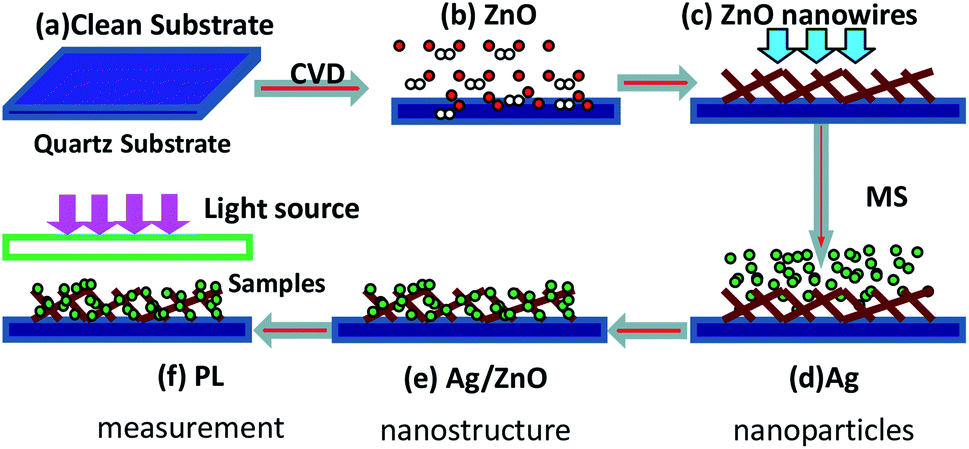
The Ag–ZnO nanowires were grown on quartz substrates by two-step chemical vapour deposition (CVD) and magnetron sputtering (MS) method. The schematic of the process is depicted in Scheme 1. The quartz substrate was cleaned ultrasonically in acetone, rinsed in deionized water and subsequently dried in flowing nitrogen gas before deposition. Then, the ZnO nanowires were grown by CVD, and Ag nanoparticles were deposited on the quartz substrates with ZnO nanowires by using the MS system.
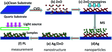 |
| | Scheme 1 Fabrication of the Ag–ZnO nanowires: (a) quartz substrate cleaned using the modified dip-coating method; (b) ZnO nanowires etched with Ar carrier gas; (c) as-deposited ZnO nanowires; (d) Ag nanoparticles produced for different sputtering times; (e) the Ag/ZnO nanostructure; (f) PL measurement. | |
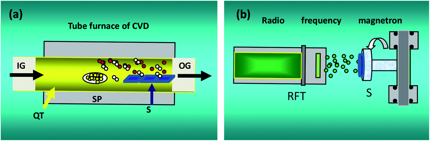
Fig. 1 shows the experimental setup for our CVD and MS systems. In Fig. 1(a), IG, OG and QT denote the input gas, output gas, quartz tube, respectively. SP and S are the source powder and substrates, respectively. In Fig. 1(b), RFT is a radio frequency target with a disc of Ag 60 mm in diameter and purity of 99.99%. S stands for substrates. ZnO (1 g) powder was used as the precursor, and it was placed in an alumina boat and loaded into the tubular furnace. The Au-coated quartz substrates were placed downstream from the powders. The furnace was heated to a preset temperature of 1250 °C. Ar was used as the carrier gas during growth at a constant flow rate of 100 sccm and pressure of 50 Pa. Then, the furnace was cooled down naturally to room temperature. During deposition, the base pressure in the deposition chamber and the radio frequency power were 6.0 × 10⁻⁴ Pa and 100 W, respectively. The sample was grown in an ambience with Ar sputtering at 20 sccm and a constant working pressure of 1.0 Pa.
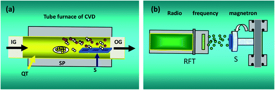 |
| | Fig. 1 Conceptual illustration for CVD and MS experiments. | |
The structural properties of Ag–ZnO and ZnO nanowires were observed by field emission scanning electron microscopy (FE-SEM). Crystallinity was analyzed using an X-ray diffractometer (XRD) equipped with monochromated Cu Kα irradiation. RTPL and LTPL spectra were obtained to study the optical properties of the samples; the excitation laser was a He – Cd laser with a wavelength of 325 nm, and the spectra were obtained from 350 nm to 800 nm. The nonlinear optical properties of Ag–ZnO nanowires were investigated by performing the femto-, pico- and nano-second Z-scans, as described previously.29–32 The samples were pumped at 532 nm by frequency-doubled 100 fs pulses from an amplified Ti-sapphire laser (1 kHz) and the second harmonic wavelengths of a pico- and nano-second Nd: YAG laser (Continuum Model YG 601, 50 Hz and 10 Hz), which provided pulses of about 21 ps and 4 ns. The output pulse energies from the laser system were 0.4 mJ, 0.6 mJ and 1.0 mJ for 4 ns, 3.0 J, 8.4 J and 16.8 J for 21 ps and 42.6 J, 58.4 J and 74.6 J for 100 fs with linear polarization. Time-resolved transient absorption spectra were recorded using a femtosecond two color pump–probe (TCPP) spectrometer, which has been described in detail elsewhere.33,34 Briefly, a Ti: sapphire laser system, same as the above-mentioned femtosecond Z-scan system, was used. The pump-induced absorption changes were probed over the range from 450 to 750 nm with a femtosecond white-light continuum generated in the sapphire plate. All experiments were performed at room temperature.
3. Results and discussion
3.1 Morphologies and structures of Ag–ZnO nanowires
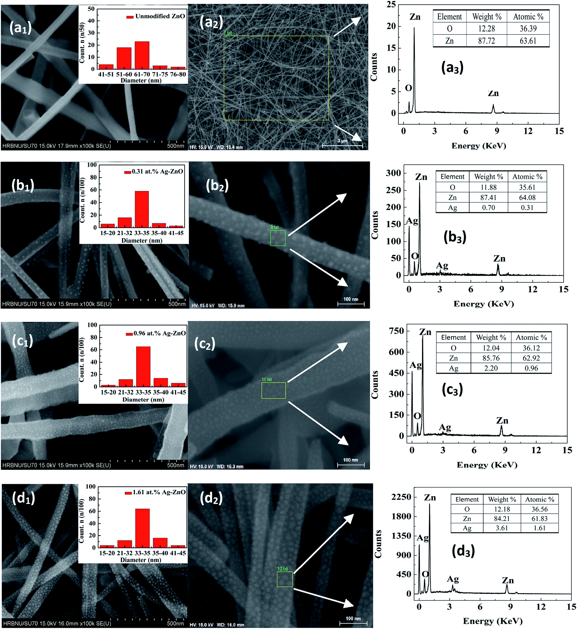
Fig. 2 (M1, M = a–d) shows the top-view FE-SEM images of the unmodified ZnO and Ag–ZnO nanowires grown on the quartz substrates. The inset of Fig. 2 (M1) shows the size distribution diagram of ZnO nanowires and Ag nanoparticles for each sample. The Ag–ZnO nanowires exhibited rougher surfaces because of the adsorption of Ag nanoparticles with the diameter of ∼34.86 nm (scale bar: 50 nm); Fig. 2 (M2) shows magnified SEM images of such structures. As the evaporation time was increased, the atomic percent of Ag gradually increased. A typical energy dispersive X-ray (EDX) spectrum of the Ag–ZnO nanowires is plotted in Fig. 2 (M3). Clear peaks of oxygen, Zn, and Ag were observed in EDX spectra. The EDX spectroscopy data confirmed that all samples contained 0.31%, 0.96% and 1.61% silver.
 |
| | Fig. 2 Top-view SEM images (a1–d1), magnified SEM images (a2–d2), EDX spectra (a3–d3) for Ag–ZnO nanowires with sputtering times of 0 s, 80 s, 100 s, and 120 s, respectively. | |
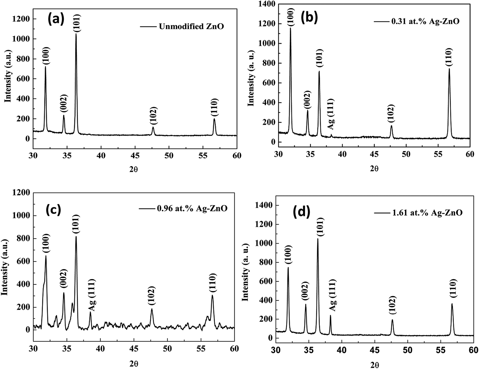
XRD analysis was carried out to investigate the structure of Ag–ZnO nanowires. As shown in Fig. 3(a–d), all patterns revealed a strong characteristic peak for the (002) plane of the ZnO hexagonal wurtzite structure. The other diffraction peaks were caused by the presence of Ag and Zn in the synthesized films. The peaks at two theta values of 38.24 degree could be assigned to the (111) plane of the face-centered-cubic structure of Ag. Therefore, these characteristic peaks appeared in the X-ray diffraction pattern due to the formation of a binary phase consisting of wurtzite ZnO and face-centered-cubic Ag.
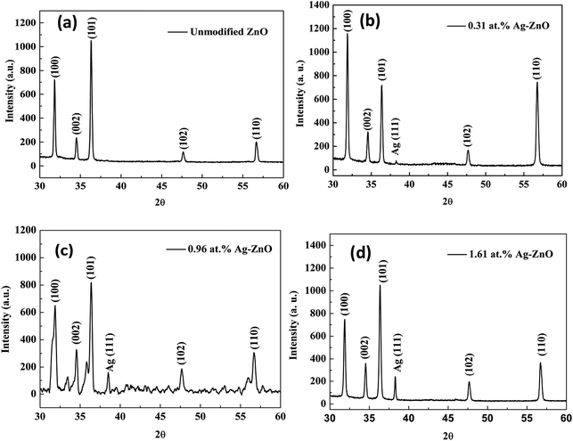 |
| | Fig. 3 XRD patterns (a–d) for Ag–ZnO nanowires with sputtering times of 0 s, 80 s, 100 s, and 120 s, respectively. | |
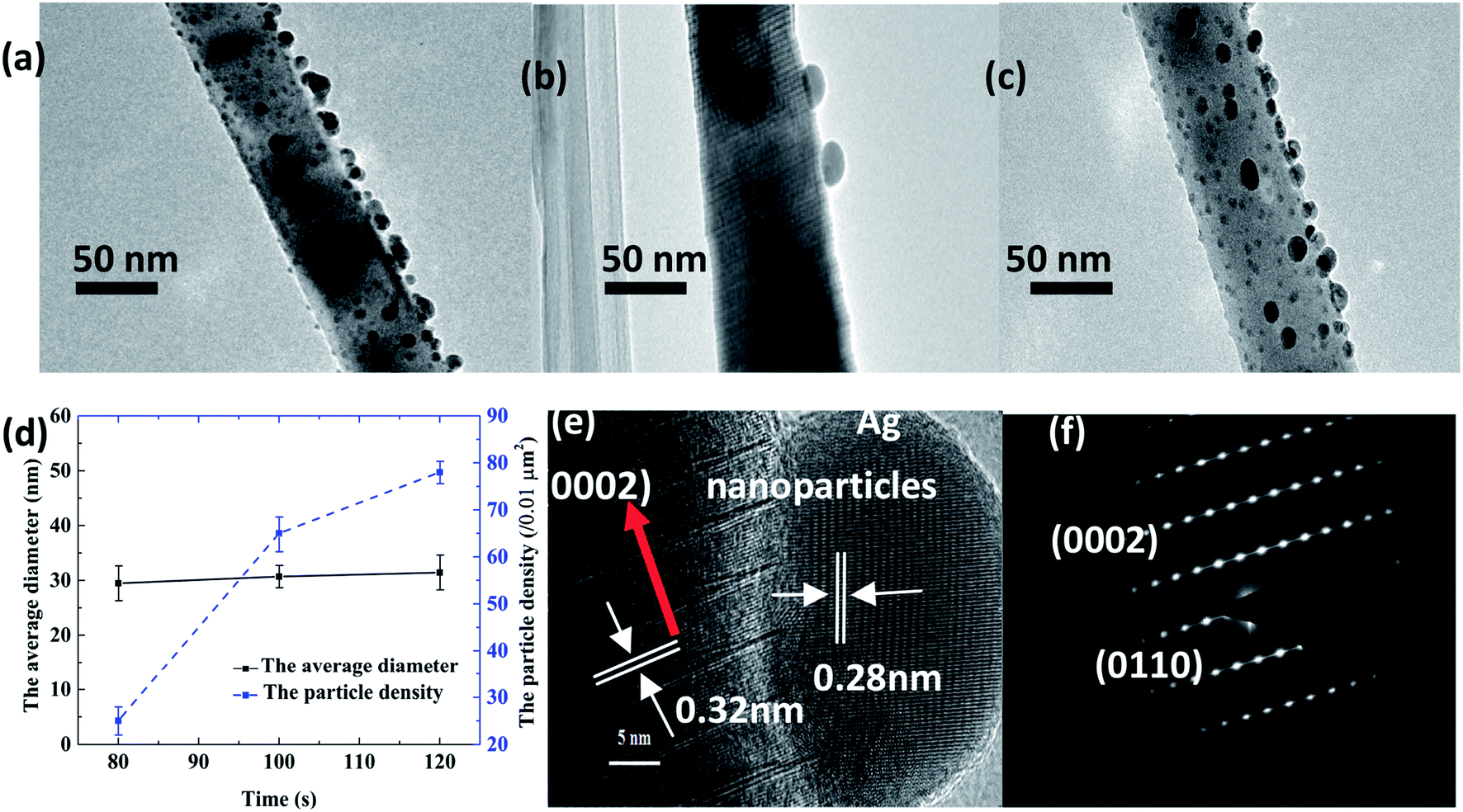
The TEM images of the Ag–ZnO nanowires synthesized at sputtering times of 80 s, 100 s, and 120 s are presented in Fig. 4(a–c), respectively. Fig. 4(d) shows that the average diameters of Ag nanoparticles for different times are similar, but the densities are different. Fig. 4(e) and (f) show the HRTEM and selected-area electron diffraction (SAED) patterns of the Ag–ZnO nanowires synthesized at 100 s, respectively. These results indicated that the ZnO nanowires with 0.32 nm space between the adjacent lattice planes had high crystal quality and were highly oriented to the c-axis direction of the 0002 crystal.
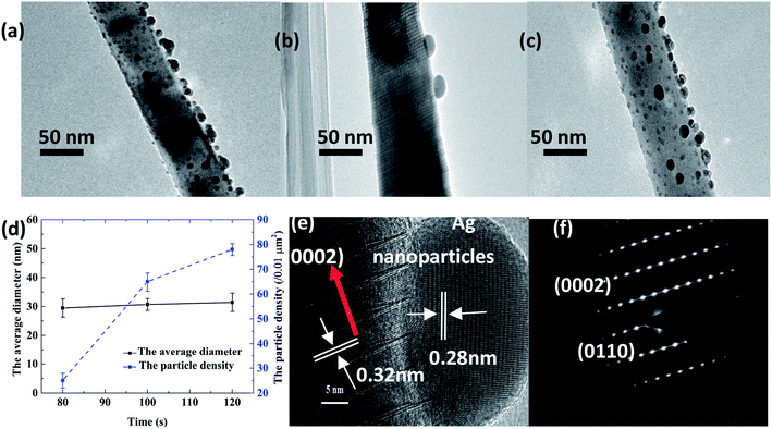 |
| | Fig. 4 TEM of Ag–ZnO nanowires with sputtering times of (a) 80 s, (b) 100 s, and (c) 120 s; (d) Average diameter and particle density of Ag–ZnO nanowires with sputtering times of 80 s, 100 s, and 120 s. HRTEM (e) and SAED image (f) of the Ag–ZnO nanowires for the sputtering time of 100 s. | |
3.2 Steady-state absorption spectra
The UV-visible spectra of Ag–ZnO nanowires prepared with different sputtering times are shown in Fig. 5. Clearly, all the samples exhibited strong linear absorption bands with a peak in the near-UV range (peak wavelength at 380, 378, 378 and 379 nm). The Ag–ZnO nanowires showed sharp absorptions at wavelengths slightly lower than 380 nm, and the addition of silver did not result in any significant difference in the band gap. Furthermore, silver-modified ZnO seed layer films with different contents of Ag were employed to corroborate the SPR absorption of Ag nanoparticle. The decoration of Ag nanoparticle induced band tail state in the Ag–ZnO nanowires.35 In comparison with the spectra of unmodified ZnO nanowires, the spectra of Ag–ZnO nanowires exhibited narrower peaks, and we found that the absorption rate of the Ag–ZnO nanowires was reduced.
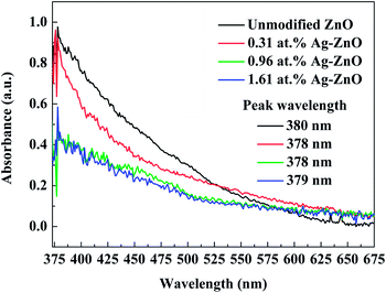 |
| | Fig. 5 UV-visible spectra of Ag–ZnO nanowires with sputtering times of 0 s, 80 s, 100 s, and 120 s. | |
3.3 RTPL and LTPL spectra of Ag–ZnO nanowires
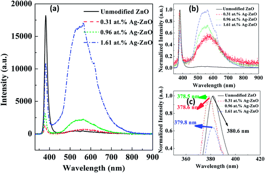
To study the PL characteristics, we recorded RTPL and LTPL spectra of unmodified ZnO and Ag–ZnO nanowires at different temperatures. Fig. 6(a) shows that all samples emitted strongly at 380.6, 378.6, 378.5 and 379.8 nm with sharp ultraviolet (UV) emission peaks (see Fig. 6(c)), corresponding to the near band edge (NBE) emission. Another broad peak in the visible range of 450–650 nm originated from the electron–hole recombination at a deep level (DL), which was caused by oxygen vacancy or zinc interstitial defects.36,37 After decoration with the Ag nanoparticles, the intensity of the visible emission peaks increased. According to some reports, this longer wavelength emission is due to the excitation caused by the recombination of photogenerated holes with singly ionized Ov site.37 The ultraviolet emission peaks are derived from the radiated composite luminescence of the forbidden band free excitons, and the peak of blue light emission is related to DL emission (for example, the electron transport from Zni leads to VZn electron transition luminescence), as reported in many papers.37,38 In Fig. 6(a), it can be clearly seen that the peak intensity ratio of DL emission to NBE emission follows the order Ag–ZnO nanowires > unmodified ZnO nanowires, which can be explained by a combination of a DL emission enhancing effect. The electron density of the Ag nanoparticles increased due to the transfer of electrons from the conduction band (CB) of ZnO nanowires to the Fermi level (FL) of Ag nanoparticles.38 In addition, it should also be pointed out that the DL emission peak of the unmodified ZnO nanowires was very weak compared to that of the Ag–ZnO nanowires. The electrons in the FL of Ag nanoparticles were excited due to surface plasmon resonance (SPR) of Ag nanoparticles upon interaction with the incident photon. These excited electrons may be transferred to the defect levels of ZnO. Since the FL of Ag nanoparticles is higher than the defect level of ZnO, the defect level electrons could recombine with the hole in the valence band of the ZnO nanowires. The ZnO PL band-edge enhancement due to both charge-transfer mechanisms and local-field mechanisms created a fundamental problem in studying the exciton–plasmon interactions using rough metal films as the source of plasmonic interactions. In Fig. 6(b) and (c), we can observe that the positions of the UV and visible emission peaks are slightly changed. The smaller blue shift in the UV emission resulted from the band-side excitation of the semiconductor, which generally occurs near the surface of the sample, resulting in uneven distribution of the excited carriers. To maintain a balanced and uniform distribution, excess unbalanced carriers diffused from the surface to the interior and simultaneously recombined due to radiative or non-radiative transition processes. Therefore, the majority of the excitations in the crystal were confined to the penetration depth of the photons below the surface. The red shift in the visible emission resulted from the intrinsic defects or/and Ag nanoparticles. Similar shifts in Ag/ZnO have been reported by L. Su et al.35 and M. Liu et al.40
 |
| | Fig. 6 PL (a) and normalized PL spectra (b and c) of unmodified ZnO and Ag–ZnO nanowires. | |
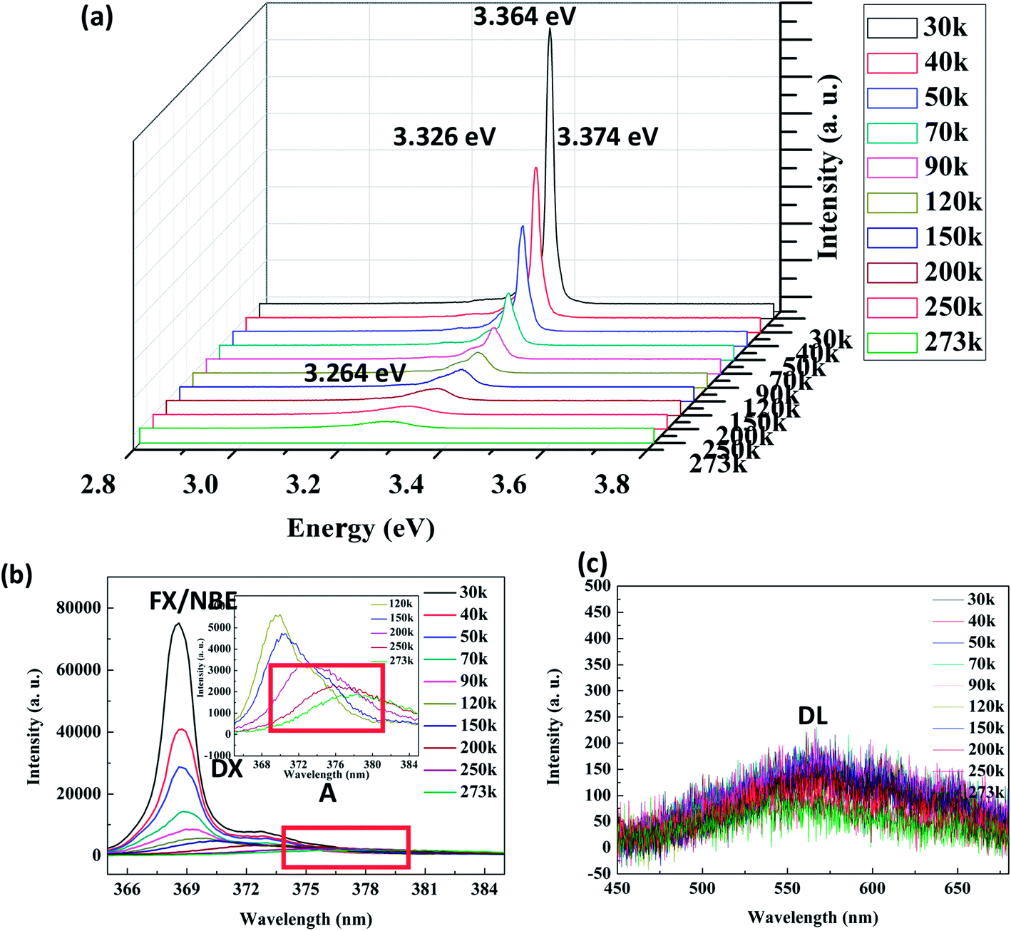
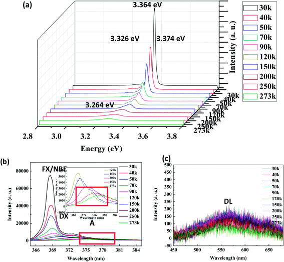
Fig. 7(a) shows the LTPL spectra of the Ag–ZnO nanowires in the range of 30–250 K. Each curve was fitted as a weighted sum of three components with centers at 3.374, 3.364, and 3.326 eV. The 3.376 eV peak is caused by free exciton (FX = NBE) recombination. The peaks at 3.364 and 3.326 eV can be due to bound excitons (DE). Similar results have been obtained by A. Amutha et al.38 for Ag-decorated ZnO nanorods, and a similar phenomenon has been obtained by H. P. He et al.39 for Al-doped ZnO. In addition, the LTPL spectra exhibit an NBE emission in the UV region (Fig. 7(b)) and DL emission in the visible region (Fig. 7(c)). At room temperature, the NBE emission peaks are observed at 3.264 eV (379 nm). In Fig. 7(b), we can see that with the increasing temperature, the intensity of the emission peak in the UV region decreases drastically. When the temperature exceeds 120 K, the dominant emission becomes an A line. As the temperature further increases, the first LO-phonon replica gradually merges into the A line, resulting in marked broadening of the NBE emission. The relative intensity of the DL emission peaks at about 2.20 eV is strongly reduced; the wavelength locations do not shift. No clear change is observed in the peak position of visible emission in the RTPL spectra.
 |
| | Fig. 7 LTPL spectra (a), ultraviolet (b) and visible (c) region spectra of Ag–ZnO nanowires with sputtering time of 120 s. | |
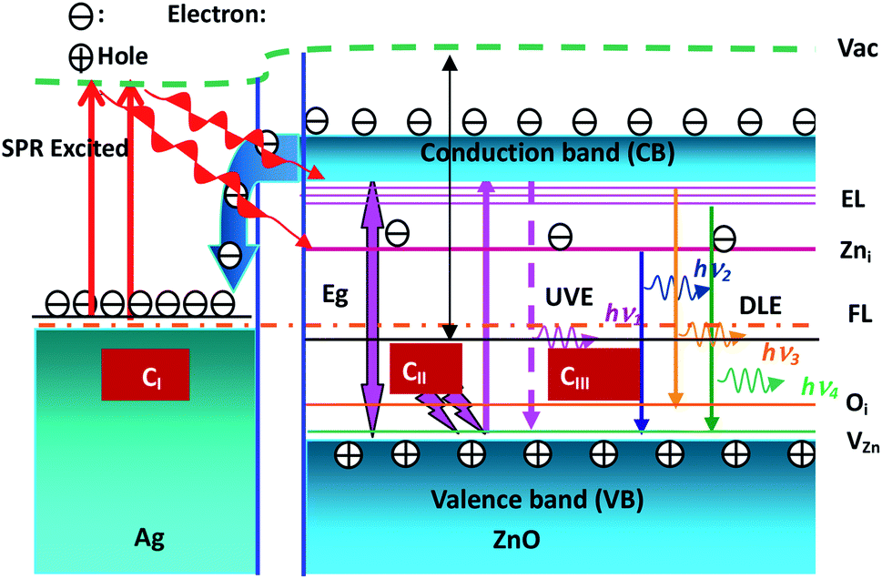
The ZnO band and the NBE and DL emissions are illustrated in Fig. 8. The process of electron dynamics can be explained as follows: the electrons get excited from the valence bands of ZnO nanowires to the conduction band by absorbing the incident laser photons, the near band edge (NBE) emission, and the electron transfer from the conduction band of ZnO nanowires to the Fermi level of Ag nanoparticles. These electrons are excited due to interactions between surface plasmon resonance (SPR) of Ag nanoparticles and the incident photons. These excited electrons may be transferred to the defect levels of ZnO. Since the Fermi level of Ag nanoparticles is higher than the defect level of ZnO, the defect level electrons can recombine with the hole in the valence band of ZnO nanowires. The visible emission peak is observed in the Ag–ZnO nanowire RTPL spectra. As shown in Fig. 8 (CII and CIII), all emission peaks can be analyzed by considering the energy band diagram. According to some reports, this long wavelength emission is excited by the recombination of photogenerated holes with the singly ionized oxygen vacancy sites.41–46 The UV emission peak is derived from the radiated composite luminescence of the forbidden band free excitons, and the peak of blue light emission originates from the electron transition from Zni to zinc vacancy (VZn) or from the Zni level to the top of the VB. As shown in Fig. 8 (CI), the electron density of Ag nanoparticles increases due to the transfer of electrons from the CB of ZnO nanowires to the Fermi level (FL) of Ag nanoparticles. These electrons are excited by the interactions between the SPR effects of Ag nanoparticles (around UV47) and the incident photons. These excited electrons may be transferred to the DL of ZnO nanowires, and they may recombine with the holes in the VB of ZnO nanowires since the FL of Ag nanoparticles is higher than the DL of ZnO. Therefore, the DL emission is enhanced in Ag–ZnO nanowires. Thus, as shown in Fig. 6(a), with the decorated Ag nanoparticles, the intensities of the visible emission peaks increase.
 |
| | Fig. 8 Illustration of the ZnO band (Eg), energy level (CB and VB) of ZnO, excitation levels (EL) defects (Zni, Oi and VZn), fermi levels (FL) of Ag, ultraviolet (UV) and deep-level (DL) emission. | |
For LTPL spectra, when the laser light (325 nm excitation) is incident on the Ag–ZnO nanowires, the electrons in the VB are excited to the CB. Then, the electrons in the CB of ZnO nanowires are transferred to the FL of Ag nanoparticles. Hence, the electron density increases in the FL of Ag nanoparticles. These electrons are excited and transferred to the bottom of the CB and recombine with the holes in the VB of ZnO nanowires, producing radiative emission. Therefore, the band edge emission increases when Ag nanoparticles are in contact with ZnO nanowires. The enhancement in PL emission is the combined effect of SPR of Ag nanoparticles coupled with both the excitons and defects in the ZnO nanowires.
3.4 The nonlinear optical properties of Ag–ZnO nanowires
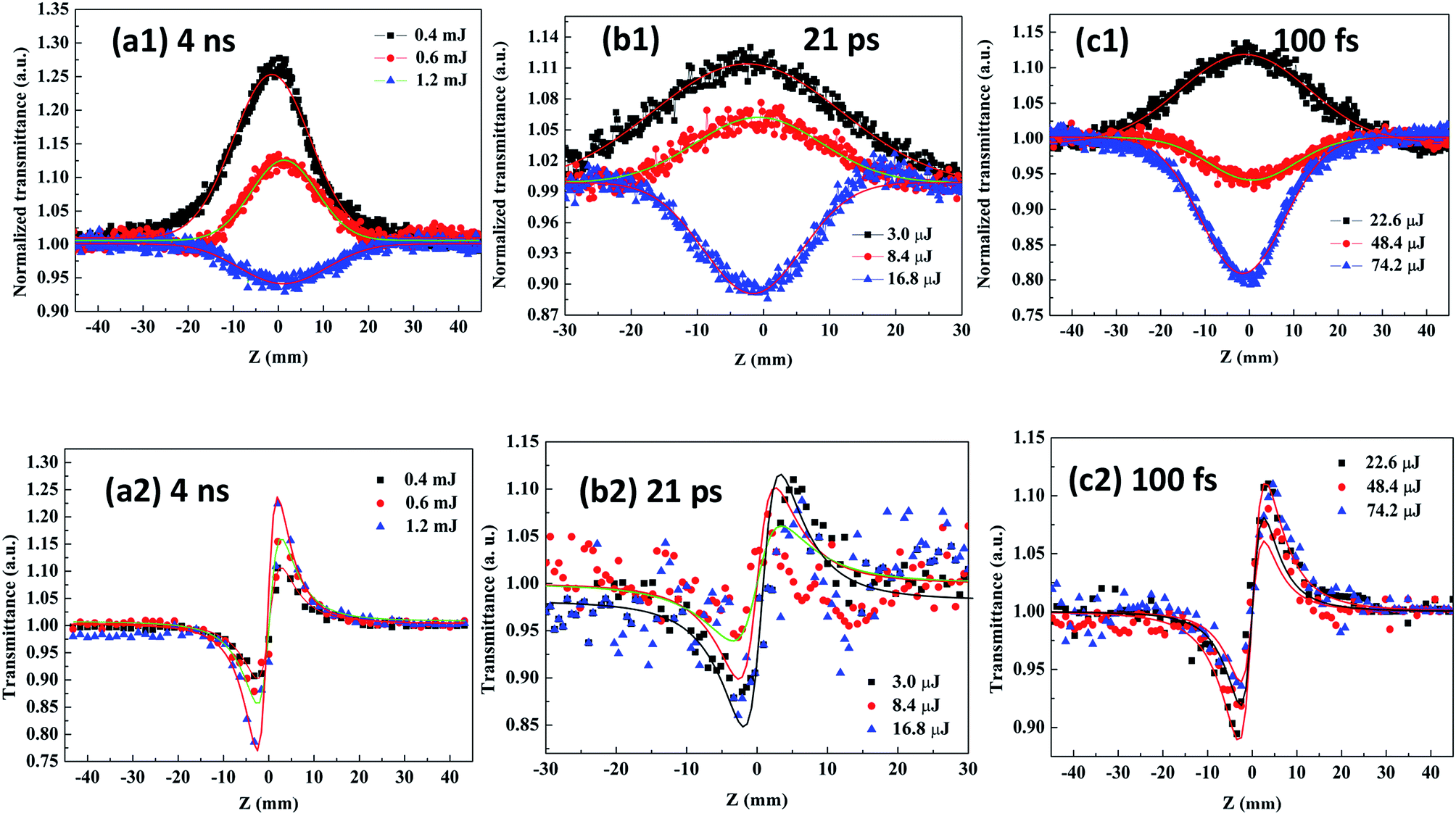
Fig. 9(a1–c1) and (a2–c2) show the curves of the open- and close-aperture Z-scans, respectively. It can be seen from the transmittance curve of the closed-aperture Z-scan that the signal profile has a valley followed by a peak, indicating positive (self-focusing) optical nonlinearity. The nonlinear absorption behavior of Ag–ZnO nanowires is revealed using a 532 nm laser irradiation; upon excitation, the CB was populated through the process of two-photon absorption (TPA). Because the laser excitation wavelength falls in the wing region of the exciton absorption, the condition for nonlinear absorption by TPA process (Eg/2 < ℏω < Eg, in Fig. 4) was satisfied by the TPA process and the strong absorption of the defect states. Under different laser energies, the Ag–ZnO nanowires exhibited different nonlinear absorption mechanisms. The low-energy Ag–ZnO nanowires displayed a normalized transmittance peak at the beam focus, indicating negative nonlinear absorption due to typical two – photon excitation-induced ground state saturable absorption (SA). However, the high-energy Ag–ZnO nanowires demonstrated a strong positive nonlinear absorption (reverse saturable absorption, RSA) in addition to SA, and the nonlinear absorption completely switched over to RSA. The change from SA to RSA near the focal region of the beam can be interpreted by considering the intensity-dependent contributions from SA and RSA. With an increase in the excitation power, the intensity of SA in the ground state reduced. When the excitation power was relatively large, a “valley” curve (near the focal point of the transmittance decreases), which is typical of the two – photon-induced excited state RSA effect, was obtained. The theoretical explanation of the mechanism of transformation is as follows: since the maximum power density of the probe beam occurred at the focal point of the lens, the nonlinear absorption of the sample was the strongest. For the two photon excitation-induced ground state SA, the electrons in the ground state were excited to the excited state; when there are no more electrons to absorb the extra photons, the phenomenon is called the “ground bleaching effect”. Therefore, the closer the focal point, the higher the transmittance, and it will appear as the “peak” in the measurement curve. In TPA-induced RSA, the sample first absorbed two photons at a time, which led to lower transmittance; the more closer it gets to the focal point, the more clear the effect, represented by the “valley” of the curve.
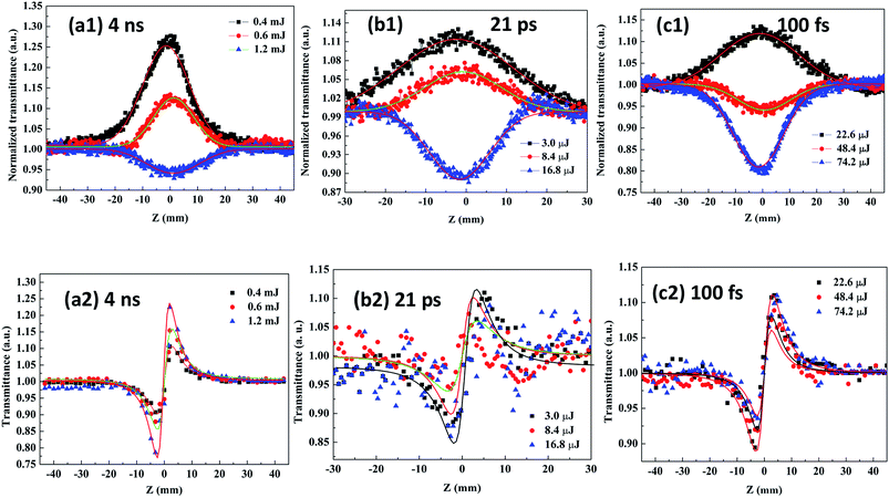 |
| | Fig. 9 Normalized open- (a1–c1) and closed- (a2–c2) aperture Z-scan transmittance curves of Ag–ZnO nanowires measured at 532 nm with 4 ns, 21 ps and 100 fs pulse width, respectively. | |
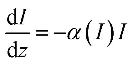
In the case of a thin saturable absorber, the optical intensity loss, as the beam propagates through the sample, is given by the relation48–50
| |
 | (1) |
where
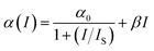
z is the propagation distance,
I is the incident intensity in the sample, and the total absorption coefficient
α(
I) is now given as
51,52| |
 | (2) |
where
α0 (
α0 = 4.37 cm
−1) is the linear absorption coefficient at the wavelength of excitation,
IS = (
hν/
σ0τ) is the saturation intensity,
hν is the photon energy, and
τ is the lifetime of the excited state. Saturation intensity is the intensity at which the absorption coefficient drops to half of its linear value.
β is the third order nonlinear absorption coefficient. The first term of
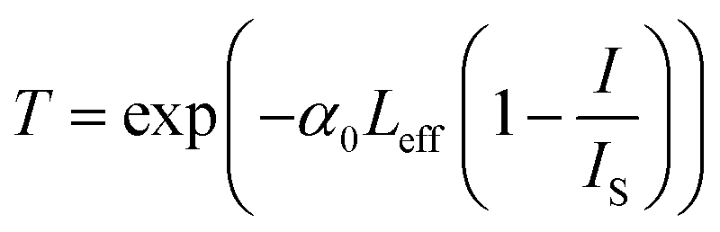
eqn (2) describes negative nonlinear absorption (SA); the second term describes positive nonlinear absorption (RSA) mediated by the excited state (include defect states), with relatively smaller contribution from TPA. The transmission of the saturable absorber is given by the equation
53–55| |
 | (3) |
The values of the nonlinear absorption and refractive index coefficients were expressed using the relation56–59
| |
 | (4) |
| | |
ΔTp-v = 0.406(1 − S)0.25|ϕ0|
| (5) |
where
q0(
z) =
βI0Leff/(1 +
z/
z0),
z0 is the Rayleigh range,
Leff = (1 − exp(−
α0L))/
α0 is the effective length with
L being the thickness of the sample. Δ
Tp-v is the measured peak-valley transmittance difference, Δ
ϕ0 =
kn2I0Leff is the on-axis phase-shift and
I0 is the incident intensity at focus.
S is the linear transmittance of the aperture given by
S = 1 − exp
![[thin space (1/6-em)]](https://www.rsc.org/images/entities/char_2009.gif)
−2(
ra/
wa)
2, where
ra is the radius of the aperture and
wa is the radius of the laser spot before the aperture. The values of
β and
n2 were evaluated by fitting the experimental data to
eqn (4) and
(5). The nonlinear absorption coefficients and nonlinear refractive index are shown in
Table 1. Due to the presence of Ag, the particles that were excited rapidly relaxed to the FL of Ag. In addition, the FL of Ag is higher than the FL of ZnO, making the electrons relax nonradiatively to the FL of ZnO and promoting RSA of the excited state. Similar analysis has been reported in many papers.
59–62 For example, M. T. Cisneros
et al.59 and R. Sato
et al.60 reported the nonlinear optical behavior of Ag nanoparticles in PMMA; Y. P. Chan
et al.61 and T. Voss
et al.62 reported the nonlinear optical properties of ZnO. Compared with the Ag nanoparticles or pure ZnO nanowires, the Ag–ZnO nanowires exhibited stronger nonlinear absorption. In contrast, the nonlinear absorption coefficient of the IZO nanowires was larger than the previously reported values of Ag nanoparticles and ZnO.
Table 1 Third-order nonlinear optical coefficients of Ag–ZnO nanowires at the laser pulse of 5 ns, 21 ps, and 100 fs, respectively
| Laser pulse |
β |
n2 |
| 4 ns |
−24.2, −42.5, 78.8 (cm GW−1) |
4.4, 5.2, 7.8 (× 10−17 m2 W−1) |
| 21 ps |
−32.8, −54.6, 104.3 (cm GW−1) |
4.7, 5.9, 8.9 (× 10−17 m2 W−1) |
| 100 fs |
−38.2, 68.5, 138.5 (cm GW−1) |
5.2, 7.4, 11.3 (× 10−17 m2 W−1) |
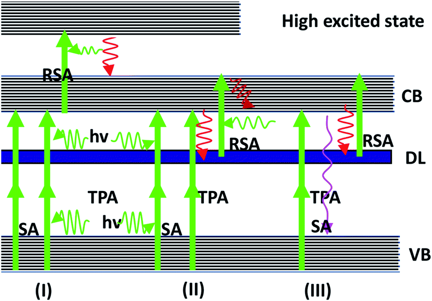
To discuss various parameters in the ns, ps and fs regimes that influence the RSA and SA, a general model of the multi-level energy diagram63,64 is used. For the nano- and pico-second laser pulses, three level models were adopted for analysis. Therefore, the nonlinear absorption mechanism of the Ag–ZnO nanowires can be explained by the repopulation of CB from the VB caused by TPA-induced ground state SA and TPA-induced low excited state (or DL) RSA. For the femtosecond laser, four level model analyses were carried out. The nonlinear absorption mechanism of the Ag–ZnO nanowires should be repopulation of CB from the VB caused by TPA-induced low excited state (or DL) SA and TPA-induced high excited state (CB) RSA. The above-mentioned process is shown in Fig. 10. The electrons get to the excited state from the ground state by absorbing the incident laser photons. These excited electrons relax to the S1 state in fs time scale by nonradiative decay. The excited electrons may also exhibit transitions to DL by the mechanism of nonradiative relaxation within the ps time scale. The electrons in DL can be further excited to the CB state. This process is known as the excited state absorption (ESA). On ps time scales, singlet–singlet transitions result in the ESA process.
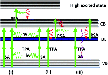 |
| | Fig. 10 Multi-level energy diagram showing VB and DL, CB and singlet high excited states, respectively. The solid lines and dashed lines represent optical excitation and nonradiative relaxation, respectively. | |
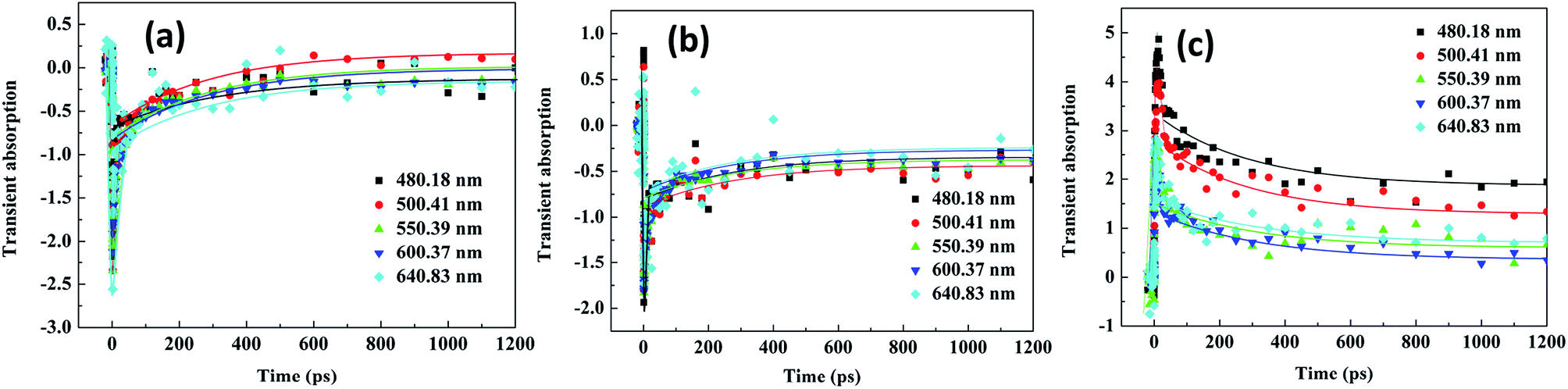
3.5 Transient absorption spectra of Ag–ZnO nanowires
Fig. 11 shows the TCPP experimental results. The samples were excited at different wavelengths (325, 380 and 400 nm) and probed at different wavelengths (480.18, 500.41, 550.39, 600.37, and 640.83 nm). The right panel shows the results at 325 nm; the middle and left panel show the results at 380 and 400 nm, respectively. The results in Fig. 11 are presented in the full time window up to 1.2 ns. This sample, was after being excited with 325 nm pump (Fig. 11(a)), displayed a very fast component with a time constant of few ps and a small amplitude slow decay component with a lifetime of few hundred ps. The fast component was due to electron–phonon coupling, whereas the slower decay was due to phonon relaxation. The excitation-transfer processes including the energy transfer between CB and internal conversion transition happened at the ps scale and led to the fast decay component in the pump–probe dynamics. The slow decay component corresponded to the evolution of excitation within internal conversion transition states. Upon direct excitation with the laser pump pulse at 325 nm, a negative signal was recorded for the ethanol solution of Ag–ZnO nanowires at different wavelengths (Fig. 11(a)). After excitation with 325 nm pumps and analyses as different wavelengths, the results obtained showed that Ag–ZnO materials have the same mechanism derived from ground state bleaching. This sample, when excited using a 380 nm pump (Fig. 11(b)), displayed the lifetime of the fast component; however, the lifetime varied in the range of 18–36 ps with the increasing probe wavelengths of 480.18, 500.41, 550.39, 600.37, and 640.83 nm, and a small amplitude slow decay component with a lifetime of >1.2 ns was also observed. The fast component was generated due to excited-state to DL coupling, and the slower decay was due to phonon relaxation. The excitation-transfer processes including the nonradiative transition from CB directly to the DL happened in the ps scale, leading to the fast decay component in the pump–probe dynamics. The slow decay component corresponded to the excitation from DL state directly to CB state without internal conversion transition states. Upon direct excitation with the laser pump pulse at 325 nm, a negative signal at different probed wavelengths (Fig. 11(b)) was recorded for the ethanol solution of Ag–ZnO nanowires. After excitation with 380 nm pumps and analyses with different wavelengths, the results showed that Ag–ZnO materials have the same mechanism, which is derived from bleaching of DL. After excitation with a 400 nm pump (Fig. 11(c)), a very fast component with a time constant of 12–26 ps and a small amplitude slow decay component with a lifetime of >1.2 ns were obtained. The fast component was due to the high excited-state to low excited-state coupling, whereas the slower decay was due to phonon relaxation. The excitation-transfer processes including the nonradiative decay from the high excited-state directly to a low excited-state led to the fast decay component in the pump–probe dynamics. The slow decay component corresponded to the evolution of excitation within the internal conversion transition states. Upon direct excitation with the laser pump pulse at 400 nm, a positive signal (Fig. 11(c)) was recorded for the ethanol solution of Ag–ZnO nanowires at different probed wavelengths. After excitation with 400 nm pump and analyses with different wavelengths, the obtained results showed that Ag–ZnO exhibits the same mechanism, which is derived from TPA-induced ESA.
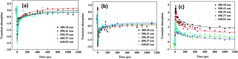 |
| | Fig. 11 Pump–probe transients of Ag–ZnO nanowires with sputtering time of 120 s excited at different wavelengths (325, 380 and 400 nm) and probed at different wavelengths. | |
4. Conclusions
In summary, we have investigated the structural properties, RTPL and LTPL spectra, and the ultrafast nonlinear optical properties and carrier dynamics of the Ag–ZnO nanowires. The average diameters of the Ag nanoparticles synthesized with different sputtering times are nearly the same although their densities are different. Moreover, the RTPL results demonstrate that the samples exhibit stronger visible emission peaks than the unmodified ZnO nanowires. The LTPL spectra show reduced emission, which can be due to re-absorption and scattering of the Ag nanoparticles. The self-focusing effect and nonlinear absorption behavior of Ag–ZnO nanowires in ethanol solution have been measured using the Z-scan technique. The TPA-induced ground state SA and excited state RSA behavior properties are evident from the experiments using three laser pulses. The ultrafast dynamics process is studied using a TCPP setup with a pulsed laser of 100 fs. The results indicate that the carrier dynamics depend strongly on the pump, the probe wavelengths and the bandgap of the material. The experimental results indicate that the few decade picosecond component has been assigned to vibrational relaxation in the excited electronic states, and the slow components represent the decay from S1 to the ground state (<1.2 ns) and DL to the ground state (>1.2 ns). These experimental results can be helpful for developing ultrafast optical switching and ultrafast devices for practical applications.
Conflicts of interest
There are no conflicts to declare.
Acknowledgements
The National Natural Science Foundation of China (11504072). University Nursing Program for Young Scholars with Creative Talents in Heilongjiang Province (No. UNPYSCT-2016179).
References
- D. Panda and T. Y. Tseng, J. Mater. Sci., 2013, 48, 6849–6877 CrossRef.
- Z. Li, G. Z. Wang, Q. H. Yang, Z. B. Shao and Y. Wang, Nanoscale Res. Lett., 2012, 7, 316 CrossRef PubMed.
- K. P. Jayadevan and T. Y. Tseng, J. Nanosci. Nanotechnol., 2005, 5, 1768 CrossRef PubMed.
- T. B. Guo, Y. Q. Chen, L. Z. Liu, Y. F. Cheng, X. H. Zhang, Q. Li, M. Q. Wei and B. J. Ma, J. Power Sources, 2012, 201, 408–412 CrossRef.
- S. M. Wang, Z. F. Li, P. Wang, C. H. Xiao, R. Zhao, B. X. Xiao, T. Y. Yang and M. Z. Zhang, CrystEngComm, 2014, 16, 5716–5723 RSC.
- J. Q. Liu, C. X. Guo, C. M. Li, Y. Y. Li, Q. B. Chi, X. T. Huang, L. Liao and T. Yu, Electrochem. Commun., 2009, 11, 202–205 CrossRef.
- P. Rauwel, M. Salumaa, A. Aasna, A. Galeckas and E. Rauwel, J. Nanomater., 2016, 2016, 19 Search PubMed.
- E. Rauwel, A. Galeckas, M. R. Soares and P. Rauwel, J. Phys. Chem. C, 2017, 121, 14879–14887 CrossRef.
- R. S. Devan, R. A. Patil, J. H. Lin and Y. R. Ma, Adv. Funct. Mater., 2012, 22, 3326–3370 CrossRef.
- Y. N. Xia, P. D. Yang, Y. G. Sun, Y. Y. Wu, B. Mayers, B. Gates, Y. D. Yin, F. Kim and H. Q. Yan, Adv. Mater., 2010, 15, 353–389 CrossRef.
- C. L. Hsu and S. J. Chang, Small, 2015, 10, 4562–4585 CrossRef PubMed.
- C. Soci, A. Zhang, B. Xiang, S. A. Dayeh, D. P. R. Aplin, J. Park, X. Y. Bao, Y. H. Lo and D. Wang, Nano Lett., 2007, 7, 1003 CrossRef PubMed.
- R. P. Prasankumar, P. C. Upadhya and A. J. Taylor, Phys. Status Solidi B, 2010, 246, 1973–1995 CrossRef.
- L. V. Dao, J. Davis, P. Hannaford, Y. H. Cho, M. A. Green and E. C. Cho, Appl. Phys. Lett., 2007, 90, 067401 Search PubMed.
- K. Makhal, S. Arora, P. Kaur, D. Goswami and K. T. Singh, J. Mater. Chem. C, 2016, 4, 9445–9453 RSC.
- M. A. M. Versteegh, T. Kuis, H. T. C. Stoof and J. I. Dijkhuis, Phys. Rev. B: Condens. Matter Mater. Phys., 2011, 84, 44 CrossRef.
- M. Montazeri, H. E. Jackson, L. M. Smith, J. M. Yarrison-Rice, J. H. Kang, Q. Gao, H. H. Tan and C. Jagadish, Nano Lett., 2012, 12, 5389 CrossRef PubMed.
- S. Gul, J. K. Cooper, C. Corrado, B. Vollbrecht, F. Bridges, J. H. Guo and J. Z. Zhang, J. Phys. Chem. C, 2011, 115, 20864–20875 CrossRef.
- B. P. Meh, J. R. Kirschbrown, M. M. Gabriel, R. L. House and J. M. Papanikolas, J. Phys. Chem. B, 2013, 117, 4390–4398 CrossRef PubMed.
- M. Joschko, P. Langlois, E. R. Thoen, E. M. Koontz, E. P. Ippen and L. A. Kolodziejski, Appl. Phys. Lett., 2000, 76, 1383–1385 CrossRef.
- K. Appavoo, M. Liu and M. Y. Sfeira, Appl. Phys. Lett., 2014, 104, 1424–1447 CrossRef.
- D. D. Wang, G. Z. Xing, X. Y. Wang, D. M. Yin, M. Zhou, Q. Guo, J. H. Yang, L. L. Yang, J. Cao and Y. S. Yan, Mater. Res. Bull., 2011, 46, 937–940 CrossRef.
- C. C. Yang, Y. K. Su, M. Y. Chuang, H. C. Yu and C. H. Hsiao, IEEE Trans. Electron Devices, 2015, 62, 2300–2305 Search PubMed.
- A. S. M. I. Uddin and G. S. Chung, Sensors, 2016, 1–4 Search PubMed.
- Y. H. Ko and J. S. Yu, Phys. Status Solidi A, 2012, 209, 297–301 CrossRef.
- J. X. Zhang and L. D. Zhang, Adv. Opt. Photonics, 2012, 4, 157–321 CrossRef.
- C. Zhang, H. Y. Xu, W. Z. Liu, L. Yang, J. Zhang, L. X. Zhang, J. N. Wang, J. G. Ma and Y. C. Liu, Opt. Express, 2015, 23, 15565 CrossRef PubMed.
- X. Zhang, Y. Liu and Z. Kang, ACS Appl. Mater. Interfaces, 2014, 6, 4480–4489 CrossRef PubMed.
- M. S. Bahae, A. A. Said and E. W. Van Stryland, Opt. Lett., 1989, 14, 955–957 CrossRef.
- R. Desalvo, M. Sheik-Bahae, A. A. Said, D. J. Hagan and E. W. Van Stryland, Opt. Lett., 1993, 18, 194 CrossRef PubMed.
- C. B. Yao, Y. D. Zhang, H. T. Yin, Q. Y. Meng, C. Q. Yu, J. Li and P. Yuan, Chem. Phys. Lett., 2013, 576, 35–38 CrossRef.
- C. B. Yao, Y. D. Zhang, J. Li, D. T. Chen, H. T. Yin, C. Q. Yu and P. Yuan, Opt. Mater., 2014, 37, 80–86 CrossRef.
- J. Takeda, K. Nakajima, S. Kurita, S. Tomimoto, S. Saito and T. Suemoto, Phys. Rev. B: Condens. Matter Mater. Phys., 2000, 62, 10083–10087 CrossRef.
- B. Li, R. Tong, R. Zhu, F. Meng, H. Tian and S. Qian, J. Phys. Chem. B, 2005, 109, 10705–10710 CrossRef PubMed.
- L. Su, N. Qin, W. Xie, J. H. Fu and D. H. Bao, J. Appl. Phys., 2014, 116, 561 Search PubMed.
- C. L. Hsu, Y. D. Gao, Y. S. Chen and T. J. Hsueh, ACS Appl. Mater. Interfaces, 2014, 6, 4277–4285 CrossRef PubMed.
- S. C. Lyu, Y. Zhang, H. Ruh, H. J. Lee, H. W. Shim, E. K. Suh and C. J. Lee, Chem. Phys. Lett., 2002, 363, 134–138 CrossRef.
- A. Amutha, S. Amirthapandian, B. Sundaravel, B. K. Panigrahi, K. Saravanan and P. Thangadurai, J. Appl. Phys., 2016, 120, 205104 CrossRef.
- H. P. He, H. P. Tang, Z. Z. Ye, L. P. Zhu, B. H. Zhao, L. Wang and X. H. Li, Appl. Phys. Lett., 2007, 90, 353 Search PubMed.
- M. Liu, S. W. Qu, W. W. Yu, S. Y. Bao, C. Y. Ma, Q. Y. Zhang, J. He, J. C. Jiang, E. I. Meletis and C. L. Chen, Appl. Phys. Lett., 2010, 97, 601 Search PubMed.
- K. Saravanan, B. K. Panigrahi, R. Krishnan and K. G. M. Nair, J. Appl. Phys., 2013, 113, 189 CrossRef.
- S. Agnihotri, S. Mukherji and S. Mukherji, RSC Adv., 2013, 4, 3974–3983 RSC.
- K. H. Tam, C. K. Cheung, Y. H. Leung, A. B. Djurisić, C. C. Ling, C. D. Beling, S. Fung, W. M. Kwok, W. K. Chan, D. L. Phillips, L. Ding and W. K. Ge, J. Phys. Chem. B, 2006, 110, 20865 CrossRef PubMed.
- H. P. He, Q. Yang, C. Liu, L. W. Sun and Z. Z. Ye, J. Phys. Chem. C, 2011, 115, 58–64 CrossRef.
- V. A. Fonoberov, K. A. Alim, A. A. Balandin, F. Xiu and J. Liu, Phys. Rev. B: Condens. Matter Mater. Phys., 2006, 73, 165317 CrossRef.
- A. Chernikov, M. Koch, B. Laumer, T. A. Wassner, M. Eickhoff, S. W. Koch and S. Chatterjee, Appl. Phys. Lett., 2011, 99, 979 CrossRef.
- S. K. Srivastava, P. Gangopadhyay, S. Amirthapandian, T. N. Sairam, J. Basu, B. K. Panigrahi and K. G. M. Nair, Chem. Phys. Lett., 2014, 607, 100–104 CrossRef.
- B. Gu, Y. Sun and W. Ji, Opt. Express, 2008, 16, 17745–17751 CrossRef PubMed.
- S. Perumbilavil, K. Sridharan, A. R. Abraham, H. P. Janardhanan, N. Kalarikkal and R. Philip, RSC Adv., 2016, 6, 106754–106761 RSC.
- B. Anand, R. Podila, P. Ayala, L. Oliveira, R. Philip, S. S. S. Sai, A. A. Zakhidov and A. M. Rao, Nanoscale, 2013, 5, 7271–7276 RSC.
- N. K. M. N. Srinivas, S. V. Rao and D. N. Rao, J. Opt. Soc. Am. B, 2003, 20, 2470–2479 CrossRef.
- A. E. Siegman, Lasers, University Science, Mill Valley, California, 1986, p. 207 Search PubMed.
- M. S. Malcuit, R. W. Boyd, L. W. Hillman, J. Krasinski and C. R. Stroud, J. Opt. Soc. Am. B, 1984, 1, 73–75 CrossRef.
- M. Samoc, A. Samoc, B. L. Davies, H. Reish and U. Scherf, Opt. Lett., 1998, 23, 1295–1297 CrossRef PubMed.
- C. B. Yao, X. Wen, Q. H. Li, X. Y. Yan, J. Li, K. X. Zhang, W. J. Sun, L. N. Bai and S. B. Yang, Chem. Phys. Lett., 2017, 671, 113–117 CrossRef.
- F. J. Zhang, W. F. Guo, X. B. Sun, Q. Ren, Y. Gao, H. L. Yang, G. H. Zhang, Y. T. Chow and D. Xu, Laser Phys. Lett., 2010, 4, 230–233 CrossRef.
- B. S. Kalanoor and P. B. Bisht, Opt. Commun., 2010, 283, 4059–4063 CrossRef.
- S. Ijaz, A. Mahendru and D. Sanderson, IEEE J. Quantum Electron., 1990, 26, 760–769 CrossRef.
- M. T. Cisneros, N. Yanagihara, B. G. Rolon, M. A. M. Nava, O. G. I. Manzano, D. A. M. Arrioja, J. S. Mondragon, E. A. Gomez and L. A. A. Cortes, Microelectron. J., 2009, 40, 621–623 CrossRef.
- R. Sato, M. Ohnuma, K. Oyoshi and Y. Takeda, Phys. Rev. B: Condens. Matter Mater. Phys., 2014, 90, 125417 CrossRef.
- Y. P. Chan, J. H. Lin, C. C. Hsu and W. F. Hsieh, Opt. Express, 2008, 16, 19900–19908 CrossRef PubMed.
- T. Voss and J. P. R. A. Dev, Phys. Status Solidi B, 2010, 247, 2476–2487 CrossRef.
- E. Parilov and M. J. Potasek, J. Opt. Soc. Am. B, 2006, 23, 1894–1910 CrossRef.
- G. H. Fan, Y. H. Han, S. L. Luo, Y. T. Li, S. L. Qu, Q. Wang, R. X. Gao, M. R. Chen and M. Han, Phys. Chem. Chem. Phys., 2016, 18, 8993–9004 RSC.
|
| This journal is © The Royal Society of Chemistry 2018 |
Click here to see how this site uses Cookies. View our privacy policy here. 
 Open Access Article
 This Open Access Article is licensed under a Creative Commons Attribution-Non Commercial 3.0 Unported Licence
 *,
Xing Wen,
Qiang-Hua Li and
Wen-Jun Sun
*,
Xing Wen,
Qiang-Hua Li and
Wen-Jun Sun