
 Open Access Article
 This Open Access Article is licensed under a Creative Commons Attribution-Non Commercial 3.0 Unported Licence
Wide channel broadband CH3NH3PbI3/SnS hybrid photodetector: breaking the limit of bandgap energy operation†
Mohit Kumarab,
Hong-Sik Kimabc,
Dae Young Parkc,
Mun Seok Jeongc and
Joondong Kim *ab
*ab
aPhotoelectric and Energy Device Application Lab (PEDAL), Multidisciplinary Core Institute for Future Energies (MCIFE), Incheon National University, 119 Academy Rd. Yeonsu, Incheon, 22012, Republic of Korea. E-mail: joonkim@incheon.ac.kr
bDepartment of Electrical Engineering, Incheon National University, 119 Academy Rd. Yeonsu, Incheon, 22012, Republic of Korea
cDepartment of Energy Science, Sungkyunkwan University, Suwon 16419, Republic of Korea
First published on 26th June 2018
Abstract
Perovskite-based hybrid organic–inorganic devices have recently demonstrated high potential in optoelectronics. Yet, the preparation of perovskite-based photodetectors over a desired scale without any complex architecture is still challenging. Herein, we proposed a new CH3NH3PbI3/SnS hybrid planar broadband (365 to 850 nm) photodetector, having a wide channel length of 6 mm. The growth of the device was studied by utilizing scanning electron microscopy, energy-dispersive X-ray mapping, X-ray diffraction, and optical spectroscopies. Furthermore, the efficient charge transfer from CH3NH3PbI3 to SnS was confirmed by employing time-correlated single photon counting. The pure SnS device generates 0.05 μA photocurrent at 365 nm, 4 mW cm−2, which is notably enhanced 140 times after embedding with CH3NH3PbI3. Further, the hybrid device shows a significant photoresponse even below the band gaps of individual CH3NH3PbI3 or SnS, which matches well with the density functional theory prediction. The observed results will create new opportunities to develop and design a low-cost, broadband, and efficient photodetector over a chosen horizontal area.
1. Introduction
Converting light into electrical signal is the fundamental processes of a photodetector, which is essential for most of the optoelectronic applications such as communication, video imaging, biochemical sensors, night vision, and many other industrial fields.1–5 Therefore, it remains always of great interest to the scientific community to design an improved photodetector with convenient fabrication processes.1,5–7 A perovskite-based photodetector is expected to fulfill most of the crucial requirements because of its tunable bandgap, high optical absorption, very long diffusion length.2–5,8–10 Particularly, in the past few years, varieties of perovskite-based photodetectors have been design with vertical and lateral (horizontal) configurations.1,6 Nevertheless, it remains a challenge to realize a high-performing perovskite photodetector with a lateral structure over a desirable area.To this end, perovskites purely and along with other materials such as graphene,11 layered MoS2,12 WS2,13 and WSe2 (ref. 14) have been integrated to design novel optoelectronic devices with tailored and improved photoresponse properties. Unfortunately, most of them are on micro-size channel length and the fabrication must undergo extremely complex and precise processes. For example, chemical vapor deposition synthesized 2D nanosheets must transfer onto a designated substrates.1,15–17 On the other hand, it is practically difficult to have a large area (>1 mm2) 2D nanosheets by exfoliation and in addition, photolithography should be implemented to design optoelectronic device.1,12,18 These processes are not very suitable for large area device fabrication. Although, various large area single crystal perovskites-based photodetectors have been demonstrated. Yet, designing of the thin film-based large area perovskite photodetector is hitherto unexplored for an efficient photodetection.
Recently, it is reported that the layered SnS and CH3NH3PbI3 forms a van der Waals heterostructure, which was predicted as a superior junction for photodetection.19 The integration of these two materials, therefore, offers opportunities to understand unique charge transfer mechanisms and light matter interactions for the application of photodetector, even below the individual band gaps.
In this study, we have fabricated large area CH3NH3PbI3/SnS hybrid broadband lateral (horizontal) photodetector by employing sputtering and solution-processed methods. The growth of the device was confirmed by scanning electron microscopy (SEM), energy-dispersive X-ray (EDS) mapping, X-ray diffraction (XRD), and optical absorbance spectroscopy. The fast carrier life time obtained by time correlation single photon counting (TCSPC) revealed the true charge carrier dynamic across the junction. The hybrid device shows 20 times faster photoresponse and 140 times enhanced photocurrent, compared to that of the pure SnS device. The presented results will be useful to design high-performing perovskites-based hybrid photodetector over a desired area by conventional and affordable approaches.
2. Experimental details
2.1. Materials
Perovskite precursors, MAI (methylammonium iodide) and PbI2 (Lead(II) iodide, 99.99%) were purchased from Greatcell Solar Ltd. and Alfa, respectively. Organic solvents, DMF (N,N-dimethylformamide, anhydrous, 99.8%) and DMSO (dimethyl sulfoxide, anhydrous, 99.9%) were received from Sigma Aldrich.2.2. X-ray diffraction
Powder X-ray diffraction (PXRD) was performed on an X-ray diffractometer (Rigaku, SmartLab) using Cu-Kα radiation (λ = 1.54059 Å). Bragg–Brentano focusing was performed at 45 kV and 200 mA with a tube.2.3. UV-Vis spectroscopy and study state photoluminescence (PL) spectroscopy
A V-670 UV-Vis/NIR spectrophotometer (JASCO) was used in reflectance mode at room temperature with an integrating sphere; the range evaluated was 400–900 nm. A barium sulfate plate was used as the standard (100% reflectance). The reflectance data were converted to absorbance for calculation Kubelka–Munk equation presented below, where α, S, and R are the absorption, scattering coefficient, and reflectance, respectively, α/Ѕ = (1 − R)2/(2R). The absorbance of SnS and hybrid device were performed using an ultraviolet-visible-near-IR spectrophotometer (Shimadzu, UV-2600). The steady-state PL spectra of the perovskite film were collected using an NTEGRA spectra instrument with a 355 nm laser excitation source.2.4. Time correlated single photon counting
Room temperature time resolved a photo luminance (TRPL) measurement was performed by using time correlated single photon counting (TCSPC) technique with a Microtime-100 (Picoquant) system. The solid-state laser excitation wavelength of 405 nm, at a repetition rate of 40 MHz and a laser pulse width shorter than 25 ps is used to perform the measurements.2.5. Device fabrication and tested
The top ITO layer (∼300 nm) was deposited at 300 °C using ∅ 4-in DC magnetron sputtering. A DC power of 3.7 W cm−2 was applied to the ITO target under an Ar flow of 50 sccm. The Kapton tape was used to prepare the masks. The SnS layers were deposited using a 99.999% pure amorphous SnS2 target (iTASCO, TSNALT0027, ∅ 2-inch). Prior to depositing the SnS layers, various substrate temperatures and working pressures were used to reduce sulfur from the sputtered SnS2 flux. The optimized temperature, i.e., 300 °C, and sputtering power, i.e., 50 W, were used for deposition in the presence of flowing Ar gas (30 sccm) with a deposition pressure of 6 m torr. The optimized growth conditions are mentioned in ref. 20 and 21. A base pressure of 3 × 10⁻⁶ torr was achieved prior to the flow of the Ar gas. A deposition time of 10 minutes was kept constant. 1 M MAPbI3 perovskite solution was prepared by dissolution of equimolar MAI and PbI2 in DMSO/DMF (1/4, v/v) with continuously stirring for overnight and then solution was filtered with PTFE syringe filter (0.2 μm). MAPbI3 film was fabricated with conventional spin coating method. Solution was spin-coated on glass substrate at 3000 rpm for 30 s and then annealed 100 °C for 10 minutes. Similar fabrication processes were also performed on SnS layers. As a result, the overall thickness of the perovskite/SnS device was around 600 nm. The cross section of the device and morphology of the SnS layers were studied using a field emission electron microscope (FESEM, JEOL, JSM_7800F). Different light sources starting from ultraviolet (365 nm) to near-infrared (850 nm) were used in the photoresponse measurements. The both ITO contacts were connected to the positive and the negative terminals of the source measure unit (SMU), respectively. The transient photoresponse of the device was studied by the chronoamperometry method under pulsed monochromatic light by varying the bias and light intensity. A function generator (MFG-3013A, MCH instruments) was applied to the light source. Light intensity was calibrated using a power meter (KUSAM-MECO, KM-SPM-11).3. Results and discussion
Initially, ITO film (sheet resistance; 22 Ω sq−1) was deposited on glass substrate using sputtering technique with a Kapton tape mask, to pattern the cross-shape with a separation gap of 6 mm (Fig. S1†). Following this, high-quality vertically grown SnS layers, as shown in the Fig. 1a, were deposited on the patterned substrate using well-established sputtering method. The detailed characterization and deposition processes of sputtered SnS was reported elsewhere by our group.20,21 As-prepared CH3NH3PbI3 perovskite solution (see Experimental section) then spin-coated on the SnS and glass samples, which was followed by annealing at 100 °C for 10 min on a hot plate. The schematic diagram of the hybrid CH3NH3PbI3/SnS device is depicted in Fig. 1b. The cross-sectional scanning electron microscopy (SEM) image of the CH3NH3PbI3 filled device is shown in Fig. 1c, confirming fully embedded nature of perovskite onto the SnS layers. In addition, uniformly distributed lotus leaf-like grains with the lateral size of 10–30 μm was observed by the planar-view SEM [Fig. 1d]. Inset of the Fig. 1d shows the magnified view SEM image between two conjugative grains. One can note that, including the micrometer size grains, the nanosize CH3NH3PbI3 is embedded over SnS layer. Importantly, this growth process provides relatively better embedded perovskite, which could be advantages for the smooth charge transport and in turn improved performance of the device. Fig. 1e and f show the elemental distribution of the iodine and sulphur, respectively, obtained by energy-dispersive X-ray (EDX) mapping. In addition, these images not only confirm the presence of iodine and sulphur but also depict their distribution throughout the device.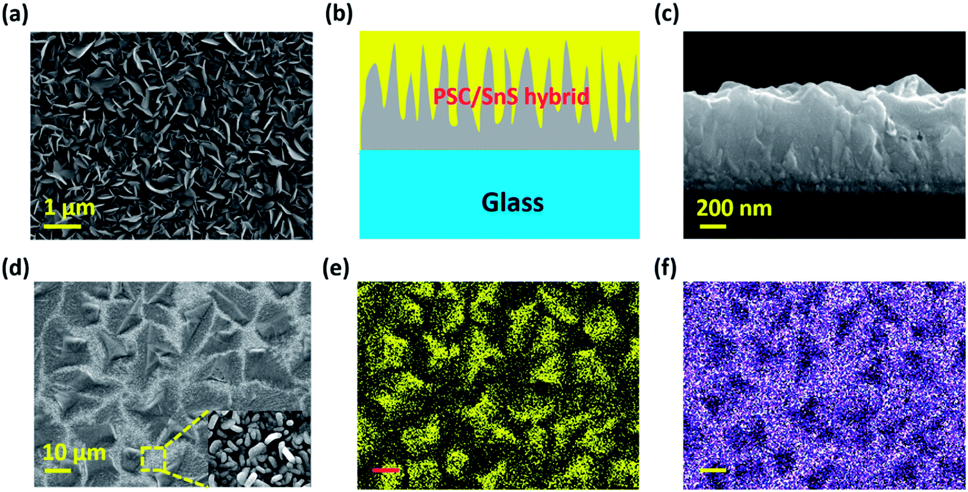 | ||
| Fig. 1 Device morphologies, schematic and elemental distribution: (a) planar-view scanning electron microscopy (SEM) image of vertically grown SnS layers, via large-area sputtering technique. (b) Schematic diagram of the hybrid CH3NH3PbI3/SnS device, (c) cross-sectional SEM of hybrid device, indicating full embedded nature of the perovskite. (d) Planar-view SEM of the CH3NH3PbI3 embedded device. The inset shows the magnified-view SEM between two grains, (e) and (f) elemental distribution of the iodine and sulphur, respectively. The scale bar for (e) and (f) are the same as (d). | ||
Apart from the material morphology, the chemical composition and crystalline structure play an important role in determining the ultimate optoelectronic performance of a device. The X-ray diffraction patterns of the as-synthesized perovskite film on glass substrate (Fig. 2a) contain intense peaks at 14.06 (110), 20.08 (112), 28.59 (220), and 40.56 (224) degrees, which matches well to the tetragonal structure for CH3NH3PbI3 (a = 8.855 Å and c = 12.659 Å).22–24 In addition, the observed sharp absorption edge at 786 nm and photoluminescence (PL) peak at 758 nm indicate the band gap of CH3NH3PbI3, closed to 1.6 eV, as presented in Fig. 2b.1,25 Further, the superior light absorption across the hybrid CH3NH3PbI3/SnS configuration relative to the pure SnS is presented in Fig. 2c. Notably, the absorption of the hybrid CH3NH3PbI3/SnS enhanced over the broad range, which can be regarded as the co-absorption of SnS and CH3NH3PbI3 films. The enhanced optical absorption facilitates us to explore it to design the advanced hybrid CH3NH3PbI3/SnS device.
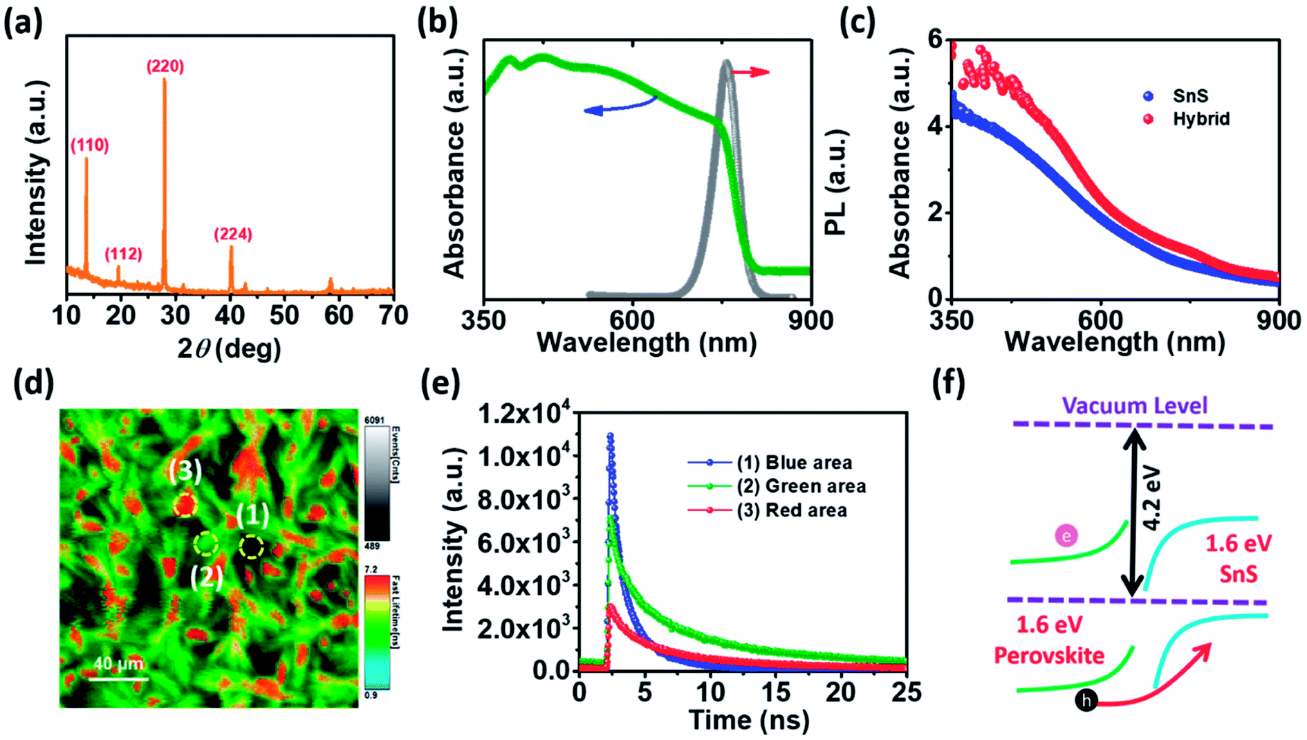 | ||
| Fig. 2 Crystal structure and optical properties. (a) XRD spectra of CH3NH3PbI3, (b) absorbance and (PL) spectra of the CH3NH3PbI3, (c) absorbance plots of the pure SnS and hybrid CH3NH3PbI3/SnS device, (d) short life decay map of the hybrid device, (e) PL decay profile from blue (1), green (2), and red (3) areas chosen from the (d). (f) Energy band diagram of the hybrid heterostructure. | ||
We therefore, sought deeper insight into the dynamics of photo-generated charge carriers in the hybrid CH3NH3PbI3/SnS device by employing time correlation single photon counting (TCSPC) technique. PL lifetimes are commonly considered as a hallmark of perovskite film quality.26 In fact, the fast PL decay is corroborated to the efficient charge transfer to the connecting layer while the slow component is associated with the carriers that do not quench well.27 To have better understanding on the charge transfer processes, we collected the spatial distribution of fast decay time of the hybrid device, as presented in the Fig. 2d. It is evident that the well grown grains exhibit a relatively slow decay time of 7.2 ns, indicating the efficient change transfer or low recombination rate to the underneath SnS.27 On the other hand, the nano size CH3NH3PbI3 on top of SnS, as observed from the magnified SEM image (inset of Fig. 1d), shows lifetime of 0.9 ns.
In addition, the PL decay profiles of from the blue (1), green (2), and red (3) areas are plotted in the Fig. 2e, with respective color lines. One can note that the peak intensity is higher for the blue plot, which can be due to the more radiative recombination from this area, indicating nanosize CH3NH3PbI3 can be utilized to design efficient PL devices. Based on literature, we draw the suitable band alignment between SnS and perovskite [Fig. 2f].19 The photo-generated holes within the CH3NH3PbI3 are transferred to the SnS due to type-II heterojunction, resulting in the improved overall performances.
To reveal the photo-generated charge generation and their collection, three different lateral (horizontal) devices e.g. pure SnS [Fig. 3a], CH3NH3PbI3 [Fig. 3b], and hybrid CH3NH3PbI3/SnS [Fig. 3c] devices were fabricated and tested under the identical conditions. Fig. 3d, e and f show the I–V curves measured for respective devices under dark and with UV illumination (λ = 365 nm, 4 mW cm−2). All curves demonstrated symmetrical and linear characteristics, confirming good ohmic contact between the ITO electrodes to SnS, CH3NH3PbI3 and hybrid devices. In addition, one can note that the hybrid device shows relatively improved photocurrent. The sequential transient photoresponse of all three devices was measured at 5 V under pulsed illumination (4 mW cm−2, λ = 365 nm) and presented in Fig. 3g, h and i. The SnS-only device shows poor photoresponse and generates only slight photocurrent (Iph = Ion − Ioff) of 0.05 μA. On the other hand, no significant response is observed for the pure CH3NH3PbI3-based device, most likely due to the charge trapping at the grain boundaries and a wide channel width (6 mm). A continuous light can generate sufficient photo carriers and change the I–V characteristics with the illumination, as shown in Fig. 3e. However, this device does not show any fast responses. On the other hand, as expected from the TCSPC measurements, the CH3NH3PbI3/SnS hybrid device shows the sufficient photocurrent of 7.1 μA. In fact, the carriers are generated across the device and move across the wide channel efficiently.
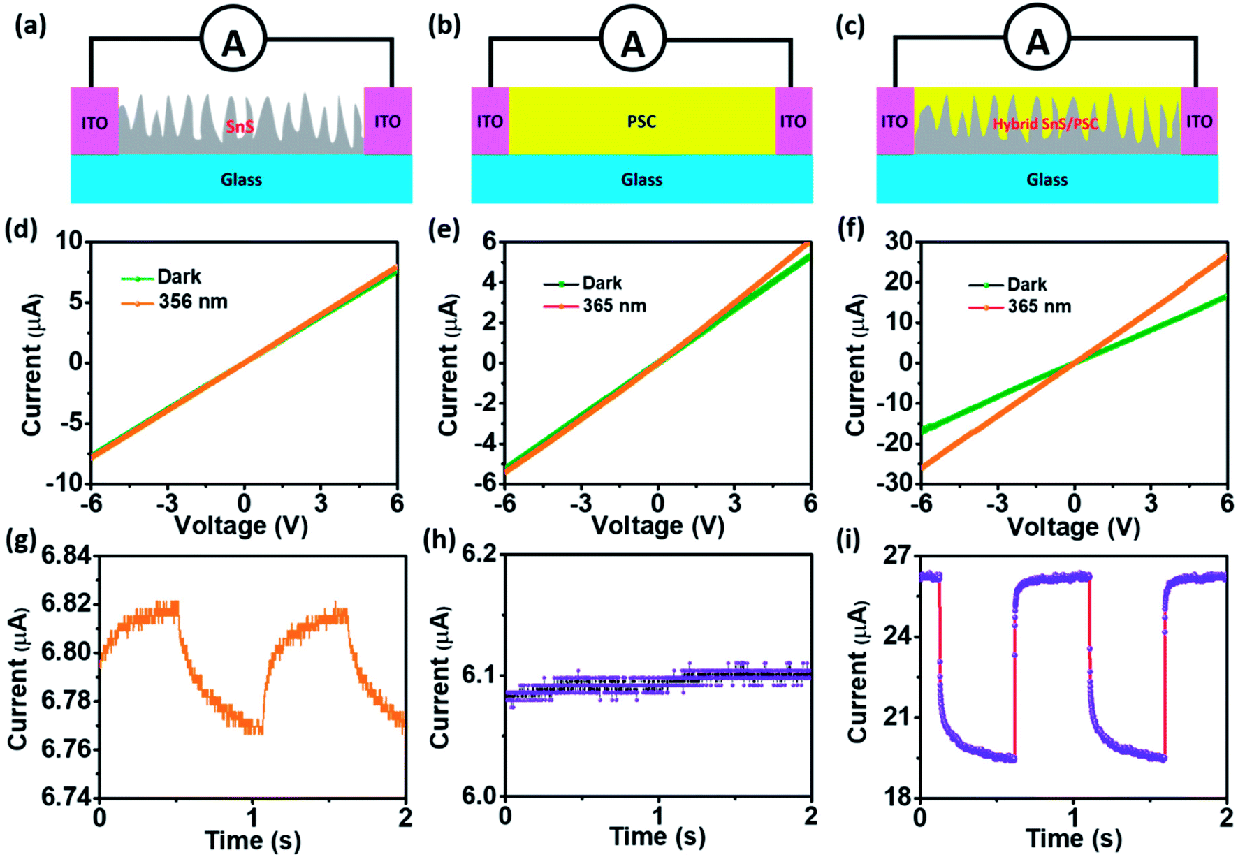 | ||
| Fig. 3 Charge transport properties: (a), (b), and (c) schematics of the lateral (horizontally) grown devices made by pure SnS, CH3NH3PbI3 and hybrid CH3NH3PbI3/SnS. (d), (e) and (f) are the corresponding current–voltage characteristics under dark and with UV (365, 4 mW cm−2) illumination. (g–i) Transient responses of the devices to 365 nm with 4 mW cm−2 illumination under 5 V bias. | ||
The temporal response is also used to calculate the rise (τrise) and decay (τdecay) times, which is closely related to the charge trapping/detrapping and recombination processes. It can be found from Fig. 4a that the rise and decay times were 9 ms and 84 ms, respectively, which is shortened compare to τrise ≈ 184 ms of the only SnS device. The response time of the hybrid CH3NH3PbI3/SnS photodetector is approximately 20 times faster than that of the only SnS-based photodetector. Further, the device exhibits reproducible response, even after 2 weeks, indicating the good stability to apply it for practical application without any capping structure. Importantly, to the best of our knowledge, the rise and fall times of the hybrid device are much faster than those of graphene or other 2D-based hybrid perovskite photodetectors, even with large channel length.12–14,18,23,28,29 Moreover, the hybrid CH3NH3PbI3/SnS photodetector was fabricated to have a wide channel length for practical applications. The cutoff frequency (f3dB) of 3 dB can also be extracted by the following equation: f3dB = 0.35/trise,1,30 and the 3 dB cutoff of the device is estimated to be 388 Hz. The role of incoming UV light intensity of the photocurrent generation is also studied and presented in Fig. 4b. The photocurrent is shown in Fig. 4c, measured at 5 V as a function of incidence intensity. It is worthy to note that the photocurrent increases sub-linearly with increasing the light intensity. The observed behavior can be fitted by a power low e.g. Iph ≈ Pn,29 where P indicates the incidence light intensity and n represents the index of the power law. The ideal value of n is 1, while n < 1 is attributed to the presence of trap states.29 For our hybrid device, the best fitted value of n is 0.76. This indicates that the trap states at the interface of perovskite and SnS can lead to recombination of photoexcited carriers. We further checked the responsivity (R) of the photodetector, which is defined as IPh/AP, where P is the illuminated intensity and A is the effective area (6 × 6 mm2).18 Initially, the R increases linearly with increasing light intensity and reaches to a peak value of ≈ 5.62 mA W−1 at 1.48 mW cm−2. The linear variation of R with low intensities is still under investigation, which needs further experimentation such as intensity-dependent PL measurements.15 On the other hand, the decrease in the R for >1.48 mW cm−2 indicates how efficiently the detector responds to an optical signal. On the other hand, the maximum value of the detectivity, which is defined as 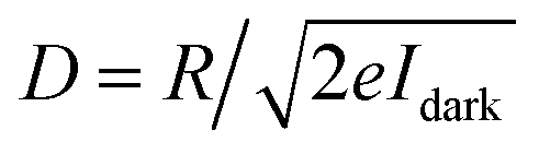 is found to be ∼2.7 × 10⁹ Jones and has the similar trends as of R.31,32
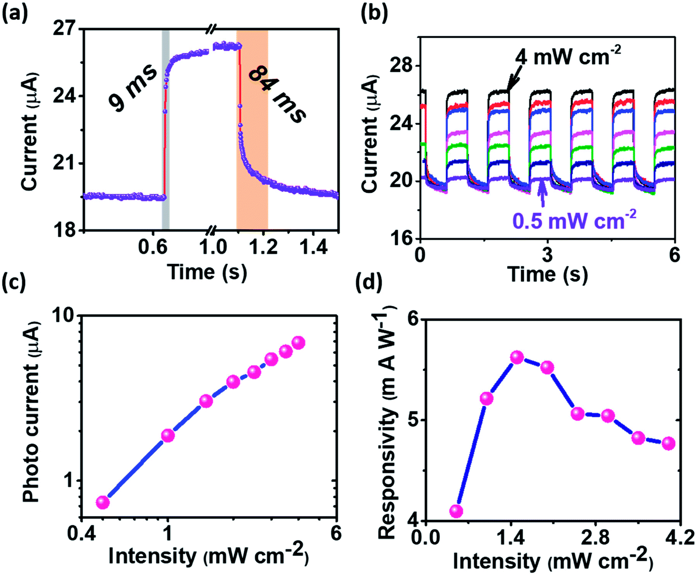 | ||
| Fig. 4 (a) Current–time characteristics of the CH3NH3PbI3/SnS device at 365 nm, 4 mW cm−2 illumination, (b) intensity-dependent response profiles of the same, (c) change in the photocurrent as a function of incoming light intensity. (d) Responsivity as a function of light illumination. | ||
Device channel width is another factor, which effectively can play an important role in the performance. Therefore, devices with different channel widths were prepared and studied. Fig. S2a† shows the dark I–V characteristics for various channel widths, varying from 6 to 10.4 mm. One can note that by increasing the channel width the resistance increases, probably due to increases in the numbers of charge trapped states. In addition, the photocurrent decreases continuously by increasing the channel width, confirming the charge trapping over wider [Fig. S2b†].
The broad band photo responsive nature of the hybrid device was tested and response for λ = 660 nm and 850 nm are depicted in Fig. 5a and b, respectively. In addition, the generation of photocurrent from 365 to 850 nm ensured the broadband spectral response from the device [Fig. 5c]. The spectral dependence of photocurrent follows the trend of the absorbance of the hybrid device [Fig. 2c]. One can see that the photocurrent decreases from UV to visible range and responds even at 850 nm.19 However, it has been predicted from the density functional theory that the band gap of the hybrid CH3NH3PbI3/SnS is reduced to NIR range, which in turn make it very suitable to design broadband photodetector. The present device may offer the possibility to design an advanced broad band photodetector over a large area.
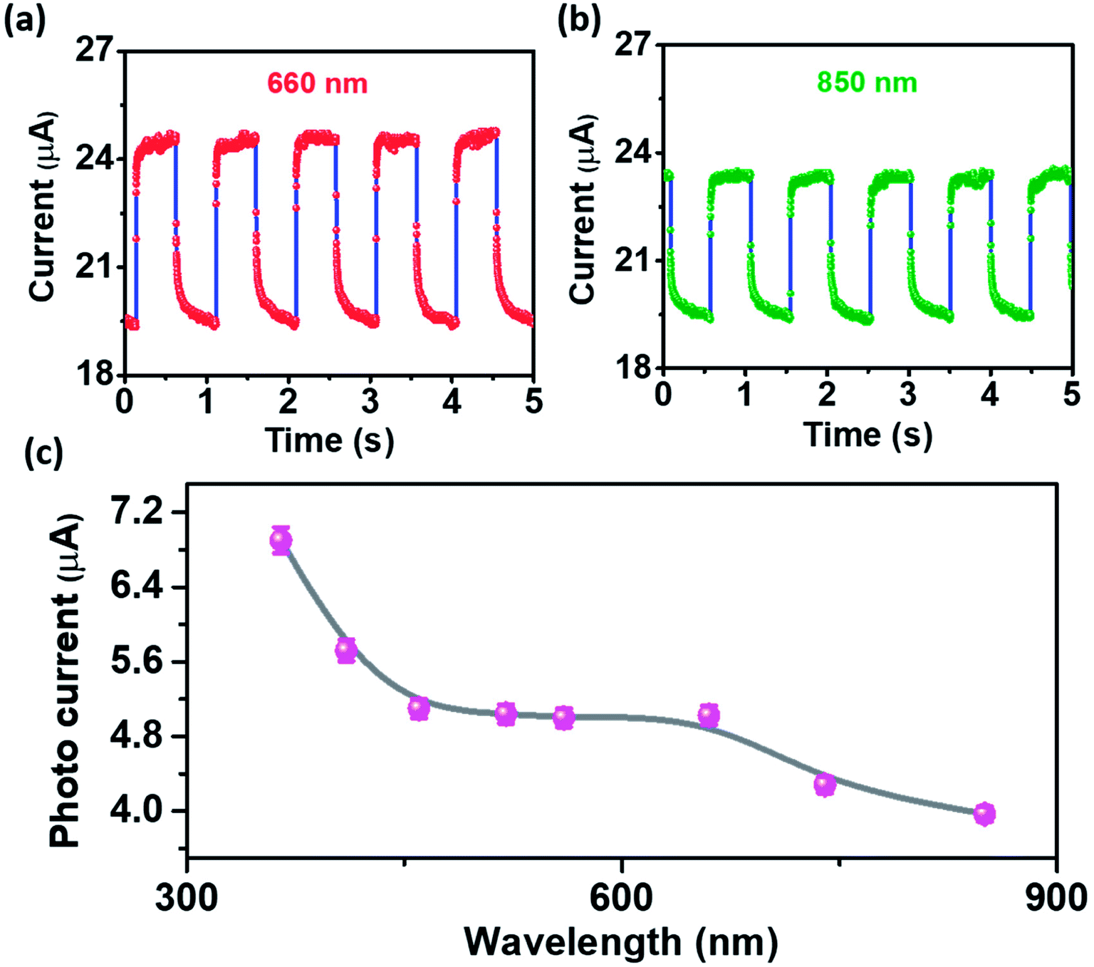 | ||
| Fig. 5 Photoresponse and broadband behavior. Transient photoresponse of the hybrid device for (a) 660 and (b) 850 nm illumination with an intensity of 4 mW cm−2 measured at 5 V. (c) Broadband distribution of the photoinduced current of the device hybrid device. | ||
4. Conclusion
In conclusion, we have demonstrated a perovskite and SnS based hybrid device. Growth of the device was confirmed by employing various techniques such as SEM, XRD, PL, and absorbance spectroscopy. The TCSPC confirmed the charge transfer professes. It has been demonstrated that the present hybrid device can be used for broadband photodetection with 20 times faster response and 140 times enhanced photocurrent value for large area applications. Finally, the broadband nature of the hybrid device, beyond the band gap of pure CH3NH3PbI3 or SnS is prediction, which matched well with the density functional theory. The resented results will open a new avenue to design a large area broadband and efficient photodetector for future advanced applications.Conflicts of interest
There are no conflicts to declare.Acknowledgements
The authors acknowledge the financial support the Basic Science Research Program through the National Research Foundation (NRF) of Korea by the Ministry of Education (NRF-2018R1D1A1B07049871 and NRF-2018R1D1A1B07045336). M. S. J. acknowledges support from the National Research Foundation of Korea (NRF) grant funded by the Korea government (MSIP) (2016R1A2B2015581). M. Kumar, H. S. Kim and D. Y. Park equally contributed to this work.References
- J. Zhou and J. Huang, Adv. Sci., 2017, 5, 1700256 CrossRef PubMed.
- L. Dou, Y. (Micheal) Yang, J. You, Z. Hong, W.-H. Chang, G. Li and Y. Yang, Nat. Commun., 2014, 5, 5404 CrossRef PubMed.
- Y. Guo, C. Liu, H. Tanaka and E. Nakamura, J. Phys. Chem. Lett., 2015, 6, 535–539 CrossRef PubMed.
- H. Deng, X. Yang, D. Dong, B. Li, D. Yang, S. Yuan, K. Qiao, Y. B. Cheng, J. Tang and H. Song, Nano Lett., 2015, 15, 7963–7969 CrossRef PubMed.
- Y.-H. Lin, P. Pattanasattayavong and T. D. Anthopoulos, Adv. Mater., 2017, 13, 1702838 CrossRef PubMed.
- C. C. Stoumpos and M. G. Kanatzidis, Adv. Mater., 2016, 28, 5778–5793 CrossRef PubMed.
- B. Yin, H. Zhang, Y. Qiu, Y. Luo, Y. Zhao and L. Hu, Nano Energy, 2017, 40, 440–446 CrossRef.
- V. Adinolfi, O. Ouellette, M. I. Saidaminov, G. Walters, A. L. Abdelhady, O. M. Bakr and E. H. Sargent, Adv. Mater., 2016, 7, 7264–7268 CrossRef PubMed.
- Y. Chen, L. Li, Z. Liu, N. Zhou, Q. Chen and H. Zhou, Nano Energy, 2017, 40, 540–549 CrossRef.
- A. Gomez, S. Sanchez, M. Campoy-Quiles and A. Abate, Nano Energy, 2018, 45, 94–100 CrossRef.
- N. Liu, H. Tian, G. Schwartz, J. B. H. Tok, T. L. Ren and Z. Bao, Nano Lett., 2014, 14, 3702–3708 CrossRef PubMed.
- Y. Wang, R. Fullon, M. Acerce, C. E. Petoukhoff, J. Yang, C. Chen, S. Du, S. K. Lai, S. P. Lau, D. Voiry, D. O'Carroll, G. Gupta, A. D. Mohite, S. Zhang, H. Zhou and M. Chhowalla, Adv. Mater., 2017, 29, 1603995 CrossRef PubMed.
- C. Ma, Y. Shi, W. Hu, M. H. Chiu, Z. Liu, A. Bera, F. Li, H. Wang, L. J. Li and T. Wu, Adv. Mater., 2016, 28, 3683–3689 CrossRef PubMed.
- J. Lu, A. Carvalho, H. Liu, S. X. Lim, A. H. Castro Neto and C. H. Sow, Angew. Chem., Int. Ed., 2016, 55, 11945–11949 CrossRef PubMed.
- B. Yang, F. Zhang, J. Chen, S. Yang, X. Xia, T. Pullerits, W. Deng and K. Han, Adv. Mater., 2017, 29, 1703758 CrossRef PubMed.
- D. H. Kang, S. R. Pae, J. Shim, G. Yoo, J. Jeon, J. W. Leem, J. S. Yu, S. Lee, B. Shin and J. H. Park, Adv. Mater., 2016, 28, 7799–7806 CrossRef PubMed.
- Y. Lin, G. Lin, B. Sun and X. Guo, Adv. Funct. Mater., 2017, 14, 1705589 Search PubMed.
- X. Song, X. Liu, D. Yu, C. Huo, J. Ji, X. Li, S. Zhang, Y. Zou, G. Zhu, Y. Wang, M. Wu, A. Xie and H. Zeng, ACS Appl. Mater. Interfaces, 2018, 10, 2801 CrossRef PubMed.
- J.-C. Li, Z.-X. Wei, W.-Q. Huang, L.-L. Ma, W. Hu, P. Peng and G.-F. Huang, ChemPhysChem, 2018, 19, 291–299 CrossRef PubMed.
- M. Patel, H.-S. Kim and J. Kim, Nanoscale, 2017, 9, 15804–15812 RSC.
- M. Kumar, M. Patel, J. Kim and D. Lim, Nanoscale, 2017, 9, 19201–19208 RSC.
- K. C. Kwon, K. Hong, Q. Van Le, S. Y. Lee, J. Choi, K. B. Kim, S. Y. Kim and H. W. Jang, Adv. Funct. Mater., 2016, 26, 4213–4222 CrossRef.
- W. Wang, Y. Ma and L. Qi, Adv. Funct. Mater., 2017, 27, 1603653 CrossRef.
- H. Huang, J. Shi, L. Zhu, D. Li, Y. Luo and Q. Meng, Nano Energy, 2016, 27, 352–358 CrossRef.
- W. Hu, W. Huang, S. Yang, X. Wang, Z. Jiang, X. Zhu, H. Zhou, H. Liu, Q. Zhang, X. Zhuang, J. Yang, D. H. Kim and A. Pan, Adv. Mater., 2017, 29, 1703256 CrossRef PubMed.
- L. Vinet and A. Zhedanov, J. Phys. A: Math. Theor., 2011, 44, 85201 CrossRef.
- J. Jiménez-López, W. Cambarau, L. Cabau and E. Palomares, Sci. Rep., 2017, 7, 1–10 CrossRef PubMed.
- J. Bouclé and N. Herlin-Boime, Synth. Met., 2016, 222, 3–16 CrossRef.
- H. Lu, W. Tian, F. Cao, Y. Ma, B. Gu and L. Li, Adv. Funct. Mater., 2016, 26, 1296–1302 CrossRef.
- V. Dhyani and S. Das, Sci. Rep., 2017, 7, 44243 CrossRef PubMed.
- M. Patel, H. S. Kim, H. H. Park and J. Kim, Appl. Phys. Lett., 2016, 108, 141904 CrossRef.
- H. S. Kim, K. R. Chauhan, J. Kim and E. H. Choi, Appl. Phys. Lett., 2017, 110, 101907 CrossRef.
Footnote |
| † Electronic supplementary information (ESI) available. See DOI: 10.1039/c8ra02825g |
| This journal is © The Royal Society of Chemistry 2018 |