
 Open Access Article
 This Open Access Article is licensed under a Creative Commons Attribution-Non Commercial 3.0 Unported Licence
Nanoridge patterns on polymeric film by a photodegradation copying method for metallic nanowire networks†
Jun Wang‡
ab,
Shuye Zhang‡ a,
Zhiyuan Shi‡a,
Jinting Jiub,
Chunhui Wub,
Tohru Sugaharab,
Shijo Nagaob,
Katsuaki Suganumab and
Peng He*a
a,
Zhiyuan Shi‡a,
Jinting Jiub,
Chunhui Wub,
Tohru Sugaharab,
Shijo Nagaob,
Katsuaki Suganumab and
Peng He*a
aState Key Laboratory of Advanced Welding and Joining, Harbin Institute of Technology, Harbin 150001, China. E-mail: hithepeng@hit.edu.cn
bThe Institute of Scientific and Industrial Research, Osaka University, Ibaraki, Osaka 567-0047, Japan
First published on 5th December 2018
Abstract
Topographical patterns are widely applied in many manufacturing areas due to the unique role in modifying performance related to physical, chemical and biological fundamentals. The patterns are usually realized by buckling or wrinkling, self-assembly or epitaxy, and lithography techniques. However, the combination of satisfactory controllability, ridge robustness, cost and dimensional precision is still difficult to achieve by any of the strategies above. A novel, simple and low-cost nanopatterning technique named “photodegradation copying method” with high technological flexibility has been initially proposed in this study. As a perfect example, a nanoridge-patterned surface has been successfully realized on a polymeric film thanks to the selective photodegradation of polymer and the shielding effect of silver nanowire (AgNW) networks. Roughness, wettability and transmittance of the polymeric film became simply and effectively controllable by adjusting the photodegradation time or the size and distribution of AgNWs. In addition, the ridge-patterned film could also be employed as a substrate in transfer printing for more flexible devices. Various topographical nanopatterns are expected to be simply realized by the photocopying method, just replacing nanowires with other masks like nanodisks, nanocubes, nanotriangles, and so on. This promising photocopying technique is believed to play an important role in the development of topographical nanopatterns, and enable more intriguing applications simply, flexibly and inexpensively.
Introduction
Topographical patterns, surface structures with regularly or randomly designed size, shape and periodicity, are employed as essential structures in several applications due to their fundamental importance to materials science, physics, chemistry and biology.1–3 The properties that are susceptive to surface/interface status such as tribological properties, wetting properties and optical properties are reported to be successfully modified by topographical patterns,3–5 which are usually taken into account for applications like microfluidic devices, medical implants, pressure sensors, and so on.6–8 In previous studies, various kinds of structures have been reported to be perfectly patterned such as ridges, grooves, micropillars and pyramids.8–12 Ridge structures including parallel straight stripes, rings, herringbone and labyrinth modes are very common topographical patterns, and could be fabricated by different methods.10,11 The methods of wrinkling, folding and release of uniaxial or equi-biaxial pre-stretch are effective ridge patterning strategies based on the mechanical deformation of substrate,3,10,13 but the limited robustness and controllability of fabricated structures hinder the application of these strategies. Besides, excellent deformation modes of the substrate are necessary for the formation of ridges, thus the materials used in these strategies are also limited. Other methods like epitaxial crystallization and evaporation-induced self-assembly directly deliver target materials to substrate, enabling ridge patterning as well.11,14 However, epitaxial crystallization only occurs when the lattices of target material and substrate match; while the size and distribution of ridges are difficult to precisely control via evaporation-induced self-assembly. Lithography techniques including dip-pen nanolithography and polymer pen lithography are known as another effective method for topographical patterning,15,16 but complicated process and expensive equipment are inevitable for nanoscale or sub-microscale precise control of patterns.In this study, a cost-effective and simple nanoridge patterning method based on selective photodegradation of polymeric film, named “photocopying method”, is proposed initially. Silver nanowire networks are coated on polymeric film and applied as mask to shield ultraviolet irradiation. Ridge patterns were fabricated by perfectly photocopying the structure of nanowire networks on polymeric film as the areas without AgNWs photodegradated and sank. The size and distribution of patterned ridges can be easily controlled, and the formed ridge patterns are mechanically stable compared with the ridges patterned by wrinkling or folding. The ridge-patterned film is able to act as substrate in transfer printing, and several properties such as roughness, wettability and transmittance also become simply controllable due to the fabricated ridge patterns, implying the great potential of this method for various intriguing applications. The universality of photocopying method is also encouraging since lots of topographical patterns are expected to form simply using different masks like nanosheets,17 nanostars,18 nanocubes19 and nanorods.20
Experimental
Synthesis of silver nanowires
The employed long and short AgNWs were synthesized by one-step polyol method at 110 °C and 150 °C, respectively, as reported in our previous studies.21 The average diameter of the long nanowire was ca. 80 nm and the average length was larger than 40 μm. The average diameter of the short nanowire was ca. 70 nm and the average length was 10–20 μm. The as-synthesized AgNWs were washed in acetone and ethanol in sequence to remove the redundant capping agent on the nanowire surface. Then the AgNWs were uniformly dispersed in ethanol to prepare the ink for the next step.Ultraviolet radiation treatment
The AgNW ink was drop-coated on the polyethylene terephthalate (PET) substrate (thickness = 100 μm, Lumirror S10, Toray) and then dried in air at room temperature for 2–3 min until the solvent was evaporated. The radial distribution of nanowires was formed using a needle vertically hanging over the horizontal PET film with the needle point immersed in the spread AgNW ink. Thus the directional flow of ink around the needle point during evaporation resulted in the radial distribution of AgNWs after drying. An ultraviolet lamp (SLUV-8, AS ONE Corp.) was applied as the UV source for the irradiation treatment in the air. The wavelength of 254 nm and the frequency of 60 Hz were chosen for the experiment. The PET film were vertically illuminated with the lamp-film distance of 5 mm. The intensity was larger than 1 mW cm−2. The continuous UV irradiation lasted for more than 600 h in the air at room temperature.Characterization and measurement
The microstructure and chemical composition was investigated with scanning electron microscopy (SEM) and energy-dispersive X-ray spectroscopy (EDS) (SU8020, Hitachi High-Technologies Co., Ltd.). All the samples were coated with platinum thin layer beforehand to improve the conductivity. The atomic force microscopy (AFM) images of the samples were obtained using a nanocute scanning probe (Scanning Probe Microscopy, SII Nanotechnology, Tokyo, Japan). The parallel transmittance (Tp) of the PET film were measured using a UV-visible/near-infrared spectrophotometer (V670, JASCO Analytical Instruments Inc.). The contact angles were measured with a contact angle analyzer (Drop Master 300, Kyowa Interface Science Co., Ltd.).The bonding strength between the AgNWs patterns and the PET substrate was tested by a 3M Scotch tape. The test was carried out 10 times in succession. The pulling force of the tape was about 0.6 N each time, and the bonding strength between the AgNWs patterns and the substrate was tested by the change of the electric resistance. The 3M Scotch tape was used to peel off the nanowires after UV irradiation. The polydimethylsiloxane (PDMS, Sylgard 184, Dow Corning Corporation) was employed in the transfer printing using ridge-patterned PET film as template.
Results and discussion
Fig. 1 illustrates the mechanism for the photodegradation of PET. The photodegradation of PET including photolysis and photooxidation has been reported in the previous studies.22,23 The photolysis refers to the chain scission of long-chain organic molecules activated by the light irradiation, leading to the decrease in molecular weight and the emergence of free radicals.22,24 In the air, the free radicals interact with oxygen easily due to the generated strongly oxidizing singlet oxygen and ozone under short-wavelength UV irradiation.25 The fragmented polymer segments gradually oxidized, and the photooxidation products such as small molecules with carboxyl end groups, aldehydes, and even carbon monoxide and carbon dioxide generate in the long-term UV irradiation.22,26–28 Actually, the polymer breakdown caused by photodegradation also has been reported.29–31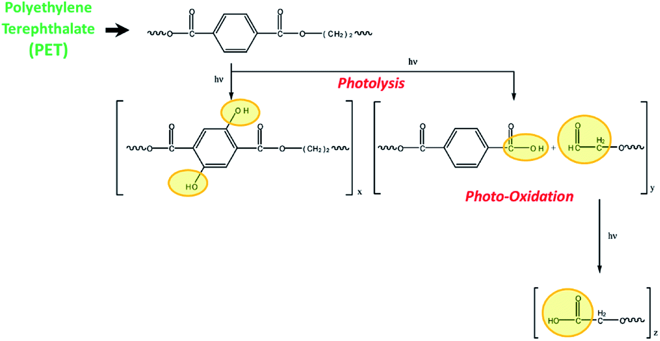 | ||
| Fig. 1 Mechanism of photodegradation of PET substrate.22 | ||
The schematic of ridge patterning process on PET film is shown in Fig. 2. As mentioned in the Experimental section, the AgNW ink was first coated on the PET film and dried for a few minutes to prepare random nanowires networks. Then the film coated with nanowires was illuminated by the UV lamp for several hours. After UV irradiation, AgNWs were completely peeled off by 3M Scotch tape due to the poor adhesion between polymeric substrate and metal nanowires. Finally, the ridges formed by copying nanowire networks were obtained. Fig. 3a and b and illustrate the SEM image of PET film coated by AgNW networks before and after the 240 h UV irradiation. Before UV irradiation, AgNWs were randomly arranged on the surface of PET film, and the film was featured by the smooth surface, while clear deformation on PET surface was observed after irradiation (Fig. 3b). The areas shielded by the nanowires were uplifted into the localize ridges as the result of deformation. In Fig. 3c, the nanowires had been peeled off by the tape and the ridges can be clearly observed. Smooth surface changed into rough one with the clear traces of AgNWs. Fig. 3d gives the tilted view of the ridges shown in Fig. 3c. The traces seem like steep ridges rose from vast plain, as the areas directly exposed to UV irradiation kept flat. To further illustrate the morphological difference between nanowires and ridges, a portion of nanowires were peeled off and other nanowires were still left on the PET film. So both the nanowires and ridges can be observed in the certain area as shown in Fig. 3e. The EDS mapping result of silver in this area is shown in Fig. 3f. It is observed that the element silver intensively distributed along the bright lines shown in Fig. 3e, indicating the bright lines were AgNWs. In comparison, silver did not intensively distributed along the dark lines in the upper half of Fig. 3e, thus these lines corresponded to the ridges on PET film. Except for the morphological difference, the nanowires and ridges also can be distinguished from AFM analysis image due to the different heights as shown in Fig. S1a.† These results suggest that the ridge patterns completely photocopied the coated AgNW networks. This can also be considered as a great example of the novel photocopying method for topographical patterns. Except for ridges, various structures can also be easily patterned just using different masks.
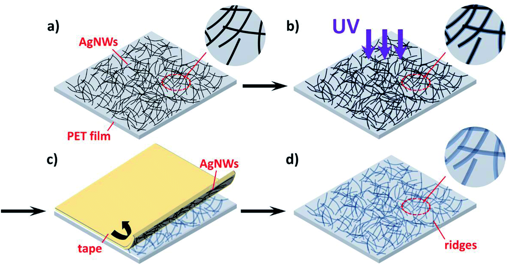 | ||
| Fig. 2 The schematic of ridge patterning process on PET film. First the AgNW ink was coated on the PET film, and the nanowires distributed randomly after drying. Then the PET film coated with AgNWs on the surface was exposed to UV irradiation, and the ridges began to emerge. After irradiation for several hours, the AgNWs were peeled off by the 3M Scotch tape. Finally, the formed ridges on the surface of PET film were confirmed. | ||
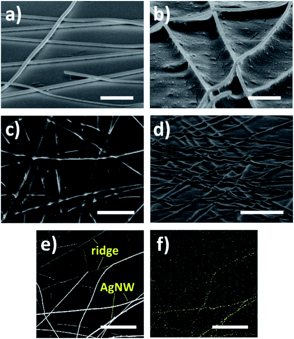 | ||
| Fig. 3 The coated AgNWs and formed ridges on the PET film. (a) The AgNWs coated on the PET film before UV irradiation (tilted view). Scale bar = 1 μm. (b) The AgNWs and emerged ridges on the PET film after UV irradiation for 240 h (tilted view). Scale bar = 1 μm. (c) and (d) The ridges on the PET film after UV irradiation, and AgNWs have been peeled off ((c) top view; (d) tilted view). Scale bar = 5 μm. (e) A part of the AgNWs have been peeled off and both the nanowires and ridges can be observed in the selected area. Scale bar = 5 μm. (f) The EDS mapping result of silver in the selected area as shown in (e). Scale bar = 5 μm. | ||
The different behaviors of the two kinds of areas on PET film, i.e. the area shielded by AgNWs and the area directly exposed to UV irradiation, imply the strong interaction between UV irradiation and the polymeric film. In the present work, the formation of ridges is closely related to the photolysis and photooxidation of PET induced by the long-term UV irradiation. Since the metal silver was not penetrated by UV light, the photodegradation did not occur at the areas shielded by AgNWs and the PET molecules in these areas were well kept after the irradiation. The photolysis and photooxidation of PET caused the sunk flat area and AgNW networks contributed to ridge networks, correspondingly forming the topographical patterns.
Fig. 4a–c demonstrates the morphology of ridges formed after UV irradiation for 6 h, 12 h and 18 h, respectively. The emerged ridges can be recognized in these three figures, but the ridges are not so obvious compared to the ones formed after 240 hour irradiation as shown in Fig. 4d. Fig. 4d illustrates the heights of ridges formed after the irradiation with different durations, and Fig. 4e–h shows the AFM images of the PET film irradiated for 6 h, 12 h, 18 h and 240 h. The height of ridge was analyzed by the AFM as well (the example was shown in Fig. S1b†). From Fig. 4d, it can be seen that the height of ridge increased if the irradiation was extended. The average height of ridge was 44.8 nm after irradiation for 6 h, and it increased to 63.5 nm after the irradiation was extended to 18 h. After 240 hour irradiation, the average height of ridge further grew to 223.1 nm. The height change also can be visually observed in Fig. 3e–h. These results indicate that the photodegradation gradually proceeded at the bared PET areas while the shielded areas kept stable in the same period, inducing the increasingly higher ridges and accordingly larger roughness of PET film after long-term irradiation. Therefore, it also indicates that it is simple and effective to control the ridge height or film roughness by adjusting the irradiation time.
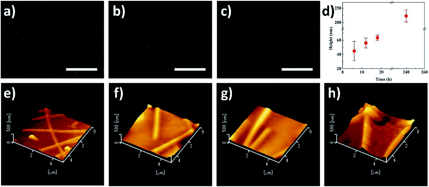 | ||
| Fig. 4 The ridges formed after UV irradiation for (a) 6 h, (b) 12 h and (c) 18 h. Scale bar = 5 μm. (d) The height of ridge formed after UV irradiation for different hours. The AFM analysis results of PET film irradiated for (e) 6 h, (f) 12 h, (g) 18 h and (h) 240 h. | ||
Except for the height of ridge, the length of ridge also can be controlled easily during the patterning—just using nanowires with different lengths as the templates. Fig. 5a and b give the ridges formed respectively using long nanowires and short nanowires as the templates. Apparently, longer ridges were obtained using long AgNWs as the template, while shorter ridges formed employing short AgNWs. Besides, it is simple to control the length of AgNWs during the synthesis using polyol method. The length of prepared nanowire correlates to the reaction parameters such as reaction temperature and stirring speed.21,32 Therefore, the length of patterned ridge on PET film can be controlled by changing the reaction parameters to prepare nanowires with different lengths as the templates. In addition to the height and length of ridge, the distribution of ridges could also be varied for different applications. Fig. 5c demonstrates the millimeter-sized square matrix formed on a large PET film by localizing the ridge networks, which was realized by peeling off the coated AgNWs with a millimeter-sized square matrix mask before UV irradiation. So in the squares there were no nanowires, and after irradiation no ridges formed in the squares correspondingly. The ridges only formed around the squares shown as the light area in Fig. 4c. Fig. 5d shows the high magnification image of the square boundary. It is observed the ridges only formed outside of the square due to the shielding effect of AgNWs and the square boundary was quite clear. Since the localizing/patterning of AgNW networks can be achieved via various printing methods,33,34 the ridge networks also can be localized or patterned easily using printed AgNW networks. On the other hand, the ridge distribution can also be regularized by nanowire alignment. The radial ridge pattern formed using radially distributed nanowires is illustrated in Fig. 5e. The AgNW networks were perfectly copied on the PET film as ridge networks, indicating multiple possibilities of ridge distributions if the nanowire alignment methods are applied.35–37 The high magnification image of the radial ridge pattern is shown in Fig. 5f. It is observed that the five radially distributed ridges were almost parallel in the selected area.
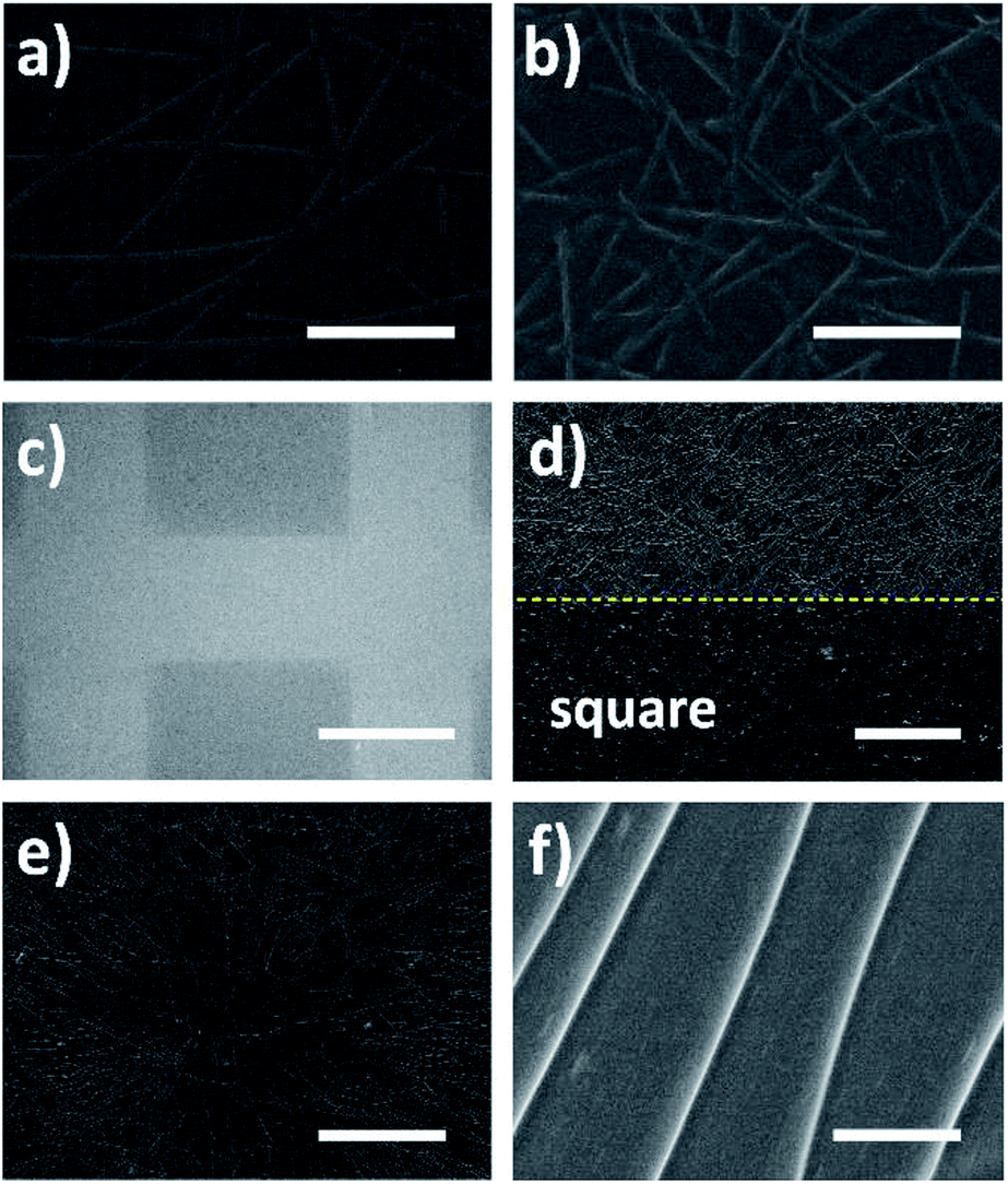 | ||
| Fig. 5 The ridges formed using (a) long nanowires and (b) short nanowires as the templates. Scale bar = 5 μm. (c) The millimeter-sized square matrix fabricated by localizing ridge distribution. Dark area (square): no ridges; light area: ridges. Scale bar = 2 mm. (d) The high magnification image of the square boundary. Scale bar = 100 μm. (e) The radial ridge pattern formed using radially distributed nanowires. Scale bar = 100 μm. (f) The high magnification image of the radial ridge pattern in (e). Scale bar = 2 μm. | ||
As mentioned above, the surface roughness increased following the formation of ridges. But except for roughness, there are also some other film properties changed due to the formation of ridges, which implies its great potential for different kinds of applications. The spread of water droplet on pristine/ridge-patterned PET films are shown in Fig. 6a and b. The contact angle on pristine PET film was 102.9°, while the contact angle on ridge-patterned PET films decreased to 38.0°. It is well known that the wettability of liquid can be adjusted by changing surface roughness.5
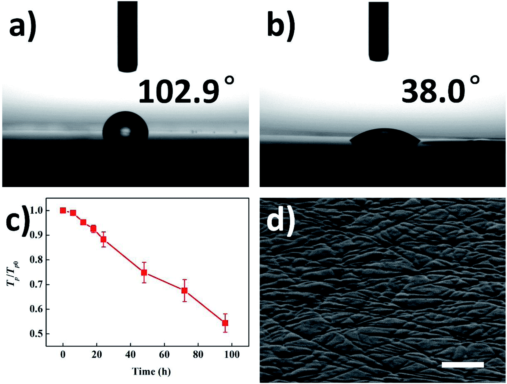 | ||
| Fig. 6 (a) and (b) The contact angle of water droplet on (a) pristine PET film and (b) ridge-patterned PET film. (c) The change of normalized parallel transmittance (Tp/Tp0, Tp: real-time parallel transmittance; Tp0: pristine parallel transmittance). (d) The grooves on the surface of PDMS film by transfer printing using the ridge-patterned PET substrate. Scale bar = 10 μm. | ||
Fig. 7 gives an ideal case of sheet resistance changing of AgNWs based transparent electrodes as a function of UV radiation time. Theoretically, when AgNWs are exposed to UV lights, sheet resistances will gradually increase by silver oxidation and sulfuration.38 According to our latest studies,39 under light irradiation, the silver migrates from internal nanowires to the surface, as a result, forming the nano-particles between nanowires. This phenomena enhances the contacts and electrical performance between AgNWs. But this lead to diameter loss in the nanowire finally, leading to the breakage at nanowires and electrical degradation. In addition, the sintering of AgNWs will improve its electrical property and joint stability, by nano-joining and surface plasmonic behaviour under UV radiation.40,41 Since the PVP is very sensitive to UV light, its mechanical properties, such as elongation at break, Young's modulus and ultimate tensile strength, are deteriorated after UV radiation, due to chemical crosslinking and chain scission changes.42
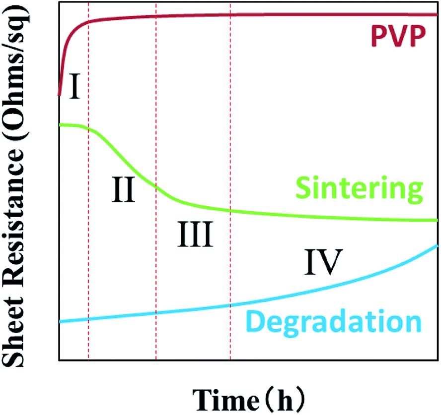 | ||
| Fig. 7 Schematic of sheet resistance changing as a function of UV irradiation time. | ||
The sheet resistance (Rs) of ridge-patterned PET film (in Fig. 6d) is measured in Fig. 8 for more than 2000 hours under UV radiation. Initially, the sheet resistance slightly increased, probably due to PVP crosslinking changes under UV lights. And then silver sintering and migration is to start, as a result, the electrical resistance of ridge-patterned PET film is gradually getting lower. The lowest point of sheet resistance of rigde-patterned PET film is found at 14.3 ohm sq−1 on the 15th day during the long term UV radiation. After that, the sheet resistances are gradually increased by the diameter loss of AgNWs. Finally, when the radiation time is over 2000 hours, the resistance becomes open.
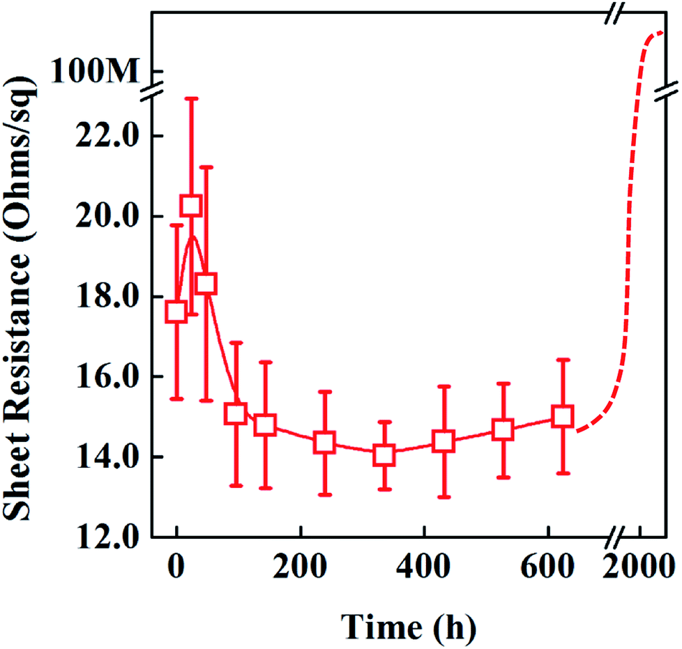 | ||
| Fig. 8 Sheet resistance (Rs) sharply increased after the UV radiation for more than 2000 hours. | ||
Fig. 9 shows the taping test results of AgNWs on the pristine and ridge-pattern PET films, respectively. As can be seen in Fig. 9, the resistance of AgNWs on the pristine PET substrate rapidly rises to above 105 times after 1 time taping test, and fails after 8 tests, indicating that the nanowires without nanojoints have poor adhesion to the substrate. The tape test greatly destroyed the conductive path in the AgNWs networks; after the UV irradiation treatment, the resistance of the initial tape test only rose to 5.17 times, and finally rose to 4669 times after the end of 10 tests, compared with the electrode without UV irradiation. As a result, the ridge-pattern PET film with AgNWs becomes much more stable than the conventional pristine PET film with AgNWs, according to these taping test results.
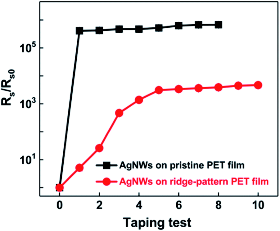 | ||
| Fig. 9 Tape test results of AgNWs on pristine and ridge-pattern PET films. | ||
Since the height, length, orientation and density of ridges are able to be controlled simply, the wettability of a certain kind of liquid on ridge-patterned film is expected to be precisely controlled. The change of normalized parallel transmittance is shown in Fig. 5c. The transmittance gradually decreased due to the intensified diffuse reflection during the generation of ridges. Similarly, the transmittance is able to be controlled simply by adjusting the size and distribution of ridges. Therefore, the controllable roughness, wettability and transmittance enable various relevant applications. The ridge-patterned PET film is also able to be used as the substrate for transfer printing. Fig. 5d gives the grooves on the surface of cured PDMS film by using the ridge-patterned PET substrate in transfer printing. Thus, the application of ridge patterning technique can be expanded to more materials by transfer printing, and the groove patterning on the surface of PDMS or other materials leads to more possible applications, such as microfluidic chips.
Conclusion
In this study, the novel and simple photocopying method for topographical nanopatterns is initially investigated. As an example, the patterning of nanoridge structures has been successfully achieved on pre-cast PET film by copying AgNW networks using UV irradiation treatment. The shielding effect of AgNWs during irradiation results in the in situ formation of ridges on PET film. The height and length of emerged ridges can be easily controlled by adjusting irradiation time and AgNW synthesis parameters. The nanoridge patterns can be localized or aligned via the alignment of AgNWs by different printing methods. Several properties such as roughness, wettability and transmittance of the PET film are modified by the generated nanoridge structure, and these properties are also controllable for various film device applications. The ridge-patterned PET film can be applied in transfer printing as substrate as well. Groove patterning is achieved by transfer printing on the surface of PDMS, enabling more possible applications and expanding the ridge patterning technique to more materials. This promising photocopying method is also capable to fabricate a series of topographical nanopatterns by replacing nanowires with other nanomaterials with different shapes. Possibly the simple, low-cost and controllable photocopying method will develop into an important technique for topographical nanopatterns and relevant applications.Conflicts of interest
There are no conflicts to declare.Acknowledgements
The authors are grateful for financial support from the National Natural Science Foundation of China (Grant No. 51805115).Notes and references
- A. Agarwal, Y. Farouz, A. P. Nesmith, L. F. Deravi, M. L. McCain and K. K. Parker, Adv. Funct. Mater., 2013, 23, 3738–3746 CrossRef CAS.
- Y. LIANG, Y. XIE, Z. ZHU, Y. JI, X. WU and Q. LIU, Nano, 2014, 09, 1450076 CrossRef CAS.
- C. Cao, H. F. Chan, J. Zang, K. W. Leong and X. Zhao, Adv. Mater., 2014, 26, 1763–1770 CrossRef CAS PubMed.
- D. Liu and D. J. Broer, Soft Matter, 2014, 10, 7952–7958 RSC.
- D. Quéré, Annu. Rev. Mater. Res., 2008, 38, 71–99 CrossRef.
- E. M. Frohlich, J. L. Alonso, J. T. Borenstein, X. Zhang, M. A. Arnaout and J. L. Charest, Lab Chip, 2013, 13, 2311–2319 RSC.
- M. Ebara, M. Akimoto, K. Uto, K. Shiba, G. Yoshikawa and T. Aoyagi, Polymer, 2014, 55, 5961–5968 CrossRef CAS.
- S. C. B. Mannsfeld, B. C. K. Tee, R. M. Stoltenberg, C. V. H. H. Chen, S. Barman, B. V. O. Muir, A. N. Sokolov, C. Reese and Z. Bao, Nat. Mater., 2010, 9, 859–864 CrossRef CAS PubMed.
- B. Su, S. Gong, Z. Ma, L. W. Yap and W. Cheng, Small, 2015, 11, 1886–1891 CrossRef CAS PubMed.
- A. Takei, L. Jin, J. W. Hutchinson and H. Fujita, Adv. Mater., 2014, 26, 4061–4067 CrossRef CAS PubMed.
- W. Sun and F. Yang, RSC Adv., 2014, 4, 45535–45539 RSC.
- F.-R. Fan, L. Lin, G. Zhu, W. Wu, R. Zhang and Z. L. Wang, Nano Lett., 2012, 12, 3109–3114 CrossRef CAS PubMed.
- H. Yabu, Y. Saito, Y. Nakamichi, Y. Hirai, S. Fujinami, K. Nakajima, T. Nishi and M. Shimomura, Polym. J., 2012, 44, 573–578 CrossRef CAS.
- Y. Kikkawa, M. Takahashi, M. Aoyagi, H. Suga, M. Kanesato and H. Abe, Macromol. Chem. Phys., 2010, 211, 2480–2483 CrossRef CAS.
- F. Huo, Z. Zheng, G. Zheng, L. R. Giam, H. Zhang and C. A. Mirkin, Science, 2008, 321, 1658–1660 CrossRef CAS PubMed.
- K. Salaita, Y. Wang and C. A. Mirkin, Nat. Nanotechnol., 2007, 2, 145–155 CrossRef CAS PubMed.
- J. Jiu, K. Suganuma and M. Nogi, J. Mater. Sci., 2011, 46, 4964–4970 CrossRef CAS.
- C. G. Khoury and T. Vo-Dinh, J. Phys. Chem. C, 2008, 112, 18849–18859 CrossRef CAS.
- D. Yu and V. W.-W. Yam, J. Am. Chem. Soc., 2004, 126, 13200–13201 CrossRef CAS PubMed.
- J. Jiu, K. Murai, D. Kim, K. Kim and K. Suganuma, Mater. Chem. Phys., 2009, 114, 333–338 CrossRef CAS.
- J. Jiu, T. Araki, J. Wang, M. Nogi, T. Sugahara, S. Nagao, H. Koga, K. Suganuma, E. Nakazawa, M. Hara, H. Uchida and K. Shinozaki, J. Mater. Chem. A, 2014, 2, 6326–6330 RSC.
- C. R. Hurley and G. J. Leggett, ACS Appl. Mater. Interfaces, 2009, 1, 1688–1697 CrossRef CAS PubMed.
- G. J. M. Fechine, R. M. Souto-Maior and M. S. Rabello, J. Appl. Polym. Sci., 2007, 104, 51–57 CrossRef CAS.
- A. I. A. Soliman, T. Ichii, T. Utsunomiya and H. Sugimura, Soft Matter, 2015, 11, 5678–5687 RSC.
- Q. Song, S. Cao, P. Zavala-Rivera, L. Ping Lu, W. Li, Y. Ji, S. A. Al-Muhtaseb, A. K. Cheetham and E. Sivaniah, Nat. Commun., 2013, 4, 1918 CrossRef PubMed.
- P. A. Christensen, T. A. Egerton, S. M. Martins-Franchetti, C. Jin and J. R. White, Polym. Degrad. Stab., 2008, 93, 305–309 CrossRef CAS.
- M. Drobota, M. Aflori, L. M. Gradinaru, A. Coroaba, M. Butnaru, S. Vlad and D. S. Vasilescu, High Perform. Polym., 2015, 27, 646–654 CrossRef CAS.
- I. Ul Ahad, A. Bartnik, H. Fiedorowicz, J. Kostecki, B. Korczyc, T. Ciach and D. Brabazon, J. Biomed. Mater. Res., Part A, 2014, 102, 3298–3310 CrossRef PubMed.
- A. Shahzad and D. H. Isaac, in Lignocellulosic Polymer Composites, John Wiley & Sons, Inc., 2014, pp. 325–367 Search PubMed.
- K. Jariashvili, B. Madhan, B. Brodsky, A. Kuchava, L. Namicheishvili and N. Metreveli, Biopolymers, 2012, 97, 189–198 CrossRef CAS PubMed.
- J. Eastoe, A. Vesperinas, A.-C. Donnewirth, P. Wyatt, I. Grillo, R. K. Heenan and S. Davis, Langmuir, 2006, 22, 851–853 CrossRef CAS PubMed.
- T. Araki, J. Jiu, M. Nogi, H. Koga, S. Nagao, T. Sugahara and K. Suganuma, Nano Res., 2014, 7, 236–245 CrossRef CAS.
- P.-H. Wang, S.-P. Chen, C.-H. Su and Y.-C. Liao, RSC Adv., 2015, 5, 98412–98418 RSC.
- B.-R. Yang, W. Cao, G.-S. Liu, H.-J. Chen, Y.-Y. Noh, T. Minari, H.-C. Hsiao, C.-Y. Lee, H.-P. D. Shieh and C. Liu, ACS Appl. Mater. Interfaces, 2015, 7, 21433–21441 CrossRef CAS PubMed.
- B. Park, I.-G. Bae and Y. H. Huh, Sci. Rep., 2016, 6, 19485 CrossRef CAS PubMed.
- S. Kang, T. Kim, S. Cho, Y. Lee, A. Choe, B. Walker, S.-J. Ko, J. Y. Kim and H. Ko, Nano Lett., 2015, 15, 7933–7942 CrossRef CAS PubMed.
- H. Lee, B. Seong, J. Kim, Y. Jang and D. Byun, Small, 2014, 10, 3918–3922 CrossRef CAS PubMed.
- R. Glover, J. Miller and J. Hutchison, ACS Nano, 2011, 5(11), 8950–8957 CrossRef CAS PubMed.
- J. Wang, J. Jiu, S. Zhang, T. Sugahara, S. Nagao, K. Suganuma and P. He, Nanotechnology, 2015, 29, 435701 CrossRef PubMed.
- S. Ding, Y. Tian, Z. Jiang and C. Wang, Mater. Trans., 2015, 56(7), 981–983 CrossRef CAS.
- P. Peng, A. Hu, A. Gerlich, G. Zou, L. Liu and Y. Zhou, ACS Appl. Mater. Interfaces, 2015, 7(23), 12597–12618 CrossRef CAS PubMed.
- A. Sionkowska, M. Wisniewski, J. Skopinska, S. Vicini and E. Marsano, Polym. Degrad. Stab., 2005, 88(2), 261–267 CrossRef CAS.
Footnotes |
| † Electronic supplementary information (ESI) available. See DOI: 10.1039/c8ra02249f |
| ‡ Dr Jun wang, Dr Shuye Zhang and Zhiyuan Shi contributed equally to this paper. |
| This journal is © The Royal Society of Chemistry 2018 |