DOI:
10.1039/C8RA01699B
(Paper)
RSC Adv., 2018,
8, 20679-20685
Essential role of enhanced surface electron–phonon interactions on the electrical transport of suspended polycrystalline gold nanofilms
Received
26th February 2018
, Accepted 27th May 2018
First published on 6th June 2018
Abstract
The electrical resistivity of suspended polycrystalline gold nanofilms with different lengths has been measured over the temperature range of 2 K to 340 K, which dramatically increases compared with bulk gold and slightly increases with length. Classical size effect theories considering surface and grain boundary scatterings cannot explain the increased film resistivity, especially the temperature dependence of resistivity, over the whole temperature range. Considering the fact that the reduction of the coordination number of atoms at the surface and the interface leads to a decrease of the phonon spectrum frequency and consequently affects the surface phonon spectrum, the electron–phonon interaction as a relatively independent surface effect is taken into account. The theoretical predictions and the experimental measured film resistivity match very well over the whole temperature range and the extracted surface Debye temperature decreases significantly compared to the bulk value, which illustrates the essential role of enhanced surface electron–phonon interactions on the electrical transport of the present gold nanofilms.
1. Introduction
Metallic nanofilms have been commonly used as interconnecting wires in modern integrated circuits (IC) and mirco/nanoelectromechanical systems (MEMS/NEMS). Study on the electrical transport of metallic thin films is of high interest to researchers and of great importance to the development of microelectronic systems.1–8 With the increase in the device density of ultra-large-scale-integrated (ULSI) and giga-scale-integrated (GSI) circuits, the characteristic scale of the interconnecting wires, taken as the thickness of nanofilms, is constantly decreasing and is comparable to the electron mean free path (MFP) of the corresponding bulk materials. As a result, the phenomenon that the electrical resistivity of thin metallic film increases dramatically with decreasing film thickness can be observed. The degraded electrical transport properties of interconnecting wires will increase the possibility of electromigration while also cause serious interconnect delay that the interconnect delay tends to dominate the logic delay, which may even cause the whole system to fail. To ensure the reliability and stability of these sophisticated IC and MEMS/NEMS, the in-depth analysis of the electrical properties of metallic nanofilms need to be carried out.5,9
To figure out the size effect, Fuchs and Sondheimer (FS),10,11 and Mayadas and Shatzkes (MS),12,13 considered that the motion of electrons is confined by the surfaces and grain boundaries and proposed the theories of surface scattering and grain boundary scattering, respectively. Later lots of experimental data was fit with the FS and the MS theories to have an in-depth analysis to the origin of the size effect and the results indicate that grain boundary scattering dominates the electrical transport of polycrystalline metallic nanofilms.14–20
Besides the FS and the MS theories, Bloch-Gruneisen21 (BG) theory was also applied to describe the size effect of temperature-dependent resistivity between experimental and bulk values. The effective Debye temperatures obtained by fitting with the BG theory show a significant reduction compared with the corresponding bulk values as width,22 thickness,23 and average particle diameter24 of nanofilms are reduced. Called phonon softening effect, this phenomenon is pointed to be related to surface bond-order loss25 and surface roughness26 of nanofilms. As for the temperature-independent part, the residual resistivity of nanofilms ρ0 (which we take as the resistivity at 4.2 K, i.e., ρ4.2 K ≈ ρ0) is equally important. Measurements have demonstrated that ρ0 increases with deceasing film width and thickness.22–24,27
It needs to be pointed out that in most of existing experiments the metallic nanofilms are deposited on the substrates, such as mica,8,28–30 SiO2/Si,31,32 SiOC,22 fused quartz33 and so on. As a result, the effects of interface contact on the measurements cannot be ignored. Meanwhile the generated Joule heat will make the average temperature along the length of nanofilm be slightly higher than the set ambient temperature when using the conventional four-wire method to measure the resistivity, which weakens the accuracy of the experimental results. The suspended structure and the direct current heating method introduced in ref. 5 and 14 can avoid the influence of interface contact and Joule effect on the measurements, respectively. However, their experimental temperatures are above 77 K (the boiling point of liquid nitrogen) due to the limitation of experimental equipment. As a result, their previous analysis has limitations.5,14,34 Hence, it is urgent to expand their experimental temperature range.
In this paper, studies on the electrical resistivity of suspended gold (Au) nanofilms with different length (L) in a temperature range of 2 K to 340 K have been carried out to figure out the contribution of different mechanisms to the resistivity of nanofilms. It should be noted that the effects of substrate and contact resistance on the measured electrical resistivity have been eliminated in view of the present special designed suspended structure.
2. Experiment
2.1 Suspended gold nanofilms preparation
The suspended gold nanofilms used in this study are fabricated by electron beam (EB) physical vapor deposition, assisted with EB lithography and the isotropic/anisotropic etching techniques. In this structure, the electrodes and nanofilm are integrally prepared, the electrodes are deposited on SiO2 and only the nanofilm is suspended. The fabrication processes in details can be referred in ref. 6 and 34. With the same thickness (d) of 49.4 nm and width (w) of 450 nm, the length of the same batch of nanofilms is 15 μm, 10 μm and 6 μm respectively. After the preparation, we conducted the scanning electron microscopy (SEM) and X-ray diffraction (XRD) experiments. Fig. 1 illustrates a fabricated sample structure. It should be noted that the actual size of electrodes is centimeter level and is far larger than the characteristic scale of nanofilms. As a result, the electrodes have no size effect. Hence the electrical resistivity of electrodes is much small than that of nanofilms and can be ignored.
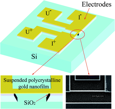 |
| | Fig. 1 Scanning electron microscopy (SEM) image of a suspended polycrystalline Au nanofilm (L = 15 μm, d = 49.4 nm and w = 450 nm) and schematic diagram of corresponding direct current heating method measurements. | |
2.2 XRD spectra of the suspended gold nanofilms
The average grain size of nanofilms can be investigated by XRD method. Fig. 2 shows the XRD spectra of the 15 μm long suspended gold nanofilm. Based on the experimental results and Scherrer equation, the average grain sizes of nanofilms are calculated as 24.7 nm.
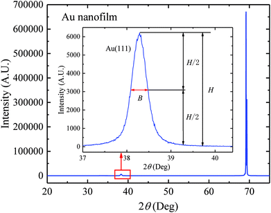 |
| | Fig. 2 X-ray diffraction spectra of the 15 μm long nanofilm. Insert: the partial enlargement of Au(111) part, B is the full-width-at-half-maximum (FWHM). | |
2.3 Resistivity measurement method
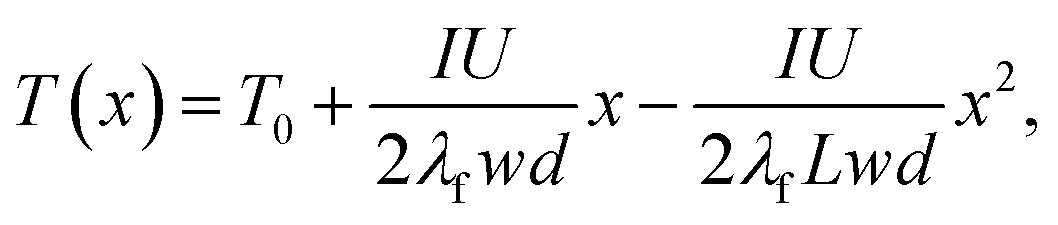
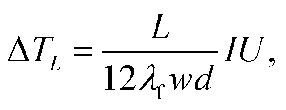
Due to the small heat capacity of suspended nanofilms, the measurements are always affected by the magnitude of heating current. A slight increment in current will induce the Joule effect which in turn results in a change in resistivity. Nevertheless, the relatively low current can lead to an inaccurate experimental result. Hence, a direct current heating method5,14 is applied to exactly extract the electrical resistivity of the nanofilms in this work. When a constant heating current is fed on the nanofilm, parabolic temperature distribution is built due to the one-dimensional steady-state heat transfer process. Treated as heat sinks, the electrodes maintain the cavity temperature T0. The temperature distribution T(x) and average temperature rise (ΔTL) along the length of film can be expressed as,| |
 | (1) |
| |
 | (2) |
where I and U are the direct current and voltage applied on the film, respectively; λf is the in-plane thermal conductivity of film. Then taking into account the current heating effect, we obtain the apparent resistivity of the film (ρa) through,| |
 | (3) |
where β = (ρf − ρref)/[ρref(T0 − Tref)] is the temperature coefficient of resistance (TCR); ρf is the intrinsic resistivity at T0; ρref is the reference resistivity at reference temperature Tref (273.2 K). As can be seen from eqn (3), the resistivity of thin film ρf at T0 can be extracted from the intercept of ρa–IU curve which is the corresponding resistivity at zero heating power.
In measurement, the silicon chip is fixed on the special designed base with acetal glue. Then we operate a bonding machine (West Bond 7476D-79) to connect the electrodes on our sample with those on the base with gold bond wires. After bonding, the base is mounted in the physical property measurement system (PPMS) in which temperature (T) can be adjusted from 1.9 K to 400 K and absolute pressure is less than 9 × 10⁻⁶ torr. The four-probe (U+, I+, I−, U− in Fig. 1) resistance measurement is performed with a high precision DC voltage source (Advantest R6243) and two high-precision digital multimeters (Keitheley 2002, 8.5 digits), in which a digital multimeter and a standard resistance (Yokogawa 2792) are used to detect the electrical current. The measurement details can be referred in ref. 5 and 14.
3. Results and discussion
3.1 Electrical properties of the suspended gold nanofilms
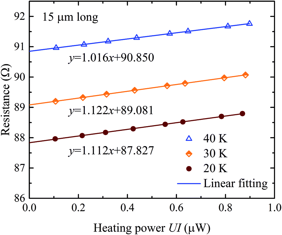
Shown in Fig. 3 as an example, the resistance of Au nanofilm increases with heating power and the ρa–IU curves of 15 μm long nanofilm at 40 K, 30 K and 20 K measured by the direct current heating method have a nice linearity. We can extract the resistance values from the intercept of linear fitting curves at 40 K, 30 K and 20 K are 90.850 Ω, 89.081 Ω and 87.827 Ω, respectively.
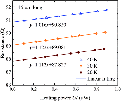 |
| | Fig. 3 The ρa–IU curves measured by the direct current heating method and the corresponding linear fitting curves of 15 μm long nanofilm at 40 K, 30 K and 20 K. | |
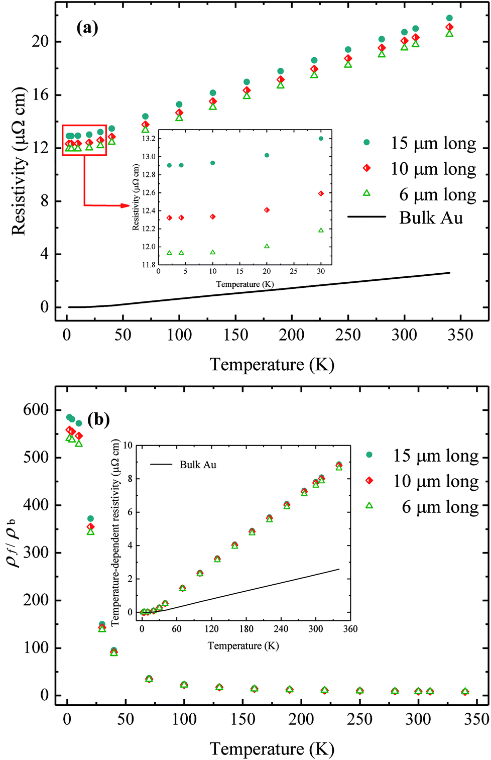
Fig. 4(a) shows the extracted resistivity of Au nanofilms with different length within a range from 2 K to 340 K. It is necessary to point out that the minimum temperature for our experiment is 2 K. Illustration in Fig. 4(a) is the partial enlargement in a temperature range of 2 K to 30 K. It can be found that ρf reaches a residual value at T = 4.2 K for all samples. Both the intrinsic resistivity and residual resistivity have significant increments compared with the corresponding bulk values and increase slightly with length. From Fig. 4(b), the resistivity ratio between the nanofilm and bulk Au dramatically increases with decreasing temperature, which is related to the increased residual resistivity and the sharp decrease of mean free path of conduction electrons. Illustrated in the inset of Fig. 4(b), the enhancement of temperature-dependent resistivity of nanofilms can also be found.
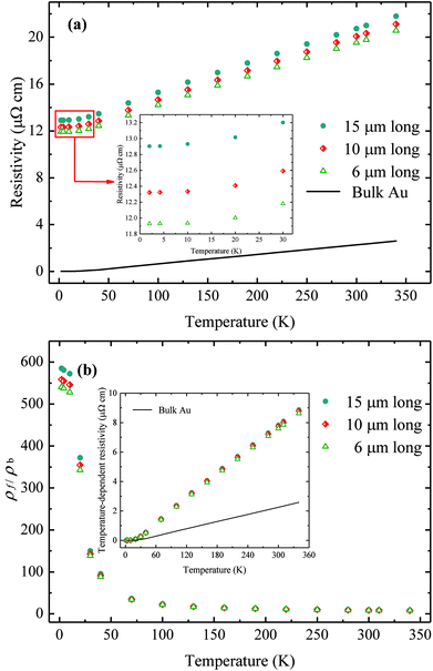 |
| | Fig. 4 (a) The extracted resistivity of Au nanofilms (L = 15 μm, 10 μm and 6 μm, d = 49.4 nm and w = 450 nm) as a function of temperature. Inset: the partial enlargement in a temperature range from 2 K to 30 K; (b) the ratio between extracted and the bulk resistivity (ρf/ρb) as a function of temperature. Inset: the measured temperature-dependent resistivity of Au nanofilms (L = 15 μm, 10 μm and 6 μm, d = 49.4 nm and w = 450 nm) as a function of temperature. | |
3.2 Role of the grain boundary and surface scatterings
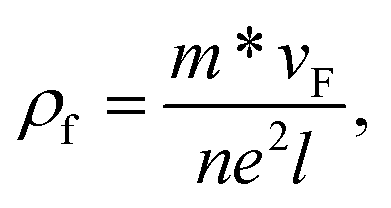
The resistivity of the complex nanostructure can be well described by the Landau-Fermi liquid theory:35,36| |
 | (4) |
where m* is the effective carrier mass, vF is the Fermi velocity, n is the carrier concentration, e is the elementary charge and l is the mean free path of conduction electrons. l in the eqn (4) is related to various scattering mechanisms. The product ρfl = 0.96 fΩ m2 for bulk pure Au can be used as the reference.36 Based on the extracted ρf, we calculated the l of the suspended nanofilms. Shown in the Fig. 5, the mean free path l for suspended nanofilms increases with decreasing temperature and is much less than the corresponding bulk values, especially at low temperatures. Need to point out once again that our minimum experimental temperature is 2 K. It is also clear that the l of nanofilms is less than the nanofilm thickness and mean grain size, which indicates that grain boundary and surface are indeed weakening the electrical transport properties of nanofilms.
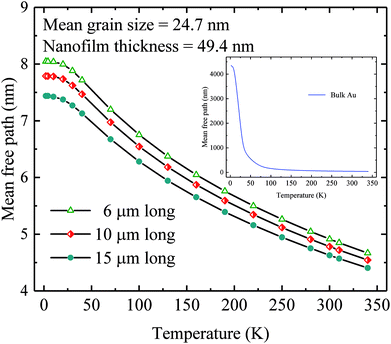 |
| | Fig. 5 The calculated electron mean free path of nanofilms with different length in a temperature range from 2 K to 340 K based Landau-Fermi liquid theory. Inset: the calculated electron mean free path of bulk Au. | |
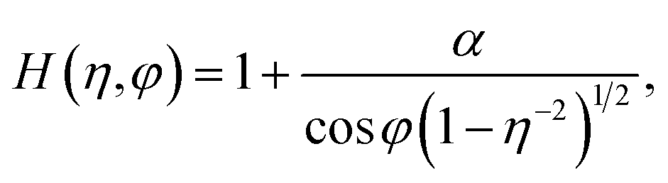
According to Matthiessen's rule, the resistivity of nanofilm basically consists of surface and grain boundary scatterings, defect, and impurity scattering.22 Defects and impurities are known to accumulate in grain boundaries owing to a purification of the grains during grain growth. Further, they both reduce the effective MFP of conduction electrons and have the same effects with grain boundary scattering on the temperature dependence of resistivity.37 Hence, defect and impurity scatterings are included in grain boundary scattering. The grain boundary reflection coefficient (Rg) and the specular reflection coefficient (p) are the important parameters in the MS and the FS theories respectively. Rg describes the fraction of electrons reflected from grain boundary and p describes the probability for an electron to be specularly reflected from the film surface. Both Rg and p range from 0 to 1, and when Rg = 0 or p = 1, the effects of grain boundary scattering and surface scattering are neglected, respectively. For Au nanofilms, the specular reflection coefficient p is usually taken to be 0.5.38 The combined influences of grain boundary and surface on the resistivity can be expressed as,
| |
 | (5) |
H(
η,
φ) is given by,
| |
 | (6) |
where
ρMS+FS is the predicted resistivity of the combined MS–FS theory;
ρb represents bulk Au electrical resistivity;
α =
lbRg/[
D(1 −
Rg)],
lb is the bulk electron MFP calculated by Drude's relation (
lb = 40.8 nm at 273.2 K) and
D = 24.7 nm is the mean grain size investigated by XRD;
ξ =
d/
lb.
Since the 10 μm and 6 μm long nanofilms are similar to the 15 μm long film, the fitting curves of only 15 μm long nanofilm are plotted in Fig. 6 as an example. In order to compare the contribution of grain boundary scattering and surface scattering to the increased resistivity, the curves of only considering MS and FS are also given in Fig. 6. Even when p = 0 in the FS theory, which means a completely diffusive scattering at the surface and corresponds to a maximum resistivity, the predicted resistivity is only increased slightly compared with the bulk value and much smaller than the measured resistivity. It indicates that grain boundary scattering is the dominant determinant of intrinsic resistivity and residual resistivity in the present films. However, surface scattering cannot be ignored due to a visible increment for the MS–FS curve compared with the MS curve. The extracted Rg for 6 μm, 10 μm and 15 μm long nanofilms is 0.721, 0.728 and 0.737 respectively, and agrees well with ref. 14 in which Rg is 0.7. It is also found that Rg increases slightly with length, which indicates that grain boundary scattering is enhanced. The observed predominant grain boundary scattering may include scattering from impurities at the grain boundaries,37,39 which can be corroborated by the reduction of residual resistivity ratio (RRR) listed in Table 1. As a rough index of the purity of a sample, RRR decreases with increasing defects, and the RRR of bulk Au is 102. Nevertheless there is still a significant deviation in the temperature dependent part between MS–FS theory predictions and experimental results.
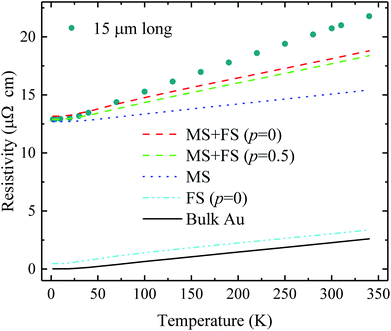 |
| | Fig. 6 Experimental results from 2 K to 340 K and the corresponding MS–FS theory fitting curves of the 15 μm long nanofilm. | |
Table 1 The electrical properties and fitting parameters of the nanofilms. It should be noted that Rg and p in the combined MS–FS theory are the same with these of the combined MS–FS–SEPI theory
| L (μm) |
ρf (μΩ cm) |
RRR |
MS + FS + BG |
MS + FS + SEPI |
| 4.2 K |
300 K |
ρ300 K/ρ4.2 K |
Rg |
p |
KD (μΩ cm) |
ΘD (K) |
Rg |
p |
KS (μΩ cm) |
ΘS (K) |
| 6 |
11.93 |
19.53 |
1.637 |
0.51 |
0.5 |
5.08 |
83 |
0.721 |
0.5 |
5 |
131 |
| 10 |
12.32 |
20.07 |
1.629 |
0.52 |
0.5 |
5.08 |
83 |
0.728 |
0.5 |
5.08 |
127 |
| 15 |
12.91 |
20.73 |
1.607 |
0.54 |
0.5 |
5.08 |
83 |
0.737 |
0.5 |
5.12 |
125.3 |
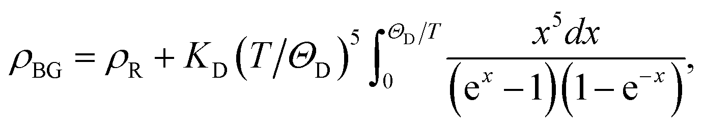
3.3 Role of electron–phonon interaction
To explore the underlying mechanism responsible for the discrepancy, we take electron–phonon interaction into account. Electron–phonon interaction is used to analyze the resistivity temperature dependence and can be accounted by BG theory which is in the framework of the Boltzmann transport theory. It should be noted that electron–phonon interaction is similar to grain boundary scattering and surface scattering, that is, all of them will affect the temperature dependence of the resistivity of thin film. With the decrease of film thickness and grain size, the atomic fraction of the surface and the interface increases significantly, and the reduction of the coordination number of atoms at the surface and the interface leads to a decrease of the phonon spectrum frequency, which affects the surface phonon spectrum and Debye temperature of the film.22–24,31 Since the spectrum of the surface phonons is softened, compared with the bulk behavior, many studies take the electron–phonon interaction as a bulk effect and name it phonon softening effect.34,40 As a result, bulk Au resistivity is increased and the modified bulk resistivity (ρBG) can be obtained by the BG theory as expressed by,21| |
 | (7) |
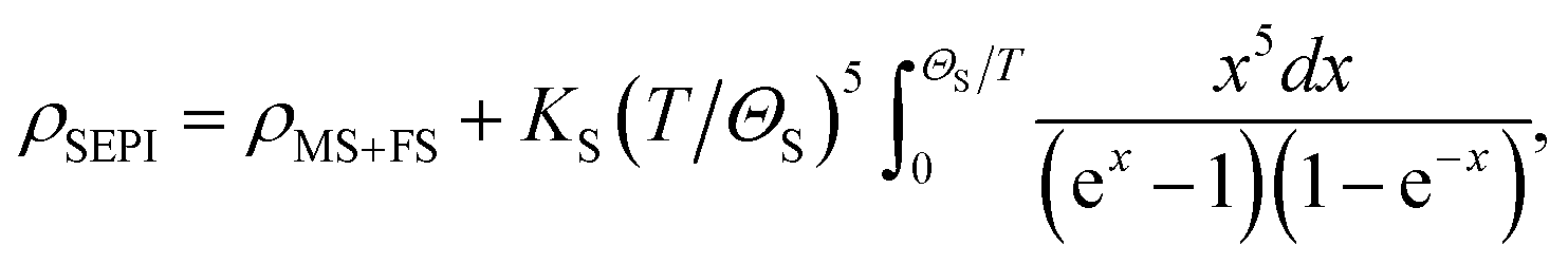
where ρR = 0.022 μΩ cm is the residual resistivity in bulk Au; KD is the prefactor; ΘD is Debye temperature. Then combining the effects of FS and MS, one can replace ρb in eqn (5) with ρBG and fit experimental data to this combined MS–FS–BG theory.34 However, since the effect of surface phonon spectrum on the thin film is not equivalent to the BG bulk, the surface electron–phonon interaction should be regarded as a relatively independent surface effect and not a bulk effect. Taken as an enhancement of surface electron–phonon interaction (SEPI),31 the contribution of electron–phonon interaction to the electrical resistivity can be superimposed on that of grain boundary scattering and surface scattering. It complies well with the fact that phonons are frozen out at 4.2 K,28 hence the effect of electron–phonon interaction on the electrical transport properties of metallic thin films can be ignored below 4.2 K. Comprehensively considering the effects of SEPI, grain boundary and surface scatterings, we obtain the predicted resistivity ρSEPI with the following equation,| |
 | (8) |
where ρMS+FS is given by eqn (5); KS is the prefactor; ΘS is the surface Debye temperature.
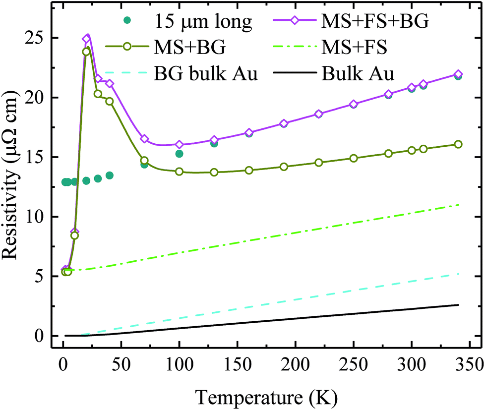
For the combined MS–FS–BG theory, the fitting curves of 15 μm long nanofilm are shown in Fig. 7. It is found that the fitting curve can agree with experimental results above 130 K and shows an unacceptable fluctuation below 130 K, which indicates the inapplicability of this combined MS–FS–BG theory.
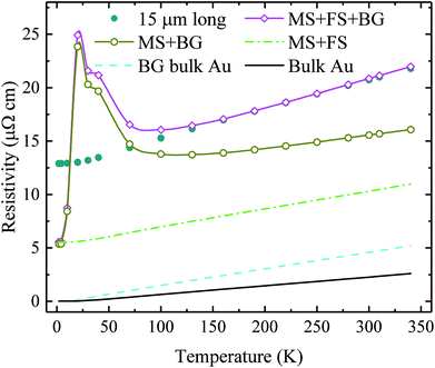 |
| | Fig. 7 Experimental results from 2 K to 340 K and the corresponding and the combined MS–FS–BG theory fitting curves of the 15 μm long nanofilm. | |
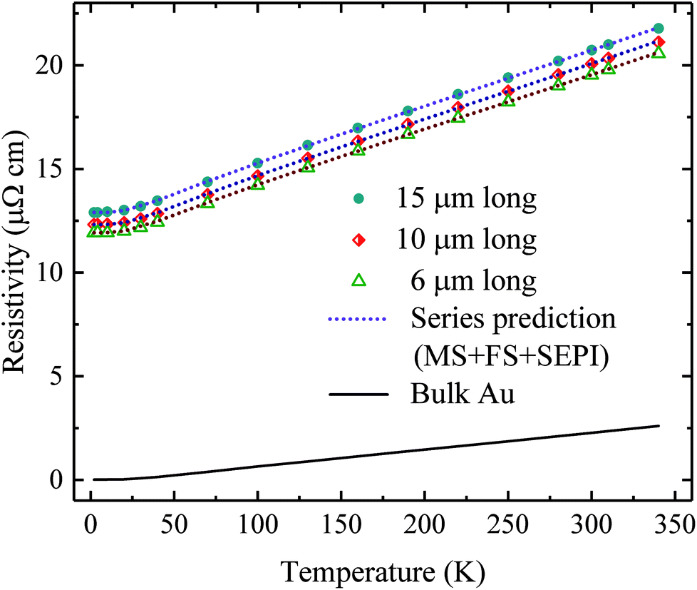
For the combined MS–FS–SEPI theory, the fitting curves are given in Fig. 8. It is found that the combined MS–FS–SEPI theory follows the experimental results quite well in whole temperature range, which verifies the reliability of this model. It should also be pointed out that the fitting results are in line with fact that phonons are frozen out at 4.2 K which means the contribution of surface electron–phonon interaction to the resistivity below 4.2 K is small enough to be neglected. Based on the comparison of the fitting curves of MS–FS–SEPI theory and MS–FS–BG theory, it is evident that the effect of surface phonon spectrum on the thin film is more closely linked to surface and cannot be equivalent to the BG bulk. This indicates that it is more reasonable to take electron–phonon interaction as a relatively independent surface effect. The fitting parameters are given in Table 1. It should be noted that Rg and p in the combined MS–FS theory are the same with these of the combined MS–FS–SEPI theory. We attribute the variation in Rg along length of the present nanofilms to the grain boundary scattering which may include scattering from impurities at the grain boundaries. The extracted surface Debye temperature for 6 μm, 10 μm and 15 μm long nanofilms is 131 K, 127 K and 125.3 K respectively and shows a sharp decline compared with bulk Au value 170 K, which indicates an enhancement of temperature dependence of resistivity. It is also found that the prefactor increases and the surface Debye temperature decreases with increasing length, which illustrates the enhancement of surface electron–phonon interaction increases with length.
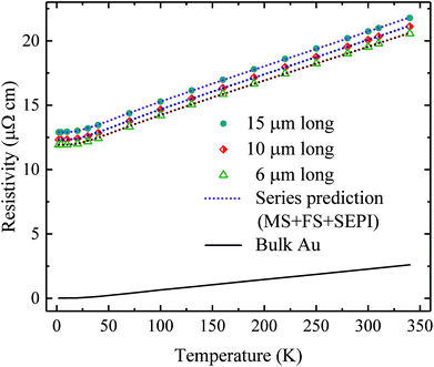 |
| | Fig. 8 Experimental results from 2 K to 340 K and the corresponding combined MS–FS–SEPI theory fitting curves. | |
4. Conclusion
Without the influence of substrate, contact resistance and Joule heat effect, the electrical resistivity of three suspended polycrystalline gold nanofilms with different length has been measured. The measured electrical resistivity increases greatly compared to the bulk value. Applying the classical size effect theories considering surface and grain boundary scatterings, we find that the grain boundary scattering dominates the electrical conduction and the extracted grain boundary reflection coefficient is about 0.73 for the present nanofilms. However, there is a discrepancy between experimental and theoretical values in temperature-dependent resistivity. The theory that takes electron–phonon interaction as a bulk effect is invalid below 130 K. We take the electron–phonon interaction as an enhancement of surface electron–phonon interaction into account. The experimental results can be described very well in the whole temperature range, which demonstrates that the effect of surface phonon spectrum on the thin film is more closely linked to surface. The extracted surface Debye temperatures decrease from the bulk value of 170 K to between 131 K and 125.3 K and tend to decrease slightly with increasing film length. The results illustrate the essential role of enhanced surface electron–phonon interaction on electrical transport of the present suspended polycrystalline gold nanofilms.
Conflicts of interest
There are no conflicts to declare.
Acknowledgements
This work was supported by the National Natural Science Foundation of China (Grant No. 51776224, 51576105, 51636002, 61701470, and 51336009), the Science Fund for Creative Research Groups (Grant No. 51621062), and the Tsinghua University Initiative Scientific Research Program.
Notes and references
- H. G. Craighead, Science, 2000, 290, 1532 CrossRef PubMed.
- M. Imboden and P. Mohanty, Phys. Rep., 2014, 534, 89–146 CrossRef.
- M. César, D. Liu, D. Gall and H. Guo, Phys. Rev. Appl., 2014, 2, 044007 CrossRef.
- X. Liang and L. Shen, Acta Mater., 2018, 148, 100–109 CrossRef.
- W. G. Ma and X. Zhang, Int. J. Heat Mass Transfer, 2013, 58, 639–651 CrossRef.
- K. Nishimura, H. D. Wang, T. Fukunaga, K. Kurata and H. Takamatsu, Int. J. Heat Mass Transfer, 2016, 95, 727–734 CrossRef.
- F. Misjak, K. H. Nagy, P. Lobotka and G. Radnoczi, J. Appl. Phys., 2014, 116, 083507 CrossRef.
- R. C. Munoz and C. Arenas, Appl. Phys. Rev., 2017, 4, 011102 Search PubMed.
- N. Srivastava and K. Banerjee, JOM, 2004, 56, 30–31 CrossRef.
- K. Fuchs, Math. Proc. Cambridge Philos. Soc., 1938, 34, 100–108 CrossRef.
- E. H. Sondheimer, Advances in Physics, 1952, 1, 1 CrossRef.
- A. F. Mayadas, M. Shatzkes and J. F. Janak, Appl. Phys. Lett., 1969, 14, 345–347 CrossRef.
- A. F. Mayadas and M. Shatzkes, Phys. Rev. B: Solid State, 1970, 1, 1382–1389 CrossRef.
- Q. G. Zhang, B. Y. Cao, X. Zhang, M. Fujii and K. Takahashi, Phys. Rev. B: Condens. Matter Mater. Phys., 2006, 74, 134109 CrossRef.
- C. Charpentier, P. Prodhomme and P. R. I. Cabarrocas, Thin Solid Films, 2013, 531, 424–429 CrossRef.
- J. M. Rickman and K. Barmak, J. Appl. Phys., 2013, 114, 133703 CrossRef.
- D. Choi, X. Liu, P. K. Schelling, K. R. Coffey and K. Barmak, J. Appl. Phys., 2014, 115, 104308 CrossRef.
- K. Moors, B. Soree, Z. Tőkei and W. Magnus, J. Appl. Phys., 2014, 116, 063714 CrossRef.
- X. Cao, Y. Yamaguchi, Y. Ninomiya and N. Yamada, J. Appl. Phys., 2016, 119, 025104 CrossRef.
- S. S. Yeh, W. Y. Chang and J. J. Lin, Sci. Adv., 2017, 3, e1700135 CrossRef PubMed.
- J. M. Ziman, Electrons and Phonons: the Theory of Transport Phenomena in Solids, Clarendon Press, 1960 Search PubMed.
- W. Zhang, S. H. Brongersma, Z. Li, D. Li, O. Richard and K. Maex, J. Appl. Phys., 2007, 101, 063703 CrossRef.
- A. Bid, A. Bora and A. K. Raychaudhuri, Phys. Rev. B: Condens. Matter Mater. Phys., 2006, 74, 035426 CrossRef.
- B. Roy and D. Chakravorty, J. Phys.: Condens. Matter, 1990, 2, 9323 CrossRef.
- T. C. A. Yeung, T. C. Chiam, C. K. Chen, C. Q. Sun, W. Z. Shangguan, W. K. Wong and C. H. Kam, Phys. Rev. B: Condens. Matter Mater. Phys., 2005, 72, 155417 CrossRef.
- Y. P. Timalsina, A. Horning, R. F. Spivey, K. M. Lewis, T. S. Kuan, G. C. Wang and T. M. Lu, Nanotechnology, 2015, 26, 075704 CrossRef PubMed.
- G. Kästle, H. G. Boyen, A. Schröder, A. Plettl and P. Ziemann, Phys. Rev. B: Condens. Matter Mater. Phys., 2004, 70, 155109 CrossRef.
- R. C. Munoz, J. P. García, R. Henríquez, A. M. Moncada, A. Espinosa, M. Robles, G. Kremer, L. Moraga, S. Cancino, J. R. Morales, A. Ramírez, S. Oyarzún, M. A. Suárez, D. Chen, E. Zumelzu and C. Lizama, Phys. Rev. Lett., 2006, 96, 206803 CrossRef PubMed.
- R. Henriquez, L. Moraga, G. Kremer, M. Flores, A. Espinosa and R. C. Munoz, Appl. Phys. Lett., 2013, 102, 051608 CrossRef.
- C. Arenas, R. Henriquez, L. Moraga, E. Munoz and R. C. Munoz, Appl. Surf. Sci., 2015, 329, 184–196 CrossRef.
- G. Ramaswamy, A. K. Raychaudhuri, J. Goswami and S. A. Shivashankar, J. Appl. Phys., 1997, 104, 023709 Search PubMed.
- G. D. Zhou, B. Sun, Y. Q. Yao, H. H. Zhang, A. K. Zhou, K. Alameh, B. F. Ding and Q. L. Song, Appl. Phys. Lett., 2016, 109, 143904 CrossRef.
- B. G. Alberding, G. P. Kushto, P. A. Lane and E. J. Heilweil, Appl. Phys. Lett., 2016, 108, 223104 CrossRef PubMed.
- W. G. Ma, X. Zhang and K. Takahashi, J. Phys. D: Appl. Phys., 2010, 43, 465301 CrossRef.
- A. A. Abrikosov and L. M. Falicov, Fundamentals of the Theory of Metals, North-Holland, 1988 Search PubMed.
- T. Fujita, H. Okada, K. Koyama, K. Watanabe, S. Maekawa and M. W. Chen, Phys. Rev. Lett., 2008, 101, 166601 CrossRef PubMed.
- W. Wu, S. H. Brongersma, M. Van Hove and K. Maex, Appl. Phys. Lett., 2004, 84, 2838–2840 CrossRef.
- C. Durkan and M. E. Welland, Phys. Rev. B: Condens. Matter Mater. Phys., 2000, 61, 14215–14218 CrossRef.
- S. P. Hauriege and C. V. Thompson, J. Appl. Phys., 2000, 88, 2382–2385 CrossRef.
- G. D. Marzi, D. Iacopino, A. J. Quinn and G. Redmond, J. Appl. Phys., 2004, 96, 3458–3462 CrossRef.
|
| This journal is © The Royal Society of Chemistry 2018 |
Click here to see how this site uses Cookies. View our privacy policy here. 
 Open Access Article
 This Open Access Article is licensed under a Creative Commons Attribution-Non Commercial 3.0 Unported Licence
 a,
Shaoyi Shib,
Zhongli Jia,
Weigang Ma*b,
Xing Zhangb,
Qing Zhongc and
Xueshen Wang*c
a,
Shaoyi Shib,
Zhongli Jia,
Weigang Ma*b,
Xing Zhangb,
Qing Zhongc and
Xueshen Wang*c