
 Open Access Article
 This Open Access Article is licensed under a Creative Commons Attribution-Non Commercial 3.0 Unported Licence
Boron-doped diamond nanowire array electrode with high mass transfer rates in flow-by operation
Choong-Hyun Leea,
Young-Kyun Lima,
Eung-Seok Leea,
Hyuk-Joo Leea,
Hee-Deung Parkb and
Dae-Soon Lim *a
*a
aDepartment of Materials Science and Engineering, Korea University, Seoul 02841, Republic of Korea. E-mail: dslim@korea.ac.kr; Fax: +82-2-928-3584; Tel: +82-2-3290-3272
bSchool of Civil, Environmental and Architectural Engineering, Korea University, Seoul 02841, Republic of Korea. E-mail: heedeung@korea.ac.kr; Fax: +82-2-928-7656; Tel: +82-2-3290-4861
First published on 20th March 2018
Abstract
We fabricated a boron-doped diamond nanowire (BDDNW) array electrode via soft lithography and metal-assisted chemical etching (MACE) of Si to provide a highly promoted effective surface area and increased mass transport during the electrochemical oxidation process. The effects of aligning the BDDNW on the electrochemical oxidation performance and the current efficiency of the electrode in phenol oxidation were examined. Although the effective surface area of the BDDNW array with an aligned nanowire configuration was smaller than that of the BDDNW with a random nanowire configuration, the BDDNW array electrode exhibited a higher mass transfer coefficient, resulting in a better performance in the removal of phenol. The enhanced mass transport exhibited by the BDDNW array electrode also greatly enhanced the chemical oxygen demand (COD) and current efficiency. Furthermore, because of its excellent oxidation performance, the BDDNW array electrode also exhibited much lower energy consumption during the phenol oxidation process.
1. Introduction
Boron-doped diamond (BDD) has been used by many researchers as an electrochemical electrode because of its excellent performance.1–4 As a result of its outstanding electrochemical properties, which include an extremely high overpotential for the oxygen evolution reaction (OER), a wide potential window, a low background current, a chemically inert surface and good biocompatibility, BDD has become the most promising electrode material for various electrochemical applications.5–9 Especially for electrochemical oxidation process, BDD is considered as the most powerful anode material because of its high over potential for the OER, results in higher oxidation efficiency for various organic pollutants compared with other conventional materials such as Pt, SnO2, PbO2, IrO2, RuO2 and glassy carbon (GC).10–14Although BDD shows outstanding electrochemical oxidation and sensing performance, its utilization is still limited to laboratory-scale experiments because of its high cost.15 To increase the productivity of BDD electrodes and overcome their high cost, researchers have devoted extensive effort to achieving higher performance via surface modification of conventional BDD electrodes.16–19 Previously, various methodologies for obtaining a BDD surface with a high aspect ratio have been suggested, including reactive-ion etching (RIE),20,21 high-temperature carbon dioxide activation,22 and silicon nanowire (SiNW)23,24 or carbon nanotube (CNT)25,26 templated BDD deposition. These top-down or bottom-up approaches for BDD nanostructuring dramatically enhance its active surface area, which is directly reflected in its electrochemical performance, especially in sensor and detection applications. However, compared with the effect of enlarging the active surface area of BDD on its sensor applications, the effect on its application in electrochemical wastewater treatment is relatively small.23,27,28 Because electrochemical oxidation is usually operated in a flow cell system, the reaction targets rapidly pass by the electrode surface in a highly oriented direction. As a result, the mass transfer coefficient of the flow cell strongly affects its oxidation performance.29,30 Although a surface-modified BDD electrode has an effective surface area that is several times larger, its lower mass transfer rate leads to a bulky double-layer charge region, resulting in a net negative effect. Therefore, a more precise design of the electrode surface that considers the effect on mass transport is required for electrochemical oxidation applications.
Although many review and research articles emphasize the importance of the mass transport behavior during the electrochemical oxidation process,30–33 only a few studies have focused on the surface design of the BDD electrode. He et al.34 fabricated a three-dimensionally networked BDD electrode based on a Ti mesh substrate. With hierarchical microstructures, the flow-through electrode design increased both the effective surface area and the mass transfer coefficient. Gao et al.35 reported a BDD membrane based on a fibrous quartz substrate. The large surface area and effective flow-through operation ensured effective removal of the target chemicals. Ruffinatto et al.36 fabricated a porous BDD membrane using a fiberglass template. With a high surface area and filtration capacity, the porous BDD membrane was used to successfully extract bovine serum albumin (BSA). The use of a flow-through operational BDD electrode is highly efficient in terms of mass transfer; however, limited substrate materials and template shapes hinder control of the pore sizes and nanostructuring of the BDD surface. As a result, a flow-by operational electrode has advantages because of the ease of surface nanotexturing and mass production of BDD electrodes.
In this work, we fabricated a flow-by operational aligned BDD nanowire (BDDNW) array electrode by polystyrene (PS) sphere soft lithography, which greatly enhances both the mass transfer and the effective surface area. Control of the diameters of the nanowires and the interspaces create a water flow channel, which contributes to a higher mass transfer coefficient even in flow-by mode. In our previous work,23 we fabricated a BDDNW array with a random nanowire configuration. In the present work, we compare the electrochemical properties and phenol oxidation performance of the random BDDNW configuration with that of the highly ordered BDDNW configuration.
2. Experimental procedure
2.1. Preparation of the Si substrate
A p-type Si (100) wafer with 0.005 Ω cm resistivity was used as the substrate. The Si substrate was cleaned ultrasonically with ethanol and deionized water and subsequently immersed in a 1% HF solution for 30 min to remove the oxide layer. Prior to the patterning process, the Si substrate was immersed in piranha solution for 1 h to provide a hydrophilic surface.To fabricate the vertically aligned SiNW array substrate, we formed a PS sphere monolayer templates on the substrate. The PS spheres were self-assembled onto substrates using a spin coating process. PS spheres with a mean diameter of 1 μm (2.5 wt% in water, Sigma-Aldrich) were coated using a rotating speed of 2000 rpm for 40 s. After monolayer masking, RIE processes were conducted to reduce the size of the PS spheres. The PS was etched with O2 plasma, and the space between the spheres was controlled by the RIE time. After the PS spheres were reduced, 40 nm of a Ag catalyst layer was deposited by thermal evaporation, and the PS masks were removed by sonication. Ag-catalyzed Si etching was conducted in a solution of 4.5 M HF and 0.44 M H2O2 for 7 min at room temperature. A SiNW substrate were also fabricated as controls. In the case of the SiNW substrate, a Si wafer was directly etched with 4.5 M HF and 0.01 M AgNO3 without lithography.
2.2. BDDNW array fabrication
To provide a diamond nucleation site, we seeded nanodiamonds onto the Si substrate using the ESAND seeding technique. The SiNW and SiNW array substrates were coated with poly(diallyldimethylammonium chloride) (PDDA) to provide a positively charged surface. The negatively charged nanodiamond particles in a poly(sodium 4-styrene sulfonate) (PSS) and nanodiamonds conjugate solution were electrostatically attached to the Si surfaces. Further information on the ESAND seeding method is provided in our previous report.37 After nanodiamond seeding, BDD electrodes were synthesized using hot-filament chemical vapor deposition (HFCVD) at a substrate temperature of 800 °C for 4 h. As the carbon source, 1 vol% of CH4 in H2 was fed at a total flow rate of 100 sccm. The diluted B2H6 gas concentration was maintained at a [B]/[C] ratio of 5000 ppm for all electrodes. The total chamber pressure was maintained at less than 10 kPa. All the fabrication steps are depicted in Fig. 1.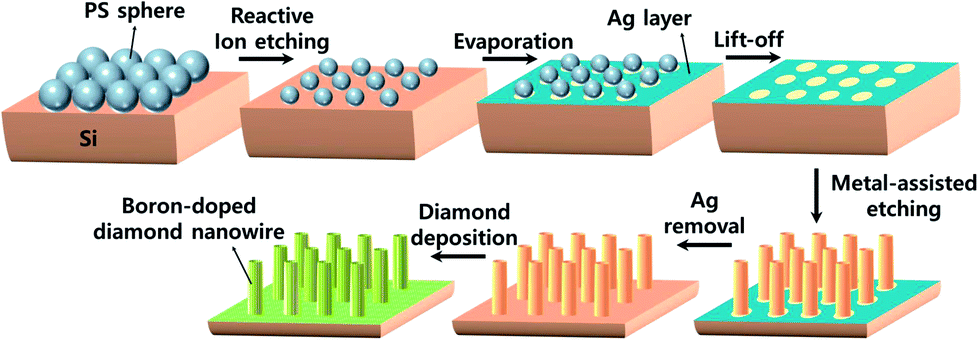 | ||
| Fig. 1 Schematic illustration of the BDDNW array electrode fabrication process. | ||
2.3. Characterization and measurements
The microstructures and electrochemical properties of the BDDNW and BDDNW array electrodes were analyzed. Field-emission scanning electron microscopy (FESEM, Hitachi S-4300) was used to examine the surface morphology of the electrodes. Raman spectra were obtained using a 514.5 nm Ar-ion laser. A potentiostat (Princeton Applied Research, VersaSTAT3) with a three-electrode cell of platinum, Ag/AgCl and a BDD electrode representing the counter, reference and working electrodes, respectively, was used for electrochemical analyses.To evaluate the bulk oxidation performance of the electrode, we constructed a single-compartment electrolytic circulation cell that operates in galvanostatic mode. The BDD electrodes and a stainless steel plate were used as the anode and the cathode, respectively; the areas of electrodes were 4 × 4 cm2. The target organic compound was 1.0 mM phenol in a 0.5 M Na2SO4 electrolyte (1 L). The current density was fixed at 30 mA cm−2, and the total flow rate was 1 L min−1. For the mass-transfer-limiting condition, the distance between the parallel electrodes was fixed at 1 cm, which is a much greater distance than that used in our previous study (0.5 mm).23 During the 3 h of electrolysis, a 2 mL sample was extracted at each data point. From the extracted samples, the phenol concentration (HPLC), the COD (Hach DR-5000), the current efficiency and the specific energy consumption were determined.
3. Results and discussion
3.1. Physical characterization
For the periodic BDDNW array, soft lithography was used for the self-assembly of PS sphere templates Fig. 2(a) and (b) shows the PS sphere monolayer self-assembled using spin coating. With adjustment of various parameters such as the PS sphere colloidal concentration, the spin speed and the step time, a highly ordered hexagonal-packed PS sphere monolayer was formed.38 Although some vacancies and misfit planes are observed, the PS monolayer successfully coats the entire Si substrate (4 cm × 4 cm). During the RIE process at 450 W for 7 min, the 1 μm diameter of the PS spheres was decreased by 400 nm (Fig. 2(c)). Subsequently, a 40 nm-thick Ag film was thermally evaporated on the substrate as a catalyst. After the PS mask was removed ultrasonically, a Ag film with a hexagonal array of holes was formed, as shown in Fig. 2(d).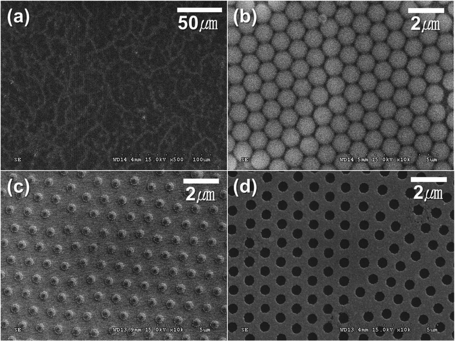 | ||
| Fig. 2 SEM images of the spin-coated PS sphere monolayer at (a) low magnification and (b) high magnification, (c) the size-reduced PS spheres by RIE, and (d) the Ag catalyst layer after ultrasonic removal of the PS masks. | ||
MACE of the Si process was conducted using a solution of DI water, HF and H2O2, resulting in the formation of the SiNW array (Fig. 3(a)). ESAND seeding and the HFCVD process were then carried out to deposit BDD. Fig. 3(b) and (d) shows the BDDNW array electrode. Diamond crystals a few hundred nanometers in size were formed along the etched Si surfaces. The length and thickness of the BDDNW array were observed to be 1 μm and 500 nm, respectively. The ESAND seeding method provides dense nanodiamond seeding on a complex nanotextured Si substrate without physical damage, which leads to the deposition of thin and smooth nanocrystalline BDD.23,39,40 In the case of BDDNW, the average length and thickness of the wires is 750 nm and 200 nm, respectively. The smaller diameter of the nanowires in BDDNW may provide advantages in terms of the surface area. Most importantly, the randomly etched Si substrate had a much smaller interspace between the wires (ca. 80 nm) and a much higher wire density than the BDDNW array (500 nm); thus, the BDDNW surface had a much larger geometric surface area.
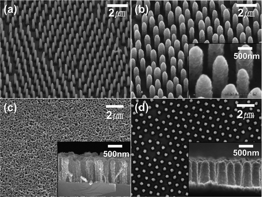 | ||
| Fig. 3 SEM images of (a) the SiNW array (30° tilted top-view), (b) the BDDNW array (30° tilted top-view), (c) top and cross-section (inset) view of the BDDNW and (d) top and cross-section (inset) view of the BDDNW array. | ||
Fig. 4 shows the Raman spectra of the BDD electrodes. The spectra of all the BDD electrodes had nanocrystalline diamond peaks at approximately 1130 cm−1 and diamond peak at 1320–1332 cm−1.41 Compared with the spectrum of the planar BDD in previous study, the spectra of both the BDDNW and the BDDNW array showed a lower intensity at 1332 cm−1 band, which is attributed to the sp3 crystalline diamond phase, and a large G peak (1550–1600 cm−1), which is attributed to sp2 amorphous carbon.42,43 Although the crystalline sp3 diamond phase portion decreased, the larger crystal population and additional grain boundaries of the BDDNW and the BDDNW array enhanced their electrochemical properties, as measured by their electro-oxidation performance.
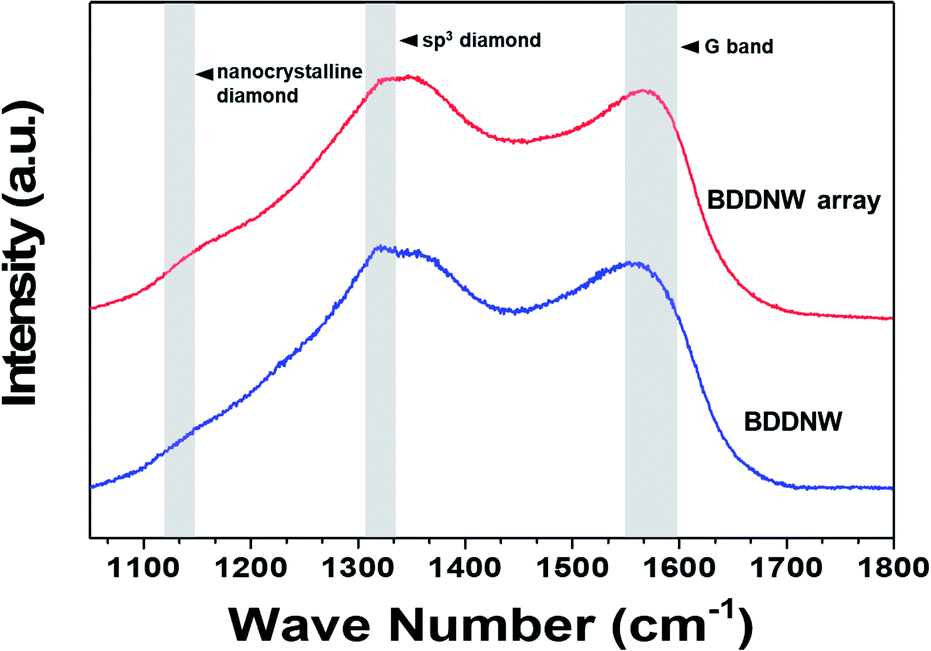 | ||
| Fig. 4 Raman spectra of the electrodes. | ||
3.2. Electrochemical characterization
To examine the electrochemical performance of the BDD electrodes in the absence of a flow, CV and chronocoulometry were conducted without any stirring or pumping. Fig. 5(a) shows the cyclic voltammograms obtained at a scan rate of 50 mV s−1 in 3 M KCl containing 10 mM Fe(CN)63−/4−. Both the BDDNW and the BDDNW array showed significantly higher peak currents and lower peak-to-peak separation potentials (ΔEp) compared to the planar BDD electrode in previous study, which are attributed to the large surface area of the nanowire structure. Comparing the BDDNW and the BDDNW arrays, the BDDNW shows a slightly larger peak current and a lower ΔEp. The anodic and cathodic peak current of the BDDNW electrode are 2.63 mA and −2.38 mA, respectively. In the case of the BDDNW array electrode, the anodic and cathodic peak current values are 2.38 mA and −2.34 mA, respectively. This higher peak current suggest that the electrochemically active surface area is larger and that the electron transfer kinetics and the electrochemical activity of the electrode are better than that of the BDDNW array in the absence of a flow.44 To evaluate the electrochemical effective surface area, chronocoulometry was conducted (Fig. 5(b)). The electrochemical effective surface area of the BDD electrodes was calculated on the basis of the following equation:where n is the number of electrons in the redox reaction, A is the electrode surface area, c is the substrate concentration, D is the diffusion coefficient (7.6 × 10⁻⁶ cm2 s−1), Qdl is the double-layer charge, and Qads is the faradic charge.45 The calculated effective surface area per unit area (1 cm2) of the BDDNW and BDDNW array electrodes are 14.11 cm2 cm−2 and 11.78 cm2 cm−2, respectively. The nanowires, with their high aspect ratio, contributed to the enhancement of the effective surface area of the electrodes. A comparison of the BDDNW and BDDNW array electrodes reveals that, despite the much higher density of the nanowire, the BDDNW shows only a 20% enhanced effective surface area compared with the BDDNW array. Although the BDDNW electrode has a larger geometric surface area, it does not have a fully activated surface region because of the very narrow nanowire interspaces, resulting in a large difference between the geometric area and the effective surface area. Nevertheless, the CV and chronocoulometry results indicate that the BDDNW with dense nanowires exhibits better performance than the BDDNW array, at least in the absence of a flow.
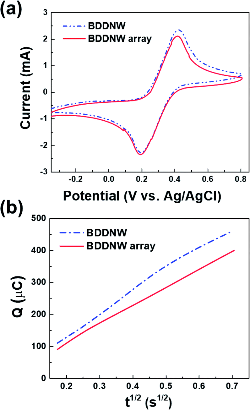 | ||
| Fig. 5 (a) Cyclic voltammograms of the BDDNW and BDDNW array with 10 mM Fe(CN)63−/4− in 3 M KCl and (b) Q–t1/2 curves of the BDDNW and BDDNW array with 0.1 mM K3[Fe(CN)6] in a 1 mM KCl solution. | ||
Under flow conditions, somewhat different results were obtained. We evaluated the mass transfer coefficient by the limiting-current technique in a constant electrolyte flow situation. In a plot of the current versus the applied potential, the plateau region of oxidation of a known substance was determined to be the limiting-current (Ilim).46 The mass transfer coefficient (k) was calculated from the following equation:
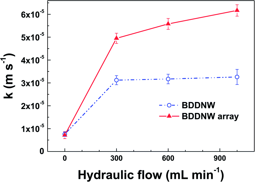 | ||
| Fig. 6 The mass transfer coefficient of the electrodes at different hydraulic flow rates. | ||
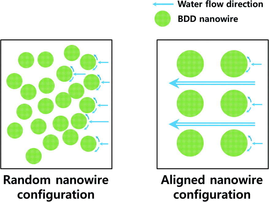 | ||
| Fig. 7 Schematic of the water flow on the electrode surfaces. | ||
3.3. Bulk electrolysis
To evaluate the electro-oxidation performance, we conducted bulk electrolysis of 1 mM phenol using a single-compartment electrolytic cell with a flow rate of 1 L min−1. Fig. 8(a) and (b) show decreases in the phenol concentration and the COD as a function of the specific charge amount on the BDDNW and BDDNW array electrodes. The rate of phenol removal and the COD exponentially decrease during electrolysis, as predicted by electrochemical oxidation theory.48 Under the mass-transport-limiting situation, which implies a low molecule concentration and high current density, the main phenol decomposition mechanism is the production of hydroxyl radicals on the anode surface, which can maximize the effect of the electrode surface area and electro-oxidation kinetics on the oxidation performance.48 A comparison of the BDDNW and BDDNW array electrodes shows that the BDDNW array electrode exhibits a higher removal rate for phenol and a higher COD despite the smaller effective surface area. These results indicate that both the effective surface area and the mass transfer coefficient are important parameters for the flowing bulk electrolysis performance under mass-transport-limiting conditions.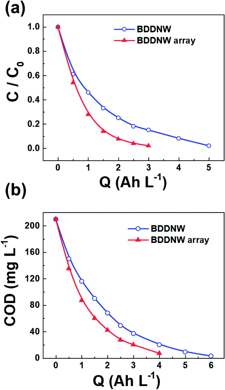 | ||
| Fig. 8 (a) Phenol and (b) COD removal behavior on different electrodes. | ||
Fig. 9(a) shows the instantaneous current efficiency (ICE) as a function of the specific charge amount on the BDDNW and BDDNW array electrodes. The ICE for the anodic oxidation of phenol was calculated using the following equation:
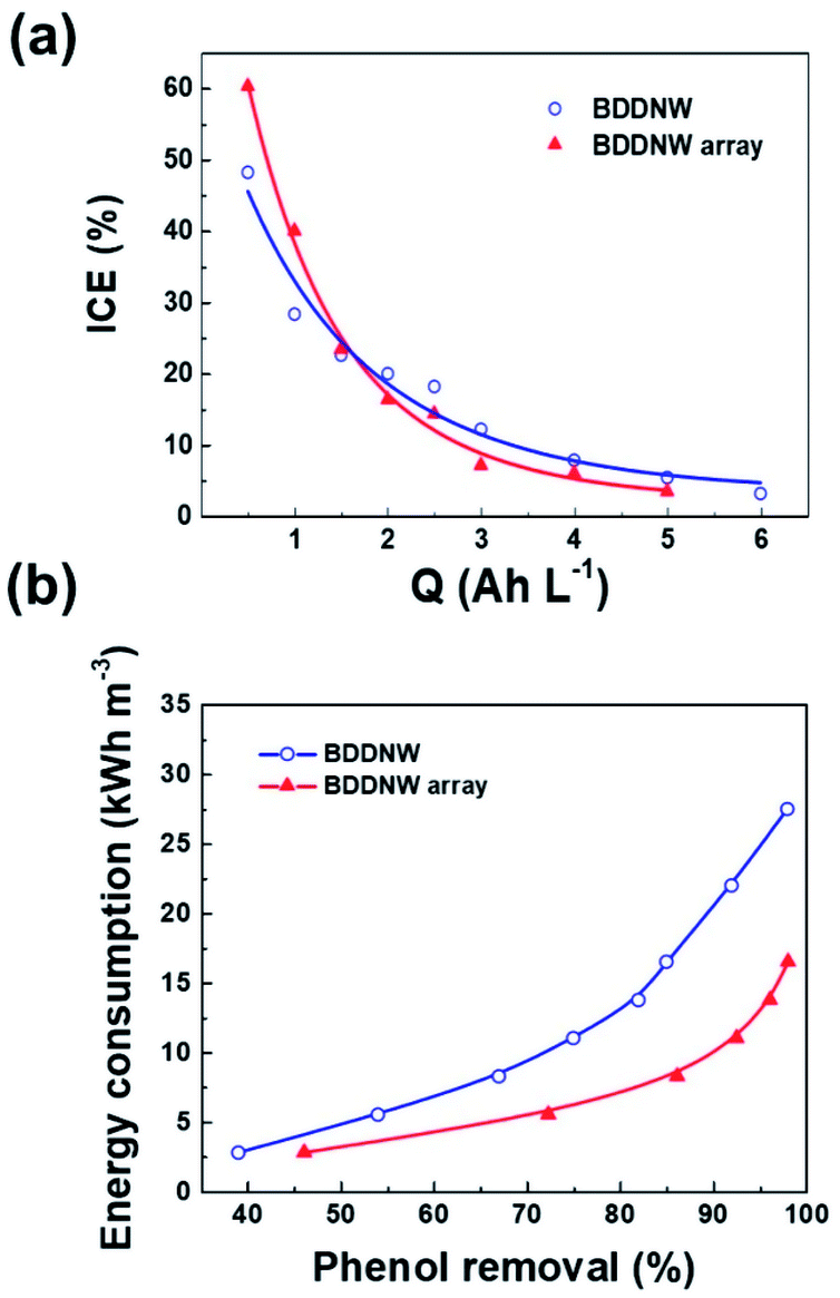 | ||
| Fig. 9 (a) ICE as a function of specific charge and (b) specific energy consumption as a function of phenol removal on different electrodes. | ||
| Anode | Initial concentration (mg L−1) | Current density (mA cm−2) | Electrolyte | Electrode distance (mm) | Flow rate (L min−1) | Charge (A h L−1) | Phenol removal (%) | COD removal (%) | ICE (%) | GCEa (%) | Reference |
|---|---|---|---|---|---|---|---|---|---|---|---|
a  . . |
|||||||||||
| BDD | 94 | 15 | Na2SO4 (0.5 M) | — | — | 3.37 | 100 | >88 | <15 | — | Sun et al.50 |
| BDD | 471 | 60 | HClO4 (1 M) | 10 | 2.7 | 14 | >80 | — | <10 | — | Iniesta et al.48 |
| BDD | 280 | 50 | Na2SO4 (0.3 M) | 5 | — | 5.6 | — | >90 | — | — | Souza et al.51 |
| BDD | 1882 | 142 | H2SO4 (0.1 M) | 10 | 3.3 | 20 | — | >90 | — | — | Weiss et al.52 |
| BDD | 81 | 30 | Na2SO4 (0.5 M) | 0.5 | 1 | 3 | 91 | 85.6 | 8 | 18.5 | Lee et al.23 |
| BDDNW array | 94 | 30 | Na2SO4 (0.5 M) | 10 | 1 | 3 | 98.3 | 90.5 | 7.1 | 21.2 | This study |
4. Conclusions
By using a PS sphere mask and MACE of a Si template, a highly ordered BDDNW array electrode was successfully fabricated. Compared to BDDNW with a random nanowire configuration, the BDDNW array showed a somewhat smaller effective surface area; however, it had a higher mass transfer coefficient by a factor of two under flow conditions. In the bulk electrolysis of phenol-containing water, the BDDNW array electrode showed a much faster phenol and COD removal rate as well as a higher current efficiency. With its high mass transfer rate, the BDDNW array electrode exhibited highly enhanced electrochemical oxidation performance compared with the BDDNW electrode in our previous study. These results indicate that a high mass transfer rate in a flow-by operational electrode can be achieved not by a simple enlargement of the surface area but by a careful microscopic surface design strategy that considers the surface flow dynamics. The efficiency of BDDNW array may be further increased with optimizing nanowire array design in future work. With a large effective surface area and a high mass transfer rate, the BDDNW array electrode may solve the problem of the productivity and performance of BDD and may have future applications in wastewater treatment.Conflicts of interest
There are no conflicts to declare.Acknowledgements
This work was supported by Korea Ministry of Environment (MOE) as “Public Technology Program based on Environmental Policy” (No. E416-00070-0604-0).References
- T. N. Rao, I. Yagi, T. Miwa, D. A. Tryk and A. Fujishima, Anal. Chem., 1999, 71, 2506–2511 CrossRef CAS PubMed.
- N. Vinokur, B. Miller, Y. Avyigal and R. Kalish, J. Electrochem. Soc., 1996, 143, L238–L240 CrossRef CAS.
- G. M. Swain, A. B. Anderson and J. C. Angus, MRS Bull., 1998, 23, 56–60 CrossRef CAS.
- A. Sugitani, M. Katayama, T. Watanabe, Y. Matsumoto and Y. Einaga, RSC Adv., 2013, 3, 25636–25639 RSC.
- J. Svitkova, T. Ignat, L. Svorc, J. Labuda and J. Barek, Crit. Rev. Anal. Chem., 2016, 46, 248–256 CrossRef CAS PubMed.
- N. J. Yang, J. S. Foord and X. Jiang, Carbon, 2016, 99, 90–110 CrossRef CAS.
- P. A. Michaud, M. Panizza, L. Ouattara, T. Diaco, G. Foti and C. Comninellis, J. Appl. Electrochem., 2003, 33, 151–154 CrossRef CAS.
- A. Benito, A. Penades, J. L. Lliberia and R. Gonzalez-Olmos, Chemosphere, 2017, 166, 230–237 CrossRef CAS PubMed.
- P. K. Jiwanti, K. Natsui, K. Nakata and Y. Einaga, RSC Adv., 2016, 6, 102214–102217 RSC.
- X. M. Chen, G. H. Chen, F. R. Gao and P. L. Yue, Environ. Sci. Technol., 2003, 37, 5021–5026 CrossRef CAS PubMed.
- Y. P. He, W. M. Huang, R. L. Chen, W. L. Zhang, H. B. Lin and H. D. Li, Sep. Purif. Technol., 2015, 156, 124–131 CrossRef CAS.
- C. A. Martinez-Huitle, M. A. Quiroz, C. Comninellis, S. Ferro and A. De Battisti, Electrochim. Acta, 2004, 50, 949–956 CrossRef CAS.
- N. Oturan, J. Wu, H. Zhang, V. K. Sharma and M. A. Oturan, Appl. Catal., B, 2013, 140, 92–97 CrossRef.
- J. Roeser, N. F. A. Alting, H. P. Permentier, A. P. Bruins and R. Bischoff, Anal. Chem., 2013, 85, 6626–6632 CrossRef CAS PubMed.
- A. Gicquel, K. Hassouni, F. Silva and J. Achard, Curr. Appl. Phys., 2001, 1, 479–496 CrossRef.
- C. Chen, E. Nurhayati, Y. Juang and C. Huang, J. Environ. Sci., 2016, 45, 100–107 CrossRef PubMed.
- R. Bogdanowicz, A. Fabianska, L. Golunski, M. Sobaszek, M. Gnyba, J. Ryl, K. Darowicki, T. Ossowski, S. D. Janssens, K. Haenen and E. M. Siedlecka, Diamond Relat. Mater., 2013, 39, 82–88 CrossRef CAS.
- C. K. Mavrokefalos, M. Hasan, W. Khunsin, M. Schmidt, S. A. Maier, J. F. Rohan, R. G. Compton and J. S. Foord, Electrochim. Acta, 2017, 243, 310–319 CrossRef CAS.
- F. L. Souz, C. Saez, M. R. V. Lanza, P. Canizares and M. A. Rodrigo, Electrochim. Acta, 2016, 187, 119–124 CrossRef.
- N. J. Yang, H. S. Uetsuka, E. Sawa and C. E. Nebel, Nano Lett., 2008, 8, 3572–3576 CrossRef CAS PubMed.
- N. J. Yang, H. Uetsuka and C. E. Nebel, Adv. Funct. Mater., 2009, 19, 887–893 CrossRef CAS.
- J. F. Zhang, T. Nakai, M. Uno, Y. Nishiki and W. Sugimoto, Carbon, 2014, 70, 207–214 CrossRef CAS.
- C. H. Lee, E. S. Lee, Y. K. Lim, K. H. Park, H. D. Park and D. S. Lim, RSC Adv., 2017, 7, 6229–6235 RSC.
- D. B. Luo, L. Z. Wu and J. F. Zhi, ACS Nano, 2009, 3, 2121–2128 CrossRef CAS PubMed.
- S. K. Lee, M. J. Song, J. H. Kim, T. S. Kan, Y. K. Lim, J. P. Ahn and D. S. Lim, NPG Asia Mater., 2014, 6, e115 CrossRef CAS.
- H. Zanin, P. W. May, D. J. Fermin, D. Plana, S. M. C. Vieira, W. I. Milne and E. J. Corat, ACS Appl. Mater. Interfaces, 2014, 6, 990–995 CAS.
- Y. P. He, W. M. Huang, R. L. Chen, W. L. Zhang and H. B. Lin, J. Electroanal. Chem., 2015, 758, 170–177 CrossRef CAS.
- Y. P. He, W. M. Huang, R. L. Chen, W. L. Zhang and H. B. Lin, Sep. Purif. Technol., 2015, 149, 124–131 CrossRef CAS.
- J. D. Wang, T. T. Li, M. M. Zhou, X. P. Li and J. M. Yu, Electrochim. Acta, 2015, 173, 698–704 CrossRef CAS.
- B. P. Chaplin, Environ. Sci.: Processes Impacts, 2014, 16, 1182–1203 CAS.
- M. A. Oturan and J. J. Aaron, Crit. Rev. Environ. Sci. Technol., 2014, 44, 2577–2641 CrossRef CAS.
- A. M. Zaky and B. P. Chaplin, Environ. Sci. Technol., 2013, 47, 6554–6563 CrossRef CAS PubMed.
- F. C. Moreira, R. A. R. Boaventura, E. Brillas and V. J. P. Vilar, Appl. Catal., B, 2017, 202, 217–261 CrossRef CAS.
- Y. P. He, H. B. Lin, X. Wang, W. M. Huang, R. L. Chen and H. D. Li, Chem. Commun., 2016, 52, 8026–8029 RSC.
- F. Gao and C. E. Nebel, ACS Appl. Mater. Interfaces, 2016, 8, 18640–18646 CAS.
- S. Ruffinatto, H. A. Girard, F. Becher, J. C. Amault, D. Tromson and P. Bergonzo, Diamond Relat. Mater., 2015, 55, 123–130 CrossRef CAS.
- J. H. Kim, S. K. Lee, O. M. Kwon and D. S. Lim, J. Nanosci. Nanotechnol., 2009, 9, 4121–4127 CrossRef CAS PubMed.
- P. Colson, R. Cloots and C. Henrist, Langmuir, 2011, 27, 12800–12806 CrossRef CAS PubMed.
- S. K. Lee, J. H. Kim, M. G. Jeong, M. J. Song and D. S. Lim, Nanotechnology, 2010, 21, 505302 CrossRef PubMed.
- J. H. Kim, S. K. Lee, O. M. Kwon, S. I. Hong and D. S. Lim, Diamond Relat. Mater., 2009, 18, 1218–1222 CrossRef CAS.
- K. Siuzdak, R. Bogdanowicz, M. Sawczak and M. Sobaszek, Nanoscale, 2015, 7, 551–558 RSC.
- J. V. Macpherson, Phys. Chem. Chem. Phys., 2015, 17, 2935–2949 RSC.
- P. W. May, W. J. Ludlow, M. Hannaway, P. J. Heard, J. A. Smith and K. N. Rosser, Chem. Phys. Lett., 2007, 446, 103–108 CrossRef CAS.
- X. H. Kang, J. Wang, H. Wu, I. A. Aksay, J. Liu and Y. H. Lin, Biosens. Bioelectron., 2009, 25, 901–905 CrossRef CAS PubMed.
- F. C. Anson, Anal. Chem., 1964, 36, 932–934 CrossRef CAS.
- P. Canizares, J. Garcia-Gomez, I. F. de Marcos, M. A. Rodrigo and J. Lobato, J. Chem. Educ., 2006, 83, 1204–1207 CrossRef CAS.
- X. P. Zhu, J. R. Ni, H. N. Li, Y. Jiang, X. A. Xing and A. G. L. Borthwick, Electrochim. Acta, 2010, 55, 5569–5575 CrossRef CAS.
- J. Iniesta, P. A. Michaud, M. Panizza, G. Cerisola, A. Aldaz and C. Comninellis, Electrochim. Acta, 2001, 46, 3573–3578 CrossRef CAS.
- C. Comninellis and C. Pulgarin, J. Appl. Electrochem., 1991, 21, 703–708 CrossRef CAS.
- J. R. Sun, H. Y. Lu, H. B. Lin, L. L. Du, W. M. Huang, H. D. Li and T. Cui, Sep. Purif. Technol., 2012, 88, 116–120 CrossRef CAS.
- R. B. A. de Souza and L. A. M. Ruotolo, Int. J. Electrochem. Sci., 2013, 8, 643–657 Search PubMed.
- E. Weiss, K. Groenen-Serrano and A. Savall, J. Appl. Electrochem., 2008, 38, 329–337 CrossRef CAS.
| This journal is © The Royal Society of Chemistry 2018 |