
 Open Access Article
 This Open Access Article is licensed under a
 Creative Commons Attribution 3.0 Unported Licence
CH3NH3Pb1−xEuxI3 mixed halide perovskite for hybrid solar cells: the impact of divalent europium doping on efficiency and stability†
Xiaowei Wu a,
Hongwei Li*a,
Kai Wangb,
Xiaowei Sunb and
Liduo Wang*c
a,
Hongwei Li*a,
Kai Wangb,
Xiaowei Sunb and
Liduo Wang*c
aNational Engineering Research Center for Rare Earth Materials, General Research Institute for Nonferrous Metals, Grirem Advanced Materials Co., Ltd., Beijing, 100088, China. E-mail: lihw0923@vip.126.com
bDepartment of Electrical & Electronic Engineering, Southern University of Science and Technology of China, Shenzhen, 518055, China
cKey Lab of Organic Optoelectronics and Molecular Engineering of Ministry of Education, Department of Chemistry, Tsinghua University, Beijing 100084, China. E-mail: chldwang@mail.tsinghua.edu.cn
First published on 20th March 2018
Abstract
The crucial role of the impact of divalent europium doping in perovskite solar cells is investigated in this work. We selected europium (Eu2+, 117 pm) to replace lead (Pb2+, 119 pm) because their ion radii are really comparable. This appropriate substitution has shown great potential to achieve high stability and enhance the power conversion efficiency of the solar cells. Through adjusting the doping concentration of europium, the perovskite solar cells corresponding average efficiency greatly increased. Furthermore, compared with the CH3NH3PbI3 perovskite film, the attenuation of power conversion efficiency of europium doped perovskite film slowed down 4.7 times at room temperature. Therefore, we put forward a useful method for the optimization of organic–inorganic perovskite solar cells.
Introduction
The recently arisen organic–inorganic halide hybrid perovskite, as a star in the family of multifunctional materials, has attracted extensive interest from both scientific and industrial communities. The materials are applied in many fields, such as photovoltaics,1,2 photodetectors,3,4 light-emitting diodes,5 lasers,6,7 and electrochromism.8 Organic–inorganic hybrid halide perovskite materials are commonly based on the ABX3 structure, where A is a monovalent cation (methylammonium (MA+), formamidinium (FA+), etc.), B is a divalent metal ion (Pb2+, Sn2+, Ge2+, Sr2+, Cd2+, Ca2+, etc.), and C is a monovalent anion (Cl−, Br−, I−, SCN−, etc.). This kind of material possesses several advantages such as low cost solution processability, large absorption coefficients, tunable band-gaps, high extinction coefficients, long carrier lifetimes, and high carrier mobility.9–14 In the past few years, the power conversion efficiency (PCE) of perovskite-based solar cells (PSCs) increased rapidly from 3.8% to 22.1% accompanied with the development of the large-area module processing techniques,15–18 which almost caught up with or even exceed the efficiency of crystalline silicon, CIGSe (copper–indium–gallium–selenide) and CdTe solar cells.19–21 In order to achieve the high performance and better stability of the solar cell, the perovskite thin film should be pinhole-free, grain boundary cracks-free, smooth, dense and well-defined crystalline.22–28 As a result, various methods were developed to improve these qualities of perovskite thin film, for example interfacial engineering, solvent engineering, additive-assisted preparation, etc.29–34Doping of semiconductors, a process of intentional inserting impurities into an extremely pure crystal, is a key approach to manipulate optical and electrical properties of device.35–39 In general, new energy states within the band gap are introduced by doping, so as to facilitate the occurrence of low-energy electronic transitions.35,40,41 MAPbX3 are primarily doped by the elements isovalent with cations (Li+/Na+/Rb+), anions (I−/Cl−) or metal cations (Pb2+/M2+, M2+ = Sn2+, Sr2+, Cd2+, Zn2+ or Ca2+).9,34,42–47 In lead halide perovskites, MA and Pb cations are surrounded by 12 and 6 halide anions, respectively, which makes it to be a superb candidate to accommodate a variety of foreign ions with ionic radii comparable that of MA or Pb. However, this phenomenon limits the dopants' capacity, so as to change the majority charges from positive to negative or impact the concentration of the majority charge carriers.39
The previous work reported that the ions (Bi3+, Li+, Na+, K+, Rb+) are doped into the halide perovskites, just as a topotactic insertion.38,39,41,42,48 On one hand, the successfully incorporating dopants into perovskite crystals, and preserving the host lattice structures simultaneously, only cause tiny lattice distortion. On the other hand, these dopants oppose oxidation and reduction owing to their stability or resistance hence are chosen to be the positive additive.39 Nevertheless, there are, still many other elements not been explored.
Rare earth (RE) is a special down-conversion functional material. RE cation, as an activation center or dopants, has been widely used in automobile catalysts, petroleum refining catalysts, phosphors in color television and flat panel display, permanent magnets, rechargeable batteries for hybrid and electric vehicles, numerous medical devices.43 RE ions have the ability absorb UV light and re-emit visible light due to their specific 4f electronic structure.44–47 It is a kind of ideal candidate for extending the spectral response range of perovskite material to the UV region and enhancing the PSCs efficiency while reducing the UV degradation to improve the device stability.48 It was reported that in the dye sensitized solar cells (DSSCs), trivalent RE doping can reduce intra-gap trap states in anatase, which affects the electron diffusion length, and the low RE concentration in the lattice will affect the unit cell parameters in the structure. In the DSSCs, the doped Eu and Tb created an impurity energy level, giving rise to the absorbance spectra shift.46 Much research using RE to improve the PSCs performance of PSCs has been proposed.49–51 However, the influence of RE doping in the PSCs have not been reported yet.
Hence, based on the special properties of RE elements, we propose embedding Eu2+(117 pm), which is only slightly smaller than Pb2+(119 pm), into a photoactive perovskite phase.52,53 We introduced halide of rare earth EuI2 as a dopant embedded into MAPbI3. After doping, the absorbance of the thin film changed, since the Eu2+ has many different energy level transition orbits, the absorbance of the thin film was improved through doping bivalent RE ion (Eu2+), and the fill factor (FF) increased caused by reducing the PbI2 phase precipitate and enlarging the grain size. The PCE of the device with efficiency of 16.7%, was significantly promoted with 25% compared with the control sample. And the perovskite stability was enhanced slightly in air because of the disappearance of bad phase of PbI2.
Experimental
Materials synthesis
Methylammonium iodide (CH3NH3I) was synthesized and purified based on the method proposed by J. H. Im.54 All chemicals were used as received. Methylammonium iodide (CH3NH3I) was synthesized by mixing methylamine (CH3NH2) (27.8 mL, 0.273 mol, 40 wt% in methanol, Alfa Aesar) and hydroiodic acid (HI) (30 mL, 0.227 mol, 57 wt% in water, Alfa Aesar) in a 250 mL round-bottom flask, and stirring the mixture in an ice-water bath for 2 h. The yellowish raw product obtained by evaporating the solvent was recrystallized three times from a mixture of diethyl ether and ethanol. After filtration, the solid was collected in a dark container and dried at 60 °C in a vacuum oven overnight. Anhydrous EuI2 was synthesized and purified based on the method proposed by Chengpeng D.55 Anhydrous EuI2 was prepared by dissolving europium oxide (Eu2O3) and ammonium iodide (NH4I) into HI to form a transparent solution. We obtained a dense solid after we evaporated the solution. Then the solid was placed into a quartz tube for vacuum dehydration in a tube heating furnace, until it was completely dehydrated. After that, the dehydrated solid was sintered until the solid turned to transparent melt. Eventually, anhydrous EuI2 in bulk polycrystalline was obtained.Fabrication of solar cells
Devices were fabricated on fluorine-doped tin oxide (FTO) coated glass (Yingkou OPV Tech New Energy CO., LTD., OPV-FTO22-7). Initially, FTO was etched with 2 mol L−1 HCl solution and zinc metal powder. Substrates were then cleaned sequentially by soap solution (2 vol% Hellmanex™ detergent), deionized water, acetone, ethanol, isopropanol (IPA) and UV exposure. Nickel(II) acetylacetonate was dissolved in ethanol (0.1 mol L−1) with adding 5.3 μL ethanolamine (38 wt%) into the solution. The solution was then stirred in a sealed glass vial in air overnight. Then the NiO solution was spin-coated onto the UV–ozone treated FTO substrate at 3000 rpm for 60 s and then annealed at 400 °C for 60 min in ambient.The perovskite thin film was deposited by using a process similar to that described in a previous work.47 The MAPbI3![[thin space (1/6-em)]](https://www.rsc.org/images/entities/char_2009.gif) :x% EuI2 (x = 0, 0.02, 0.04, 0.06, 0.08, 0.1) precursor solution was prepared by dissolving CH3NH3I (1 mmol), PbI2 (1.05 mmol; Alfa Aesar, 99.9985%) and EuI2 (a corresponding mass fraction of PbI2) in g-butyrolactone (GBL)/dimethyl sulfoxide (DMSO) (7:3; 1 mL) with a total concentration of 1 M and stirring at 70 °C overnight. The perovskite thin films spread with 80 μL was spin coated onto the FTO/NiO substrate followed by a two-stage spin-coating process at 1000 rpm for 15 s and 4000 rpm for 45 s. Then chlorobenzene (600 μL; Alfa Aesar, 99%) was dripped as anti-solvent after 25 s the second stage to obtain a light-brown smooth film. Afterward, the perovskite film was annealed at 100 °C for 10 min to convert to a dark-brown film. Subsequently, PCBM (15 mg dissolved in 1 mL chlorobenzene) was deposited on the cooled perovskites substrates by spin coating at 1500 rpm for 45 s, followed by the spin coating of BCP saturated solution in isopropanol. Finally, silver electrode (70 nm thick) was thermally evaporated on top of the device under high vacuum (<1 × 10⁻⁴ Pa). The active area of the device was 0.090 cm2, defined by the aperture area of the metal shadow mask.
:x% EuI2 (x = 0, 0.02, 0.04, 0.06, 0.08, 0.1) precursor solution was prepared by dissolving CH3NH3I (1 mmol), PbI2 (1.05 mmol; Alfa Aesar, 99.9985%) and EuI2 (a corresponding mass fraction of PbI2) in g-butyrolactone (GBL)/dimethyl sulfoxide (DMSO) (7:3; 1 mL) with a total concentration of 1 M and stirring at 70 °C overnight. The perovskite thin films spread with 80 μL was spin coated onto the FTO/NiO substrate followed by a two-stage spin-coating process at 1000 rpm for 15 s and 4000 rpm for 45 s. Then chlorobenzene (600 μL; Alfa Aesar, 99%) was dripped as anti-solvent after 25 s the second stage to obtain a light-brown smooth film. Afterward, the perovskite film was annealed at 100 °C for 10 min to convert to a dark-brown film. Subsequently, PCBM (15 mg dissolved in 1 mL chlorobenzene) was deposited on the cooled perovskites substrates by spin coating at 1500 rpm for 45 s, followed by the spin coating of BCP saturated solution in isopropanol. Finally, silver electrode (70 nm thick) was thermally evaporated on top of the device under high vacuum (<1 × 10⁻⁴ Pa). The active area of the device was 0.090 cm2, defined by the aperture area of the metal shadow mask.
Characterizations
X-ray diffraction (XRD) patterns were obtained with Smart LAB instruments CuKα beam (λ = 1.54 Å). UV-vis absorption spectra measurement was carried out on a Hitachi U-3010 spectroscope, and was employed to assess the absorption properties of the doped perovskite sensitized NiO thin film. The morphology of the film was tested with scanning electron microscopy (SEM; JEOL JSM-7401F). The incident photon-to-electron conversion efficiency (IPCE) spectra were measured in air with equipment developed by the Institute of Physics, Chinese Academy of Sciences.The energy dispersive X-ray spectroscope (EDS) combined with a field-emission scanning electron microscope (SEM-EDS, EDAX Octane Pro). X-ray energies corresponded to I, Pb and Eu were collected as the SEM scanned the electron beam over the surface and cross-sectional area in FTO substrate. The X-ray data was synchronized with the SEM image and an ‘element image’ was created showing the presence of the selected element throughout the selected area.
The current density–voltage (J–V) curves were measured with a 2400 Series SourceMeter (Keithley Instruments) under simulated AM 1.5 sunlight at an equivalent to 100 mW cm−2 irradiance generated by an thermo oriel 91192-1000 simulator, with the intensity being calibrated with an VLSI standards incorporated PN 91150V Si reference cell. The mismatch factor was calculated to be less than 1%. The solar cells were masked with a metal aperture to define the active area, typically 0.090 cm2. The backward bias for stability characterization of the solar cell was held to 0.75 V. The as-prepared solar cells were stored at 25 °C in light with a relative humidity (RH) of 30 ± 5% for the characterization of ambience stability. The specific PCE as a function of time was obtained with conventional environment treatment for 13 days in order to clarify the PCE evolution of solar cells.
Results and discussion
The simple schematic diagram of our working is showed in Fig. 1 The schematic architecture of the perovskite solar cells (PSCs) and the energy band diagram of the PSCs, exhibit the collecting process of photo-generated carriers, which specific numerical referenced those reported.56,57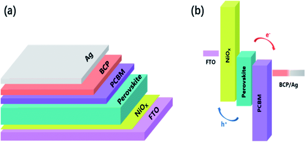 | ||
| Fig. 1 (a) The schematic architecture of the perovskite solar cells (PSCs). (b) Energy-level diagram of the PSCs, exhibiting the collecting process of photo-generated carriers. | ||
Fig. 2 shows the absorbance result of the perovskite film with or without Eu2+ doped. Fig. 2(a) demonstrates the evolution of the UV-vis absorbance of perovskite films with or without doped of different EuI2 concentrations. Compared with the control sample, the absorbance of doped perovskite is enhanced especially in the 350–540 nm. The normalized absorbance at 521 nm is listed with different amount of EuI2 as the dopant in the MAPbI3, as shown in Fig. 2(b). At the doping concentration of 0.06%, the film exhibits the maximum absorbance. However, for the wavelength larger than 540 nm, only the perovskite film with 0.04% doped in MAPbI3 has an obvious improvement. As the result of our measurement, the concentration of 0.04% being doped in MAPbI3 achieves the highest efficiency. This probably because the rare earth Eu2+ in MAPbI3 can form a new impurity energy level, causing the absorbance spectra shift to lower energy region.58 It is commonly known that substances always tend to transfer to lower energy states, since the lower energy level is, the more stable substances will be.59 Thereby the erosion of the perovskite is slightly shifted as well as the similar phenomenon observed in de Quilettes D. W. work.48 As presented in Fig. 2(c), the IPCE values are significantly enhanced by doping Eu2+. Fig. 2(d) gives the J–V curves of the perovskite solar cells measured at backward scan direction, and the corresponding photovoltaic performance parameters are listed in Table 1, which consists with the improvement of UV-vis absorption and IPCE.
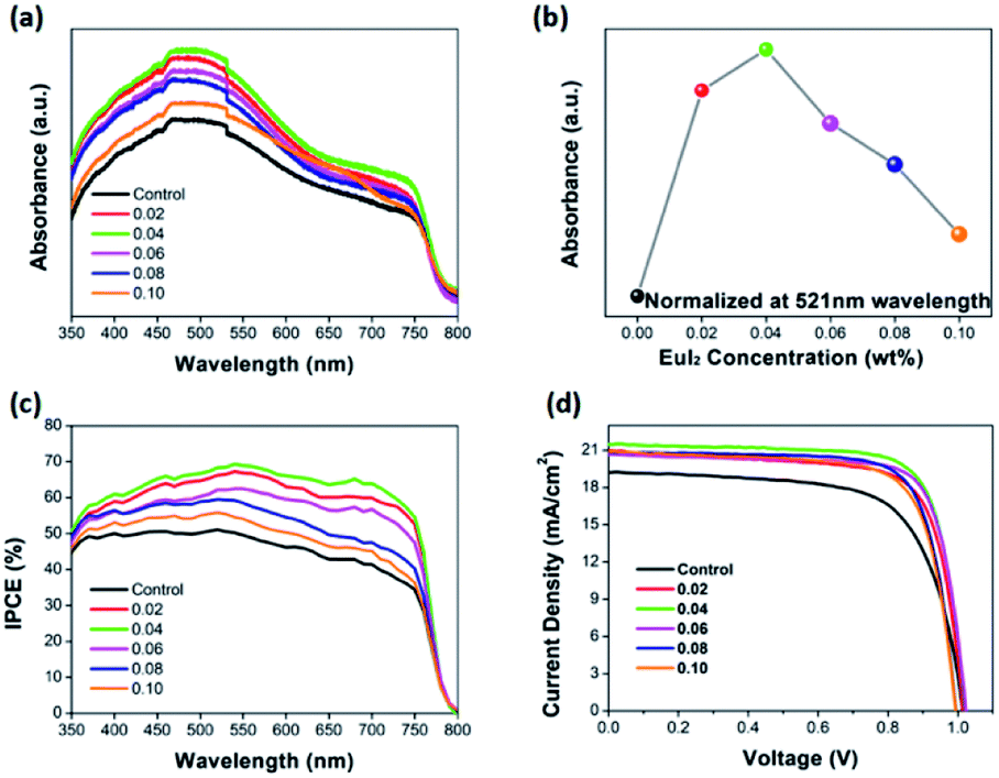 | ||
| Fig. 2 (a) UV-vis absorption spectra of the pristine and Eu2+-doped perovskite films. (b) The normalized absorbance at 521 nm. (c) The IPCE spectra. (d) J–V curves of the best-performing device without and with EuI2 doped at a scan rate of 0.10 s−1 under simulated sunlight irradiance. | ||
| Device | Jsc (mA cm−2) | Voc (V) | FF | PCE (%) |
|---|---|---|---|---|
| Control | 19.2 | 1.02 | 0.678 | 13.3 |
| 0.02 | 20.9 | 1.02 | 0.731 | 15.6 |
| 0.04 | 21.5 | 1.02 | 0.764 | 16.7 |
| 0.06 | 20.7 | 1.02 | 0.778 | 16.4 |
| 0.08 | 20.9 | 1.00 | 0.758 | 15.8 |
| 0.10 | 20.9 | 1.00 | 0.733 | 15.3 |
The changes of thin film crystal structure were verified by an XRD instrument. Fig. 3 and S1† shows that both the thin films with and without EuI2 doping can form the typical tetragonal perovskite structure. The RE dopants do not have any significant effect on the crystallization of perovskite. Whereas the PbI2 diffraction peak in the XRD pattern is disappeared with EuI2 being doped, proving a slightly decrease of the unreacted PbI2. Elimination of the PbI2 block would effectively improve the crystal boundary contact. On one hand, the hardly existed PbI2 phase increase the FF and then raises the PCE of the device. On the other hand, the compact grain boundary reduces the corrosion rate of perovskite thin film and then enhances the stability of the device.
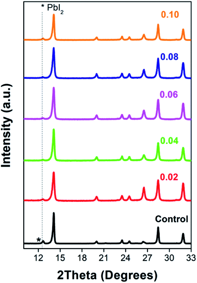 | ||
| Fig. 3 XRD patterns of the PSCs with and without EuI2 doped. Gray dash line depicts the position of PbI2. | ||
Scanning electron microscopy (SEM) was conducted to characterize the morphology and crystallinity of the prepared perovskite films. Fig. 4 (Fig. S2†) exhibits the top-view SEM images of the perovskite thin films prepared by adjusting the EuI2 concentration to tune the coverage of the film. For the control perovskite film, apparent pin-holes can be seen. It is widely known that pin-hole in the perovskite thin film will cause severe carrier recombination and deteriorate the efficiency of device. The defects not only make the electrons and holes meet directly at selective layer, but also immensely affect the absorbance.60–62 When the EuI2 as a dopant inserts into the perovskite layer, the grain size of the perovskite thin film is enlarged. When the doping concentration is 0.04 wt%, the grain size obviously larger than the pristine. Combining the XRD results, we conclude that the introducing of EuI2 as a dopant in the planar perovskite can improve both the film uniformity and the perovskite crystallinity, which are two key prerequisites for high performance and stable perovskite solar cells.63 In addition, when the doping concentration is 0.08 wt%, the grain into dendritic crystals, because crystallization rate is too fast to form independent grain.64,65
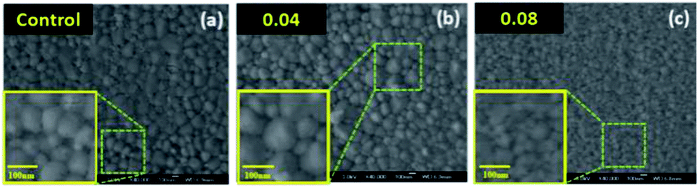 | ||
| Fig. 4 Top-down SEM images of perovskite thin films prepare by different EuI2 concentrations. | ||
To further investigate the electron trap-state density in the perovskite absorber, we fabricated electron-only devices (FTO/SnO2/MAPb1−xEuxI3/PCBM/Ag). Fig. 5 shows the typical dark J–V characteristics of the electron-only and hole-only device based on different perovskites. The linear relation indicates an ohmic response of the device at low bias corresponds. The current increased linearly with the voltage up to a clear konk point. The current shows a more rapid rise, when the voltage increased to the region over the kink-point, demonstrating that filling of the trap states by injected carriers. The trap densities can be determined by the trap-filled limit voltage (VTFL) which called the space charge limited current (SCLC) technique. The trap density can be calculated by the equation:66 VTFL = entL2/2 εεo, where nt is the trap-state density, L is the perovskite film thickness, ε and εo represent the elementary charge and vacuum permittivity, respectively. And the relative dielectric constant of MAPbI3 ε is 28.8,67 the thickness of measures films is 250 nm. After fitting, the VTFL of the control, 0.04, and 0.08 are 0.3, 0.1 and 0.2 V, respectively. Therefore, the corresponding electron trap density is 8.06 × 1015 cm−3 for the control perovskite film. When the perovskite with Eu2+ doped at 0.04%, the electron trap density is reduced to 2.67 × 1015 cm−3, indicating that the film quality is improved. The reduced electron trap density contributed to reducing the J–V hysteresis in the perovskite with Eu doped device.
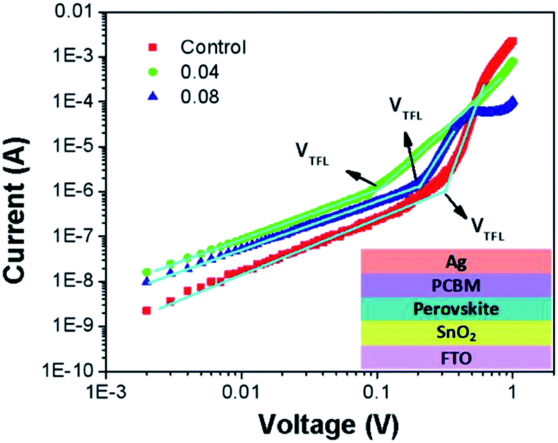 | ||
| Fig. 5 Dark I–V characteristics of the electron only device displaying VTFL kink point behavior (inset shows the device structure). | ||
The hysteresis of J–V curves, which affected by the defect states or the band bending, is an important issue to determined the actual PCE. As shown in Fig. 6(a), while the devices with Eu doping, the J–V hysteresis is eliminated. That might be associated with two reasons, one is the large grain formation caused by the doping with Eu, leading to enhanced the film quality, and the other is PbI2 phase disappearing which reduced film defects. Table 2 summarizes the key J–V parameters of PSCs device using both reverse and forward scan conditions. In order to further confirm that there is no hysteresis indeed for the device with Eu doping and ensure the J–V measurement is reliable, the photocurrent density and PCE of the champion device were recorded as a function of time, as shown in Fig. 6(b). The photocurrent density and steady-state power output of the champion device with the doping concentration of 0.04%, remained stable within 100 s, and a highly stable PCE at 16.7% can be obtained.68
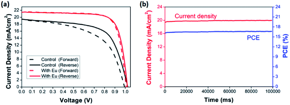 | ||
| Fig. 6 (a) J–V curves measured under both forward and reverse scan mode for the devices based on with and without Eu doping in MAPbI3. (b) The steady-state power and photocurrent density output as a function of time at the maximum power output values for champion device. | ||
| device | Scan direction | Jsc (mA cm−2) | Voc (V) | FF | PCE (%) |
|---|---|---|---|---|---|
| Control | Reverse | 19.26 | 0.99 | 0.689 | 13.4 |
| Forward | 19.45 | 1.03 | 0.635 | 12.7 | |
| 0.04 | Reverse | 21.50 | 1.02 | 0.763 | 16.7 |
| Forward | 21.56 | 1.01 | 0.762 | 16.4 |
As mentioned above, an optimized amount of EuI2 is beneficial for the formation of high performance and stable perovskite thin films. The photovoltaic performance of perovskite solar cells prepared with pristine perovskite thin films and EuI2-doped perovskite thin films were further studied. As shown in Fig. 7, the FF and Jsc are improved obviously when EuI2 is applied, leading to a substantially improvement of average PCE from 13.3% to 16.7%. The statistical PCE data are obtained from 200 devices of different batches. It is demonstrated by several studies that the large grain size could achieve high performance.69–73 Some excellent reviews described two primary benefits of growing crystals with large grain size. One is the reduced interfacial area associated with large grains suppresses charge trapping and eliminates hysteresis. The other is larger grains have lower bulk defects and higher mobility, allowing the photo induced carriers propagate through the device without frequent encounters with defects and impurities.71 As can be seen from Fig. 4, when the doping concentration maintained in a certain range, the grain size has been was enlarged. While the crystals morphology becomes poor again when the EuI2 content reaches 0.08%, due to phase separation resulting from immiscibility, and grew into dendritic crystal.56,70,71
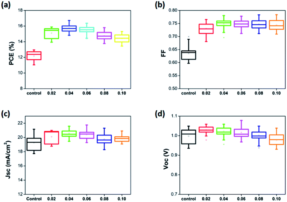 | ||
| Fig. 7 Photovoltaic characteristics for the PSCs with EuI2 doped of different concentrations (statistics of data for 10 batches of the device). | ||
The normalized data of stabilized power output of the cells was shown Fig. 8. We studied the conventional environment stability of the devices, and the PCEs were measured every day. The aging test was carried out at the temperature of 25 °C and RH of 25 ± 5%. For the pristine devices, the PCE decrease nearly 48.05% in 288 h. With 0.04% of EuI2 doped, the top PCE only reduce by 10.25%, and maintains almost 90%. With the increase of doping concentration, the stability of the device can be improved. But if the doping concentration is too large, the stability begin to decline. As our previous analysis, the doped crystal hardly has any PbI2 phase precipitates, which can improve the thin film uniformity and the perovskite crystallinity. And the crystal of enlarged grain denser, make the grain boundary have less flaws, hence obtaining a high quality crystalline. High quality crystalline states not only can improve the PCE and FF, but also promote the stability of device. As we all know, seed crystals can speed up the crystallization and induce the grain boundary with less defects, which can reduce the rate of corrosion. Therefore, so our work results show the consequence that the stability of solar cells is enhanced. Furthermore, there was a positive correlation between the grain boundary area and corrosion rate, since the larger area is, the faster corrosion rate.74,75 For the crystal growing into dendrite, the grain boundary area is too large, thus the stability is lower, which is keeping with our test results.
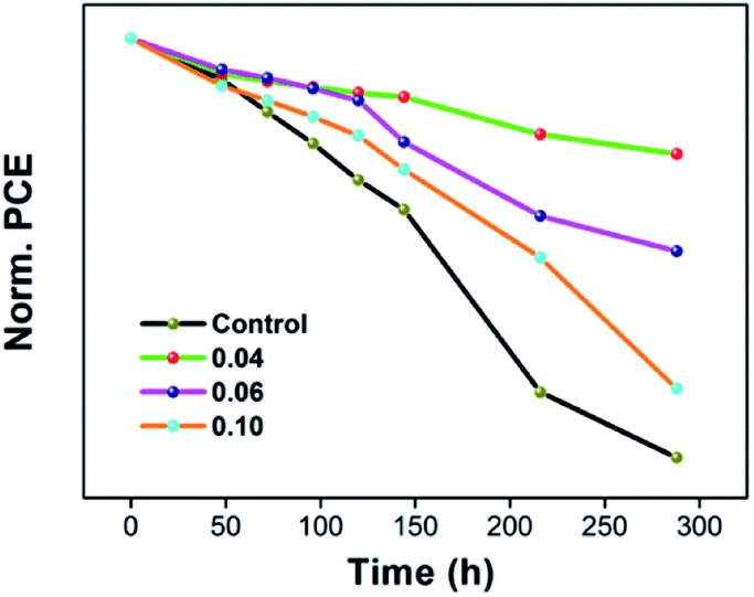 | ||
| Fig. 8 The normalized data of stabilized power output of the cells. | ||
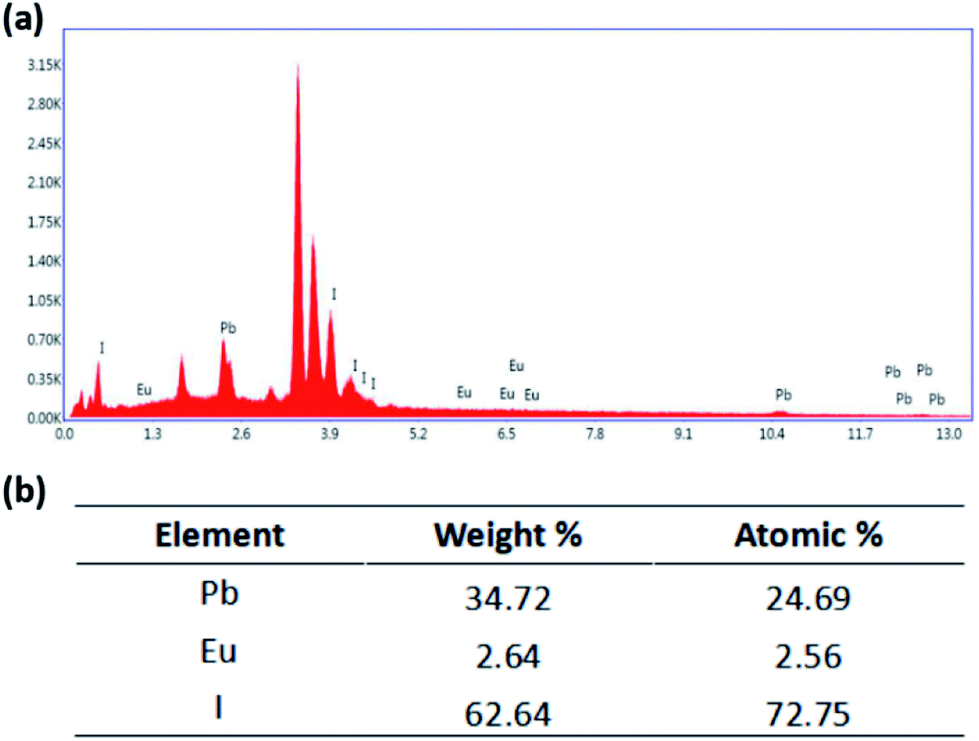
In order to characterize the doping of Eu2+, the SEM-EDS measurement was conducted as shown in Fig. 9. It shows the surface EDS mapping (Fig. S3†), where Pb and I are well distributed three-dimensionally in the FTO film. As shown in Fig. 7, weight percentages from EDS elemental analysis of the film surface are found to be 34.72%, 2.64% and 62.64% for Pb, Eu, and I, respectively, which correspond to 24.69%, 2.56% and 72.75% in atomic percentage. This indicates that the ratio of Pb and Eu to I is 1:3, which consists with the atomic ratio in the ABX3 structure.
 | ||
| Fig. 9 EDS results of the perovskite film on FTO substrate. | ||
Conclusions
In conclusion, we inserted an anhydrous EuI2 as a dopant into the perovskite to control the perovskite crystal grain size and reduce the PbI2 phase of the perovskite thin film. Inserting RE elements of Eu into MAPbI3 is favorable to realize of a dense perovskite film with a nearly whole coverage and larger grain size. We successfully used this method to improve the FF of the inverted planar perovskite solar cells. The best performing device, using an extremely low doping ratio 0f 0.04 EuI2 as the dopant in MAPbI3, achieves a PCE of 16.7% with a high Jsc of 21.5 mA cm−2 and an enhanced FF of 0.763, which is much higher than the control device without any dopants. Meanwhile, EuI2 as a dopant greatly enhances the stability of the perovskite films. This study provides significant development towards the critical role of the RE as dopants utilizing in photovoltaic devices, and helps to boost the performance of the inverted planar perovskite solar cells to be a higher efficient and more stable state.Conflicts of interest
There are no conflicts to declare.Acknowledgements
Chengpeng Diao, Jinqiu Yu, Nan Li and Qingshun Dong contributed equally to this work. The research was funded by the National Natural Science Foundation of China (No. 51402021).Notes and references
- H. S. Kim, C. R. Lee and J. H. Im, et al., Sci. Rep., 2012, 2, 591 CrossRef PubMed.
- M. Liu, M. B. Johnston and H. J. Snaith, Nature, 2013, 501, 395–398 CrossRef CAS PubMed.
- L. Dou, Y. M. Yang and J. You, et al., Nat. Commun., 2014, 5, 5404 CrossRef CAS PubMed.
- I. Suárez, E. J. Juárez-Pérez and J. Bisquert, et al., Adv. Mater., 2015, 27, 6157–6162 CrossRef PubMed.
- Y. H. Kim, H. Cho and J. H. Heo, et al., Adv. Mater., 2015, 27, 1248–1254 CrossRef CAS PubMed.
- F. Deschler, M. Price and S. Pathak, et al., J. Phys. Chem. Lett., 2014, 5, 1421–1426 CrossRef CAS PubMed.
- G. Xing, N. Mathews and S. S. Lim, et al., Nat. Mater., 2014, 13, 476–480 CrossRef CAS PubMed.
- Q. Jiang, M. Chen and J. Li, et al., ACS Nano, 2017, 11, 1073–1079 CrossRef CAS PubMed.
- J. Navas, A. Sánchez-Coronilla and J. J. Gallardo, et al., Nanoscale, 2015, 7, 6216–6229 RSC.
- Y. Zhao and K. Zhu, J. Phys. Chem. Lett., 2014, 5, 4175–4186 CrossRef CAS PubMed.
- G. E. Eperon, V. M. Burlakov and P. Docampo, et al., Adv. Funct. Mater., 2014, 24, 151–157 CrossRef CAS.
- D. Shi, V. Adinolfi and R. Comin, et al., Science, 2015, 347, 519–522 CrossRef CAS PubMed.
- C. C. Stoumpos, C. D. Malliakas and M. G. Kanatzidis, Inorg. Chem., 2013, 52, 9019–9038 CrossRef CAS PubMed.
- M. I. Saidaminov, A. L. Abdelhady and B. Murali, et al., Nat. Commun., 2015, 6, 7586 CrossRef PubMed.
- A. Kojima, K. Teshima and Y. Shirai, et al., J. Am. Chem. Soc., 2009, 131, 6050–6051 CrossRef CAS PubMed.
- National Renewable Energy Laboratory (NREL), Best Research-Cell Efficiencies Chart (as of March 2016).
- M. Saliba, T. Matsui and J. Y. Seo, et al., Energy Environ. Sci., 2016, 9, 1989–1997 CAS.
- J. Burschka, F. Kessler and M. K. Nazeeruddin, et al., Chem. Mater., 2013, 25, 2986–2990 CrossRef CAS.
- M. Saliba, T. Matsui and J. Y. Seo, et al., Energy Environ. Sci., 2016, 9, 1989–1997 CAS.
- X. Li, D. Bi and C. Yi, et al., Science, 2016, 353, 58–62 CrossRef CAS PubMed.
- H. S. Kim, S. H. Im and N. G. Park, J. Phys. Chem. C, 2014, 118, 5615–5625 CAS.
- X. Cao, C. Li and Y. Li, et al., Nanoscale, 2016, 8, 19804–19810 RSC.
- B. Cai, W. H. Zhang and J. Qiu, Chin. J. Catal., 2015, 36, 1183–1190 CrossRef CAS.
- T. Gershon, B. Shin and N. Bojarczuk, et al., Adv. Energy Mater., 2015, 5, 2 Search PubMed.
- Z. Tong, C. Yan and Z. Su, et al., Appl. Phys. Lett., 2014, 105, 223903 CrossRef.
- W. Li, J. Fan and J. Li, et al., J. Am. Chem. Soc., 2015, 137, 10399–10405 CrossRef CAS PubMed.
- Y. K. Ren, X. H. Ding and Y. H. Wu, et al., J. Mater. Chem. A, 2017, 5, 20327–20333 CAS.
- Y. Ren, B. Duan and Y. Xu, et al., Sci. China Mater., 2017, 60, 392–398 CrossRef CAS.
- S. Bag and M. F. Durstock, ACS Appl. Mater. Interfaces, 2016, 8, 5053–5057 CAS.
- Q. Dong, Z. Wang and K. Zhang, et al., Nanoscale, 2016, 8, 5552–5558 RSC.
- W. Zhang, S. Pathak and N. Sakai, et al., Nat. Commun., 2015, 6, 10030 CrossRef CAS PubMed.
- L. Zhao, D. Luo and J. Wu, et al., Adv. Funct. Mater., 2016, 26, 3508–3514 CrossRef CAS.
- N. Li, H. Dong and H. Dong, et al., J. Mater. Chem. A, 2014, 2, 14973–14978 CAS.
- Y. Shi, X. Wang and H. Zhang, et al., J. Mater. Chem. A, 2015, 3, 22191–22198 CAS.
- D. Mocatta, G. Cohen and J. Schattner, et al., Science, 2011, 332, 77–81 CrossRef CAS PubMed.
- S. M. Sze, Semiconductor devices: physics and technology, John Wiley & Sons, 2008 Search PubMed.
- Y. Piao, B. Meany and L. R. Powell, et al., Nat. Chem., 2013, 5, 840–845 CrossRef CAS PubMed.
- C. Ehli, C. Oelsner and D. M. Guldi, et al., Nat. Chem., 2009, 1, 243–249 CrossRef CAS PubMed.
- M. Saliba, T. Matsui and K. Domanski, et al., Science, 2016, 354, 206–209 CrossRef CAS PubMed.
- A. L. Abdelhady, M. I. Saidaminov and B. Murali, et al., J. Phys. Chem. Lett., 2016, 7, 295–301 CrossRef CAS PubMed.
- Y. Zhou, Z. J. Yong and K. C. Zhang, et al., J. Phys. Chem. Lett., 2016, 7, 2735–2741 CrossRef CAS PubMed.
- N. Vicente and G. Garcia-Belmonte, J. Phys. Chem. Lett., 2017, 8, 1371–1374 CrossRef CAS PubMed.
- S. D. Stranks, G. E. Eperon and G. Grancini, et al., Science, 2013, 342, 341–344 CrossRef CAS PubMed.
- P. Strange, A. Svane and W. M. Temmerman, et al., Nature, 1999, 399, 756–758 CrossRef CAS.
- F. Auzel, Chem. Rev., 2004, 104, 139–174 CrossRef CAS PubMed.
- G. Wu, L. Zhang and B. Cheng, et al., J. Am. Chem. Soc., 2004, 126, 5976–5977 CrossRef CAS PubMed.
- J. Jin, H. Li and C. Chen, et al., ACS Appl. Mater. Interfaces, 2017, 9, 42875–42882 CAS.
- D. W. de Quilettes, S. M. Vorpahl and S. D. Stranks, et al., Science, 2015, 348, 683–686 CrossRef CAS PubMed.
- N. Chander, A. F. Khan and P. S. Chandrasekhar, et al., Appl. Phys. Lett., 2014, 105, 033904 CrossRef.
- X. Hou, T. Xuan and H. Sun, et al., Sol. Energy Mater. Sol. Cells, 2016, 149, 121–127 CrossRef CAS.
- W. Chen, Q. Luo and C. Zhang, et al., J. Mater. Sci. Mater. Electron., 2017, 28, 11346 CrossRef CAS.
- R. D. Shannon, Acta Crystallogr., 1976, 32, 751–767 CrossRef.
- G. Pan, X. Bai and D. Yang, et al., Nano Lett., 2017, 17, 8005–8011 CrossRef CAS PubMed.
- J. H. Im, C. R. Lee, J. W. Lee, S. W. Park and N. G. Park, Nanoscale, 2011, 3, 4088–4093 RSC.
- D. Chengpeng, Y. U. Jinqiu and L. I. Hongwei, et al., J. Rare Earths, 2015, 33, 1189–1195 CrossRef.
- Z. Bin, J. Li and L. Wang, et al., Energy Environ. Sci., 2016, 9, 3424–3428 CAS.
- J. Li, W. Li and H. Dong, et al., J. Mater. Chem. A, 2015, 3, 8882–8889 CAS.
- C. Chen, H. Li and J. Jin, et al., Adv. Energy Mater., 2017, 7, 1700758 CrossRef.
- T. Peng, L. Huajun, H. Yang and C. Yan, Mater. Chem. Phys., 2004, 85, 68 CrossRef CAS.
- L. Zhao, D. Luo and J. Wu, et al., Adv. Funct. Mater., 2016, 26, 3508–3514 CrossRef CAS.
- W. Li, W. Zhang and S. Van Reenen, et al., Energy Environ. Sci., 2016, 9, 490–498 CAS.
- M. B. Johnston and L. M. Herz, Acc. Chem. Res., 2015, 49, 146–154 CrossRef PubMed.
- R. Kobayashi, Phys. D, 1993, 63, 410–423 CrossRef.
- Z. Xiao, Q. Dong and C. Bi, et al., Adv. Mater., 2014, 26, 6503–6509 CrossRef CAS PubMed.
- J. F. Shackelford, Chem. Eng., 1999, 11, 41 Search PubMed.
- R. H. Bube, J. Appl. Phys., 1962, 33, 1733–1737 CrossRef CAS.
- A. Poglitsch and D. Weber, J. Chem. Phys., 1987, 87, 6373 CrossRef CAS.
- C. Chen, H. Li and J. Jin, et al., Nano Energy, 2017, 32, 165–173 CrossRef CAS.
- M. Liu, M. B. Johnston and H. J. Snaith, Nature, 2013, 501, 395–398 CrossRef CAS PubMed.
- Q. Chen, H. Zhou and Z. Hong, et al., J. Am. Chem. Soc., 2013, 136, 622–625 CrossRef PubMed.
- W. Nie, H. Tsai and R. Asadpour, et al., Science, 2015, 347, 522–525 CrossRef CAS PubMed.
- W. J. Yin, J. H. Yang and J. Kang, et al., J. Mater. Chem. A, 2015, 3, 8926–8942 CAS.
- H. Choi, J. Jeong and H. B. Kim, et al., Nano Energy, 2014, 7, 80–85 CrossRef CAS.
- D. T. J. Hurle, Handbook of crystal growth, North Holland, 1993 Search PubMed.
- K. A. Jackson, Kinetic Processes: Crystal Growth, Diffusion, and Phase Transformations in Materials, John Wiley & Sons, 2006 Search PubMed.
Footnote |
| † Electronic supplementary information (ESI) available. See DOI: 10.1039/c7ra12754e |
| This journal is © The Royal Society of Chemistry 2018 |