DOI:
10.1039/C8RA00384J
(Review Article)
RSC Adv., 2018,
8, 10489-10508
Large-area perovskite solar cells – a review of recent progress and issues
Received
13th January 2018
, Accepted 5th March 2018
First published on 14th March 2018
Abstract
In recent years, perovskite solar cells (PSCs) have attracted great attention in the photovoltaic research field, because of their high-efficiency (certified 22.1%) and low-cost. In this review paper, we briefly introduce the history of efficiency development for PSCs, and discuss some of the major problems for large-area (≥1 cm2) PSC devices. In addition, we summarize the recent progress in the aspects of fabrication methods for large-area perovskite films, and improving the efficiency and stability of the large-area PSC devices. Finally, we give a short summary and outlook of large-area PSC devices. This article is mainly organized into three parts. The first part focuses on the main fabricating technologies for large-area perovskite films. The second section discusses some methods that are used to improve the efficiency of PSCs. In the last part, different approaches are used to improve the stability of PSCs.
1. Introduction
Due to the growing population, the global energy demand is increasing year by year. Moreover, the global energy demand is predicted to double by 2050.1,2 Thus, the development of renewable energy becomes an imminent requirement, such as water energy, wind energy, and solar energy. The photovoltaic power generation capacity is installed to be 303 GW and increased 75 GW in 2016. In 2016, photovoltaic power generation accounted for only 1.5% of the world's total electricity generation. So high performance, long-term stability, low cost and environmental friendly solar cells become the focus of current energy research.
PSCs have attracted great attention in photovoltaic research in recent years, because of their high-efficiency (certified 22.1%)3 and low-cost. Meanwhile, organic–inorganic perovskites have a high optical absorption coefficient4 and the diffusion lengths exceed 1 μm for electrons and holes.5 So, organic–inorganic perovskite is an ideal absorber material for solar cells,6–19 photodetectors,20–22 light-emitting diodes,23–26 etc.
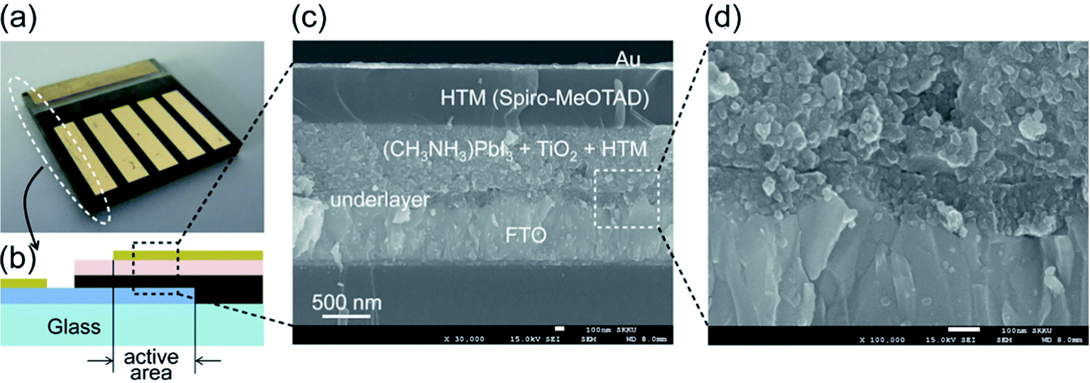
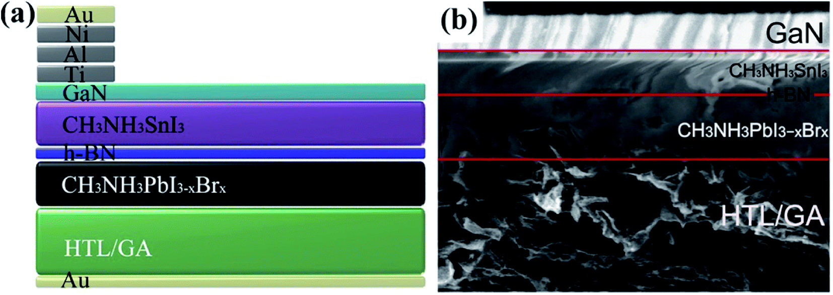
In recent years, hybrid metal halide perovskite materials have revolutionized the field of photovoltaics materials research, due to the power conversion efficiency (PCE) of PSC devices having been rapidly improved, from the point 3.8% in 2009,6 up to 22.6% in 2017 (ref. 3) (certified 22.1%).3 It attracted attention of researchers working on various photovoltaic technologies, especially dye solar cells (DSCs) and organic photovoltaic (OPV) with emphasis on better efficiency. In 2009, T. Miyasaka et al.6 has creatively made CH3NH3PbBr3/TiO2-based and CH3NH3PbI3/TiO2-based DSCs, the PCE of the cells is 3.13% and 3.81%, respectively. The PSCs attracted researchers' attention then happened in 2012, when M. Grätzel and N. G. Park et al.27 made PSCs device using perovskite films as the photoactive absorber layer, the mp-TiO2 and spiro-MeOTAD were used as the electron transport layer (ETL) and hole transport layer (HTL), respectively (Fig. 1), achieving the PCE of 9.7%. In 2013, M. Z. Liu, M. B. Johnston and H. J. Snaith8 fabricated planar heterojunction PSCs via vapor deposition, and the efficiency of the PSCs device is up to 15.4%. The yttrium (Y) doping the TiO2 (ETL) improves the electron transport channel in the PSCs device, and increase its carrier concentration and modify the ITO electrode to reduce its work function. These changes achieved a PCE of 19.3%.28 In 2015, S. I. Seok et al.29 attained an efficiency of PSCs up to 20.1%. In 2016, A. Zettl et al.30 made an architecture of GaN/CH3NH3SnI3/monolayer h-BN/CH3NH3PbI3−xBrx/HTL and graphene aerogel/Au (Fig. 2). The graded bandgap PSCs demonstrated with PCE averaging 18.4%, with a best of 21.7%. Other researchers, E. H. Sargent et al.31 (2017) achieved the certified efficiencies of 20.1% via contact-passivation strategy, retaining 90% (97% after dark recovery) of their initial PCE after 500 hours of continuous room-temperature. Meanwhile, E. K. Kim, J. H. Noh, and S. I. Seok et al.3 reported that the introduction of additional iodide ions into the organic cation solution, that was used to form the perovskite layers through an intramolecular exchanging process and decrease the concentration of deep-level defects. The certified PCE of PSCs attained 22.1%.3
 |
| | Fig. 1 (a) Real solid-state device. (b) Cross-sectional structure of the device. (c) Cross-sectional SEM image of the device. (d) Active layer–underlayer–FTO interfacial junction structure.27 | |
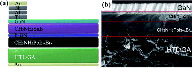 |
| | Fig. 2 (a) Cross-sectional schematic. (b) SEM images of perovskite cell with integral monolayer h-BN and graphene aerogel.30 | |
In addition, high efficiency PSCs devices include not only small devices, but also larger cells. A PSCs device with area of large-area (≥1 cm2) and maximum PCE of 20.5% (certified 19.7%) has been reported.3 Table 1 shows some results for large-area PSCs have been reported in the literatures.
Table 1 Summary of large-area perovskite solar cells
| PSCs configuration |
Cells area (cm2) |
Active area (cm2) |
PCE (%) |
Ref. |
| ITO/PEDOT:PSS/MAPbI3/PCBM/C60/BCP/Al |
1 |
1 |
12.2 |
32 |
| FTO/TiO2/MAPbI3/spiro-OMeTAD/Au |
1 |
1 |
11.7 |
33 |
| ITO/HTL/PFN/CH3NH3PbI3/PCBM/Al |
1 |
1 |
17.04 |
34 |
| FTO/TiO2/(FAPbI3)0.85(MAPbBr3)0.15/spiro-OMeTAD/Au |
1 |
1 |
18.32 |
35 |
| FTO/c-TiO2/me-TiO2/MAPbI3/spiro-OMeTAD/Au |
1 |
1 |
19.3 |
36 |
| FTO/bl-TiO2/mp-TiO2/perovskite/spiro-OMeTAD/Au |
1 |
1 |
19.6 (certified) |
37 |
| FTO/TiO2/me-TiO2:perovskite/perovskite/PTAA/Au |
1 |
1 |
19.7 (certified) |
3 |
| ITO/SnO2/(FAPbI3)1−x(MAPbBr3)x/spiro-OMeTAD/Au |
1 |
1 |
20.1 (certified) |
38 |
| ITO/TiO2/CH3NH3PbI3−xClx/spiro-OMeTAD/Au |
4 |
1 |
13.6 |
39 |
| FTO/c-TiO2/me-TiO2/perovskite/spiro-OMeTAD/Au |
1.01 |
1.01 |
16.61 |
40 |
| FTO/NiMgLiO/MAPbI3/PCBM/Ti(Nb)Ox/Ag |
1.02 |
1.02 |
16.2 (15 certified) |
41 |
| Anode/HEL/perovskite/gradient interlayer/ETL/cathode |
1.022 |
1.022 |
18.21 (certified) |
42 |
| FTO/c-TiO2/me-TiO2/perovskite/spiro-OMeTAD/Au |
1.05 |
1.05 |
15.89 |
43 |
| FTO/ZnO/MAPbI3/spiro-OMeTAD/Au |
1.10 |
1.10 |
3.08 |
44 |
| FTO/TiO2–Cl/FA0.85MA0.15PbI2.55Br0.45/spiro-OMeTAD/Au |
1.10 |
1.10 |
19.5 (certified) |
31 |
| SAM/PC61BM/MAPbI3/PTAA/Ag |
1.20 |
1.20 |
15.98 |
45 |
| ITO/PEDOT:PSS/MAPbI3/PCBM/C60/BCP/Al |
64.0 |
1.50 |
6.0 |
32 |
| ITO/PEDOT:PSS/(PEI)2(MA)n−1PbnI3n+1/PCBM/LiF/Ag |
2.32 |
2.32 |
8.77 |
46 |
| SAM/PC61BM/MAPbI3/PTAA/Ag |
5.04 |
5.04 |
12.79 |
45 |
| FTO/c-TiO2/TiO2 or MAPbI3/spiro-OMeTAD/Au |
10.1 |
10.1 |
10.4 |
47 |
| FTO/c-TiO2/me-TiO2/MAPbI3/spiro-OMeTAD/Au |
36.0 |
36.0 |
15.7 (12.1 certified) |
36 |
| FTO/c-TiO2/TiO2 or MAPbI3/spiro-OMeTAD/Au |
100 |
100 |
4.3 |
47 |
But, for large-area PSCs device, it still has some issues need to be solved, namely fabrication, stability, hysteresis, fabrication cost and environmental concerns. Such as, the continuous fabrication of cracks-free and pinholes-free the perovskite and the selective carrier extraction layers films is difficulty with large-area PSCs devices. The dilemma with optimizing such charge carrier extraction layers in solar cells is that the film should be thin to minimize resistive losses, while at the same time, it should cover the entire collector area in a contiguous and uniform manner.48 In the large-area PSCs device, surfaces, bulk defects and interfaces introduce recombination centers that lead to fast nonradiative losses,49 and interface losses, which lead to the Voc, Jsc and fill factor (FF) decrease. Meanwhile, the perovskite material is easily thermal decomposition and hydrodecomposition, that leads to the lack of stability for PSCs device. The poor stability of the perovskite materials and devices is a big challenge, which hinder the PSCs device could be transferred from the laboratory to industry and outdoor applications. Thus, for large-area PSCs device, the major challenges relate to the improving efficiency and keeping the stability of the device. In this review paper, giving an update of the PSCs field, briefly, introducing the history of PSCs and then focus on the key progress of the fabrication, improving the efficiency and the stability of the large-area PSCs device.
2. Perovskite structure and typical PSCs structure
2.1 Perovskite structure and characteristics
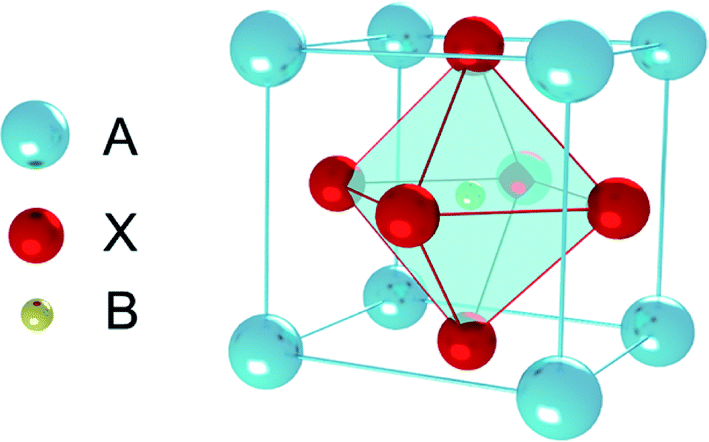
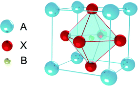
Perovskite was discovered in 1839, which originally referred to a kind of ceramic oxides with the general molecular formula ABX3.1 Recently, PSCs absorber layer is mainly organic–inorganic perovskite layer, the general molecular formula is also ABX3 (Fig. 3), where A is an organic cation (i.e. CH3NH3+, NH2CH![[double bond, length as m-dash]](https://www.rsc.org/images/entities/char_e001.gif) NH2+, CH3CH2NH3+), B is metal cation (i.e. Pb2+, Sn2+, Ge2+) and X is halogen anion (i.e. F−, Cl−, Br−, I−), are the most relevant ones for PSCs.
NH2+, CH3CH2NH3+), B is metal cation (i.e. Pb2+, Sn2+, Ge2+) and X is halogen anion (i.e. F−, Cl−, Br−, I−), are the most relevant ones for PSCs.
 |
| | Fig. 3 ABX3 perovskite structure. | |
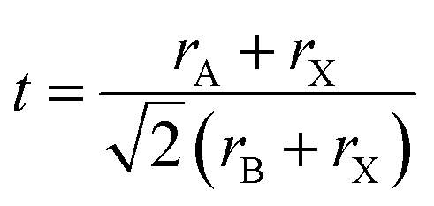
The perovskite arrangement is approximated on its geometric tolerance factor (t),
| |
 | (1) |
where
rA,
rB and
rX are the efficient ionic radius for A, B and X ions, respectively. When the
t = 1.0, the perovskite is a perfect cubic perovskite.
50 However, octahedral distortion is assessed when
t < 1, which influences electronic characteristics.
51 For alkali metal halide perovskite, formability is anticipated for 0.813 <
t < 1.107.
50,51 In
Table 2, the
rA in APbX
3 (X = Cl, Br, I) perovskite has been calculated for
t = 0.8 and
t = 1 based on effective ionic radii.
51 As the tolerance of CH
3NH
3PbI
3 (MAPbI
3) is 0.83, in this manner, the deviation from a perfect cubic structure is likely to happen.
50,51
Table 2 Estimation of A cation radii in APbX3
| rPba |
Xa |
rAb for t = 0.8 |
rAb for t = 1.0 |
Effective ionic radii for coordination number of 6. 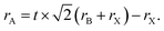 50,51 50,51 |
| Pb2+ (1.19 Å) |
Cl− (rCl = 1.81 Å) |
1.58 Å |
2.43 Å |
| Br− (rBr = 1.96 Å) |
1.60 Å |
2.50 Å |
| I− (rI = 2.20 Å) |
1.64 Å |
2.59 Å |
In the visible range, for the MAPbI3, the effective absorption coefficient is around 1.0 × 10⁵ (mol L−1)−1 cm−1 at 550 nm,4,52 when the thickness of perovskite films range is 500–600 nm, it can absorb complete light in films. Meanwhile, organic–inorganic perovskite exhibits better charge transfer characteristics. H. J. Snaith et al.5 reported the diffusion lengths (LD) of the electrons and holes in MAPbI3 and MAPbI3−xClx, the LD of MAPbI3 is 130 nm (electrons) and 100 nm (holes) and this of MAPbI3−xClx is 1100 nm (electrons) and 1200 nm (holes), respectively.5 So, the organic–inorganic perovskite is an ideal absorber layer material for solar cells.
2.2 Typical PSCs structure
Some of the typical structures of PSCs are shown in Fig. 4. The typical PSCs structures include the mesoporous structure (Fig. 4(a)), the planar heterojunction structure (Fig. 4(b)) and the inverted planar heterojunction structure (Fig. 4(c)). PSCs with regular configuration is transparent conductive oxide (TCO)/blocking layer (electron transport layer (ETL))/perovskite absorber layer/hole transport layer (HTL) material/gold (Au). The widely accepted a simplified operation principle of PSCs is presented as: perovskite absorber layer absorbs light and generates charges while the light on the PSCs. The electrons and holes pairs are created by the thermal energy, which diffuse and get separate through electron and hole selective contacts, respectively (Fig. 4(d)).53 Once electrons and holes are present at the cathode and anode, respectively, external load can be powered by connecting a circuit through it.
 |
| | Fig. 4 Different structural configurations of PSCs, (a) mesoporous structure, (b) planar heterojunction structure, (c) inverted planar heterojunction structure and (d) schematic of electron and hole transportation. | |
TiO2 is the most common ETL material,3,6,7,54 meanwhile, other ETL materials have been used to attain over 10% efficiencies (e.g. ZnO,13,55,56 SnO2,57–59 PCBM,60–65 LBSO,66 etc.). Spiro-OMeTAD is the widely used HTL material,35,57,67 the certified PCE of 22.1% in small cells.3 Meanwhile, other HTL materials have been used to achieve over 10% efficiencies (e.g. PTAA,29,66,68 P3HT,69–71 PEDOT:PSS,60,61,72 CuSCN,73,74 triazine-Th-OMeTPA,75 PVCz-OMeDAD,76 OMeTPA-BDT,77 NiOx,56,64,78,79 CuGaO2,54 X26, 80 X36,80 NiMgLiO41 etc.). Carbon materials,81–85 aluminum,34,56,61,62 silver,64,65,86 and gold87–90 have been used as electrode.53 Fig. 5 shows the energy levels for some commonly used ETL materials, HTL materials and absorbers materials.
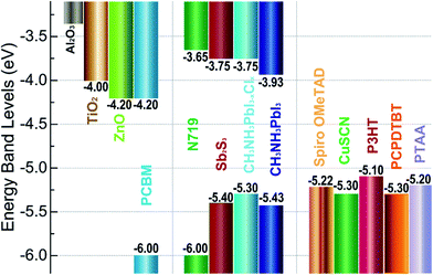 |
| | Fig. 5 Energy levels for some materials of ETL (left), absorbers (middle) and HTL (right) in solar cells. | |
3. Large-area (≥1 cm2) perovskite films fabricating technologies
The continuous fabrication of cracks- and pinholes-free the perovskite films and the selective carrier extraction layers films is difficulty for the large-area PSCs devices. So, some researchers have reported many fabrication methods to improve the quality of the large-area perovskite films.
3.1 Spin-coating and vacuum flash-assisted solution process (VASP)
Spin-coating has been widely used to fabricate the large-area perovskite films.16,35,39–41,45,91 The main advantage of the spin-coating method is to deposit thin films with well-defined the composition of chemical elements and the film thicknesses. Spin-coating includes one step spin-coating and two step spin-coating. One step spin-coating, briefly, methyl ammonium iodide (MAI) and lead iodide (PbI2) powders are mixed and dissolved in N,N-dimethylformamide (DMF) or dimethyl sulfoxide (DMSO), the mixed solution is spun on a TCO substrate and then annealed, attaining the perovskite films (Fig. 6). In 2015, M. Grätzel and L. Y. Han et al.41 prepared perovskite absorber films via one step spin-coating, they achieved large-area PSCs with an active area 1.02 cm2 that had a PCE > 15% (certified 15%). In 2016, W. Qiu and P. Heremans et al.39 achieved large-area PSCs with 4 cm2 aperture area and an active area of 1 cm2, that had a PCE of 13.6%.
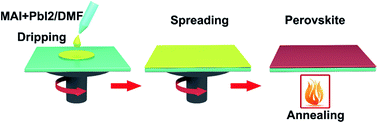 |
| | Fig. 6 One-step deposited perovskite films. | |
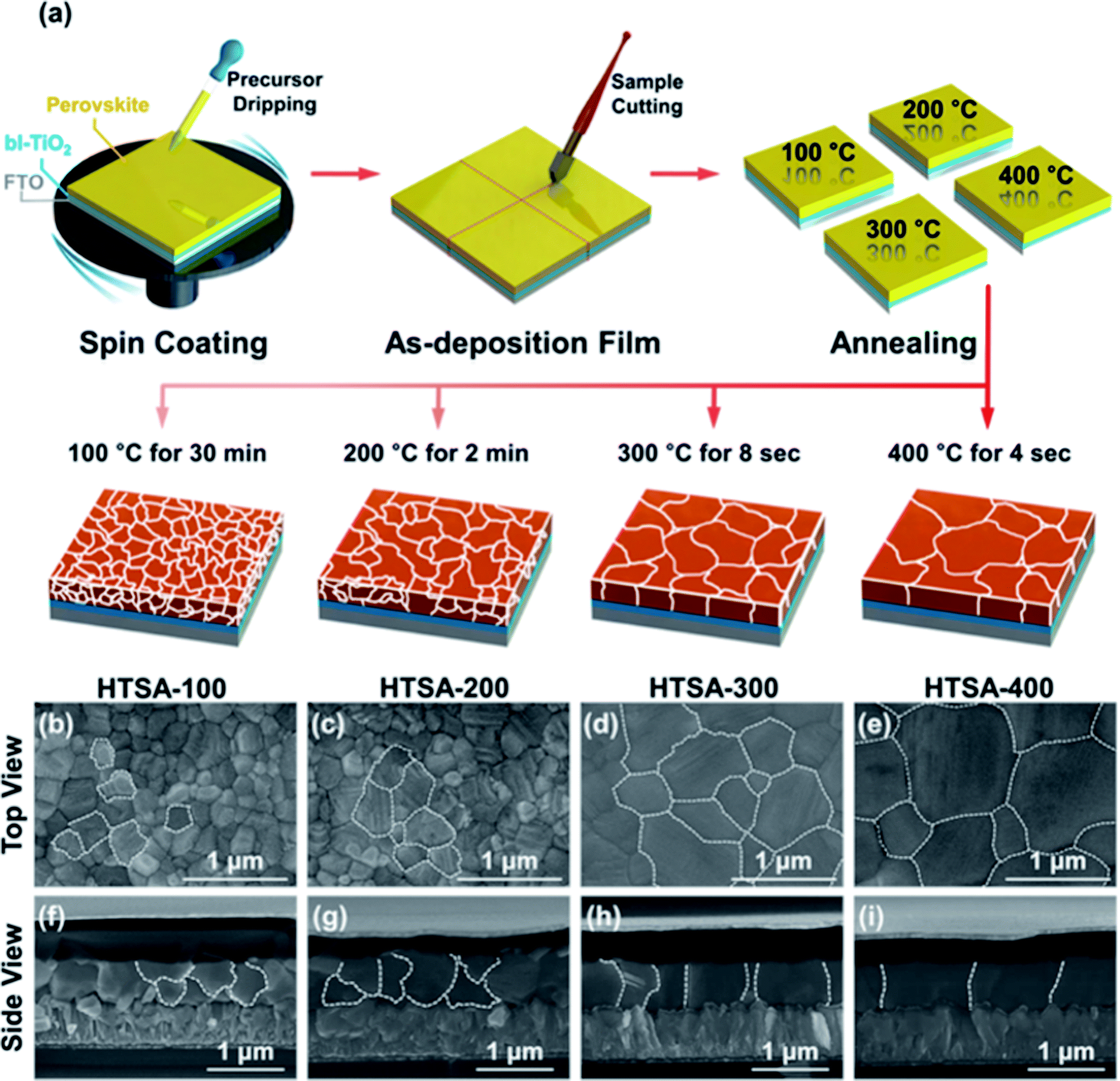
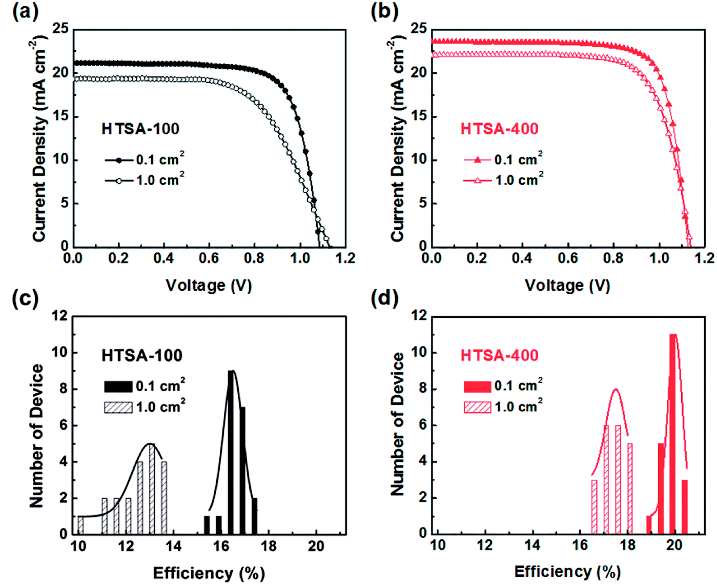
Aiming at uncovered pinhole areas derive from large perovskite grains, M. J. Kim and G. H. Kim et al.35 also developed one step spin-coating, and using high-temperature short-time annealing (HTSA) process (Fig. 7(a)), achieving the perovskite grains with sizes more than 1 μm without pinhole (Fig. 7(d, e, h, i)). In addition, the VASP was used to fabricate perovskite film (Fig. 8(a)), the sizes of perovskite grains were between 400 and 1000 nm (Fig. 8(c)), which covered the TiO2 layer.37
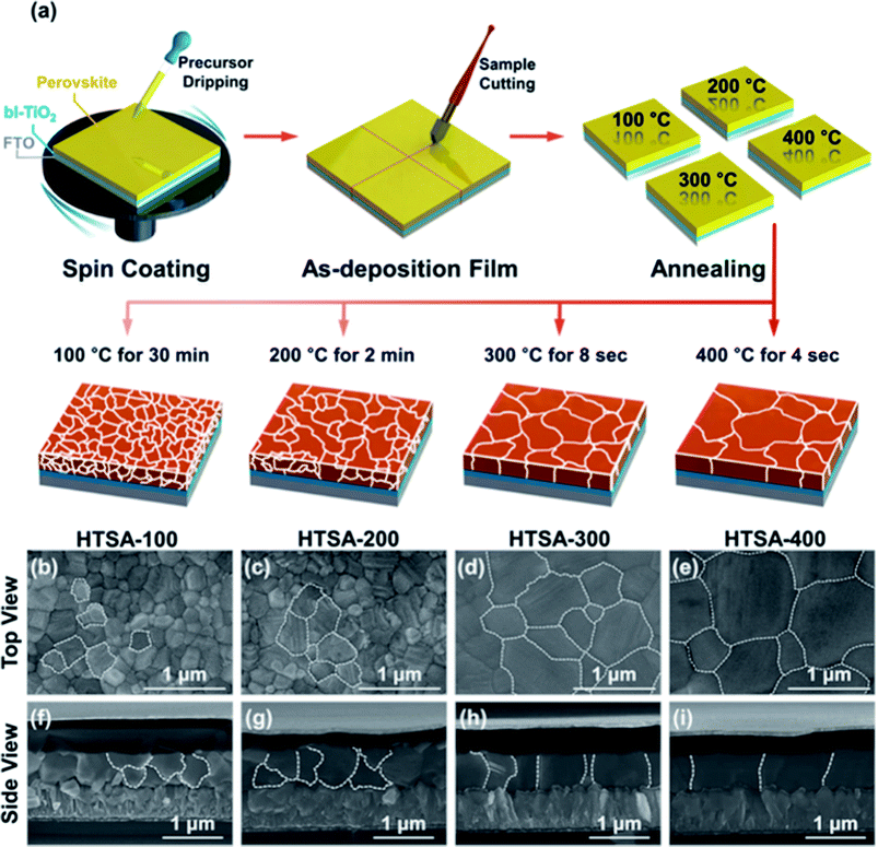 |
| | Fig. 7 (a) Schematic illustration of the annealing processes. (b–e) Surface SEM images (top view) of the perovskite films. (f–i) Their cross-sectional images (side view), respectively.35 | |
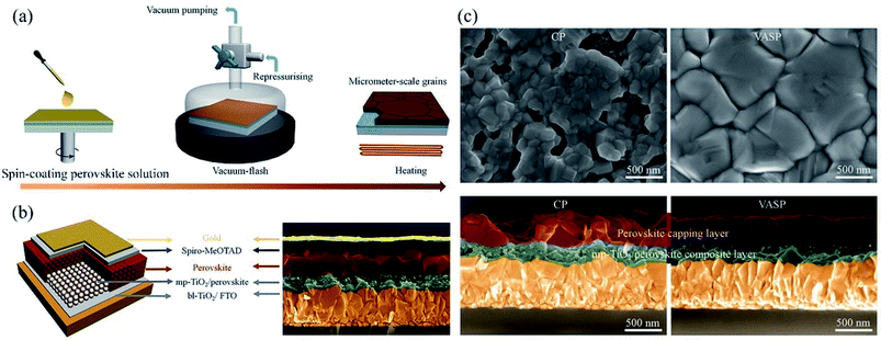 |
| | Fig. 8 (a) Schematic illustration of nucleation and crystallization procedures during the formation of perovskite film via VASP. (b) Schematic illustration of the PSCs configuration and SEM image. (c) Surface and cross-sectional SEM images of the perovskite films fabricated by the conventional process (CP) and VASP.37 | |
Two-step spin coating, briefly, MAI and PbI2 powders are dissolved in DMF or DMSO, respectively.16 First, the PbI2 solution is spun coating on a TCO substrate and then annealing, achieving the PbI2 films. Second, the MAI solution is spun coating on PbI2 films and then annealing, achieving the perovskite films (Fig. 9). In 2016, C. Chang et al.45 prepared perovskite absorber films with two step spin-coating, they achieved large-area PSCs with an active area 1.2 cm2 that had a PCE of 16.2%. In 2017, E. K. Kim, J. H. Noh and S. I. Seok et al.3 achieved large-area PSCs with an active area 1 cm2 that had a certified PCE of 19.7%. In 2017, X. W. Zhang and J. B. You et al.38 have adopted two-step spin-coating method to fabricate the (FAPbI3)1−x(MAPbBr3)x films and configure n–i–p planar structure PSCs with an active area 1 cm2 that has a PCE of 20.1%.
 |
| | Fig. 9 Two-step deposited perovskite films. | |
3.2 Vapor deposition
Comparing to the fabrication of the PSCs device with the spin-coating technology, vapor deposition technology offers a very superior device and superior performance (Fig. 10(a)). The vapor deposition includes dual-source evaporation technology,8 vapor–solid reaction,32 and vapor-assisted method,50 etc. For dual-source co-evaporation technology, it is that PbI2 powders and MAI powders are made as target source, and pre-heated to 116 °C and 325 °C, respectively, which has achieved the PSCs yield an PCE of 15.4%.8 This method fabricates high quality and uniformity of the perovskite films, subsequently resulting in good performance. But this method is very dependent on high temperature and high vacuum conditions. Alternate methods research in the literature32 is vapor–solid reaction (VSR), depositing the perovskite film with low temperature (Fig. 10(b)). First, the PbI2 film was spin-coated onto the ETL, and then baking on a 70 °C hot plate in air for 10 min. Second, MAI powders were dissolved in ethanol. Then the solution was homogeneously sprayed onto the bottom surface of the top plate that had been keeping at 80 °C. Finally, inside vacuum desiccator, two parallel hot plates (PHP) were putted together to synthesize perovskite thin films.32 H. Zhou and S. Yin et al.32 used this method to achieve the 8 × 8 cm2 PSCs module, the average PCE was 6.0% with the active area of 1.5 cm2.
 |
| | Fig. 10 (a) Schematic illustration of double source co-evaporation. (b) Schematic of vapor–solid reaction method.32 | |
3.3 Gas-induced method
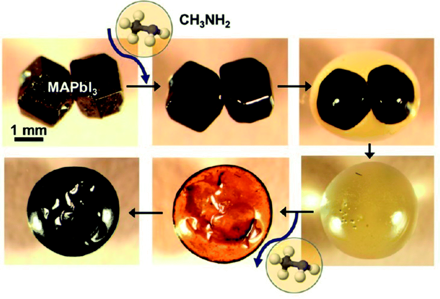
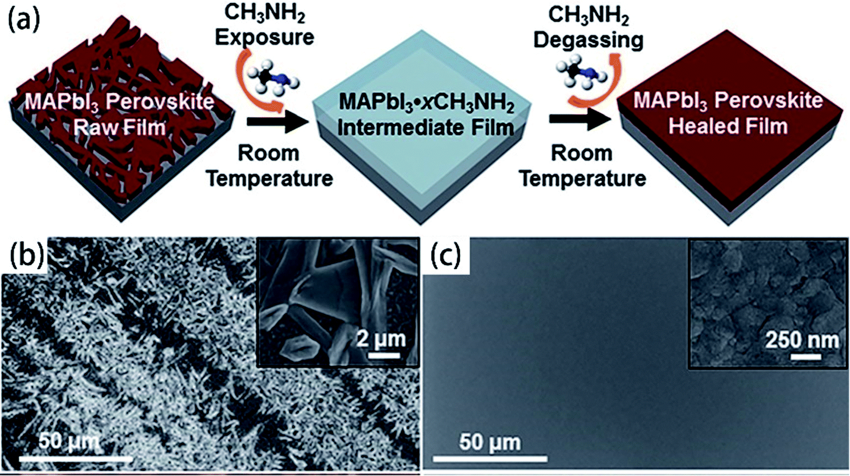
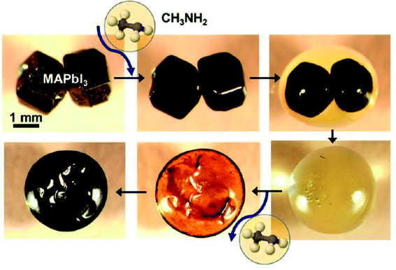
For the organic–inorganic halide perovskites (OIHPs) materials, gas-induce formation/transformation (GIFT) reveal surprising properties, such as gas-induced phase/morphology transformation.92 Z. Zhou, S. Pang, G. Cui et al.93 reported that the discovery of CH3NH2 (MA) induced phase/morphology transformation of the MAPbI3. As show in Fig. 11, MA gas is introduced at room temperature (RT), after 120 min, two MAPbI3 single-crystals become liquefied (MAPbI3·xCH3NH2), eventually, merge into one liquid sphere.93 Then MA gas is removed, after 120 min, perovskite back-conversion completed. Fig. 12(b) shows a poor quality of MAPbI3 thin film (incomplete coverage, rough), then the MA gas treatment has been introduced to create smooth, uniform and full coverage MAPbI3 thin films (Fig. 12(c)).93
 |
| | Fig. 11 In situ optical microscopy of the morphology evolution of two touching MAPbI3 perovskite crystals (same magnification) upon exposure to CH3NH2 gas and CH3NH2 degassing.93 | |
 |
| | Fig. 12 (a) Schematic illustration of MA induced defect-healing of MAPbI3 perovskite thin films. SEM images of MAPbI3 thin films: (b) raw film and (c) healed film.93 | |
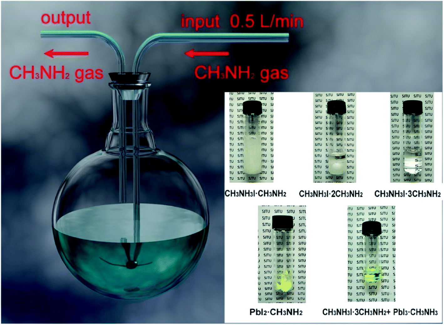
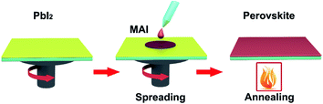
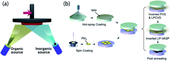
In 2017, M. Grätzel and L. Han et al.36 achieved 8 × 8 cm2 perovskite films via GIFT, briefly, at atmospheric environment, dried CH3NH2 gas (0.5 l min−1) was passed into a bottle that contained 2 mmol CH3NH3I or PbI2 powders (Fig. 13). After 30 min, the CH3NH3I powders changed into transparent colorless liquid (CH3NH2I·3CH3NH2), and the PbI2 powders changed into a pale-yellow paste (PbI2·CH3NH2, Fig. 13).36 For the synthesis of perovskite precursor, CH3NH2I·3CH3NH2 and PbI2·CH3NH2 were blended stoichiometrically and ultrasonicated for 15 min (Fig. 13).36 The perovskite precursor (200 μl) was dropped on a 8 × 8 cm2 substrate and then the precursor was covered by the polyimide (PI) film.36 A pressure of 120 bar was loaded via a pneumatically driven squeezing board which spread the liquid precursor under the PI film. The pressure was held for 60 s and then unloaded. The thin liquid film covered with the PI film was heated at 50 °C for 2 min before peeling off the PI film. After peeling the PI film (50 mm s−1), a dense and uniform perovskite film was formed (Fig. 14(b)).36 They achieved the PSCs with the device area 36 cm2 (Fig. 14(c)) that had a certified PCE of 12.1%.36
 |
| | Fig. 13 Diagram of the CH3NH2 introduced CH3NH3I and PbI2 powers and the mixture of CH3NH3I·3CH3NH2 and PbI2·CH3NH2.36 | |
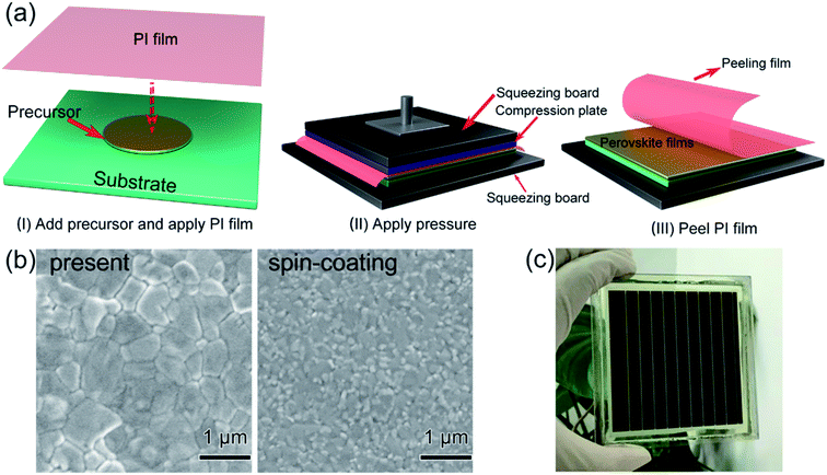 |
| | Fig. 14 Diagram of the pressure processing method for the deposition of perovskite films. (a) The steps of the pressure processing method. (b) SEM images. (c) Photograph of a perovskite module.36 | |
3.4 Other approaches
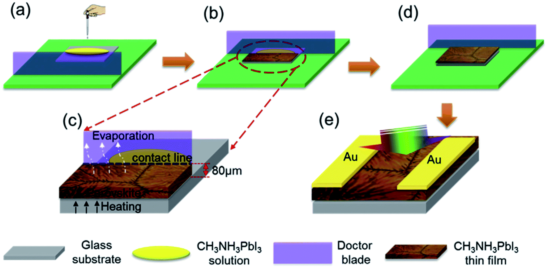
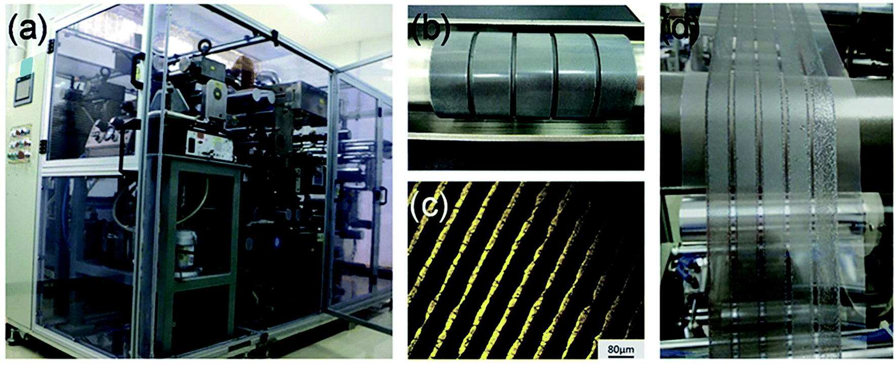
In addition, a blade coating technology is also frequently used, the schematic shows in Fig. 15.22 The advantage of the blade coating technology can control the distance between blade and the substrate, and the in situ thermal-treatment temperature. In 2015, S. Razza and A. D. Carlo et al.47 used the blade coating technology, which achieved a module PSCs with a 10.1 cm2 active area that had the efficiency of 10.4%.47 Meanwhile, an efficiency of 4.3% had been measured for a module area of 100 cm2.47 In 2016, J. L. Yang et al.94 reported an approach to fabricate ultra-long nanowires array and highly oriented CH3NH3PbI3 thin films in ambient environments, briefly, this approach included large-scale roll-to-roll micro-gravure printing and doctor blading (Fig. 16), which produced perovskite nanowires lengths as long as 15 mm.94
 |
| | Fig. 15 Schematic representation of in situ doctor blading technology for fabricating CH3NH3PbI3 films.22 | |
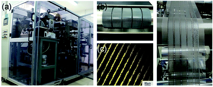 |
| | Fig. 16 (a) Photo of self-developed R2R multi-function printer. (b) Photo of micro-gravure printer roller. (c) Optical microscope image of engraved micro-gravure printer roller. (d) A photo of R2R printing process.94 | |
4. Methods of improving PCE for large-area (≥1 cm2) perovskite solar cells
For the large-area PSCs device, improving the PCE, the first method is to change the chemical composition of perovskite, adjusting its band gap and increasing the charge generation.3,29,31,35,38,46 The second approach is to increase the grain size of perovskite, decreasing the cracks and pinholes, that reduces the bulk defect recombination and electric leakage, and increase Voc.35–38 The third approach is interface modification, which reduces interface contact resistance, and reduce interface and surface recombination, and increase Jsc.31,41,45,95
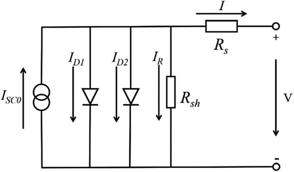
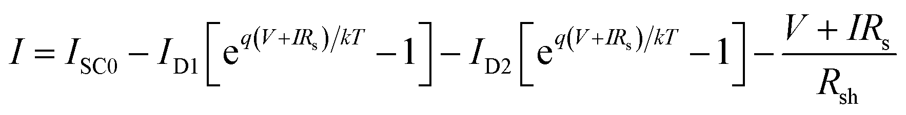
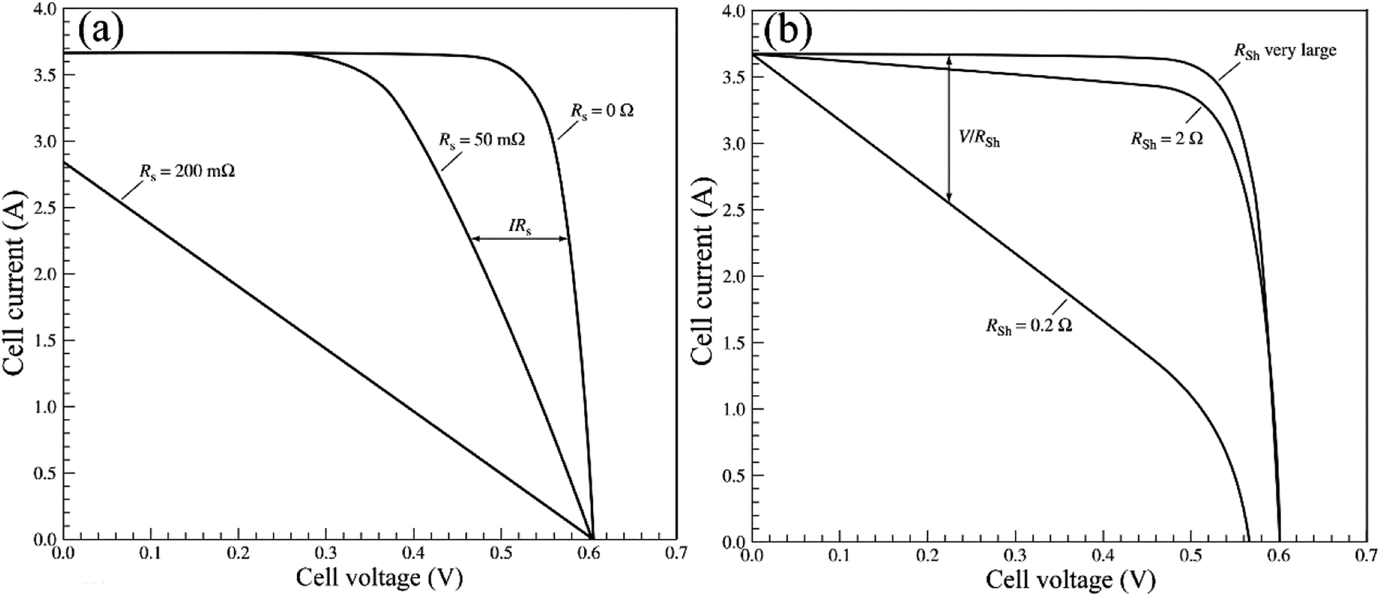
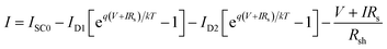
For the large-area PSCs device, with the increasing of cell size, the series resistance (Rs) increase among the charge transfer layers, the absorber layer and the electrode layers. At the same time, the number of the crack and the pinholes increase, that from the shunt resistance (Rsh) and the value of Rsh decrease. Incorporating these resistances into the circuit model of the solar cells device shows in Fig. 17.96 The increasing of Rs and the decreasing of Rsh increase the interface losses of the large-area PSCs device, that is the major reason of the lower efficiency for the large-area PSCs device.95
 |
| | Fig. 17 Incorporating these resistances into the circuit model.96 | |
The current expression in the circuit can be written as eqn (2).96
| |
 | (2) |
where
ISC0 is the short-circuit current when there are no parasitic resistances (
Rs and
Rsh). The effect of these parasitic resistances on the
I–
V characteristic is shown in
Fig. 18. Form the
eqn (2), the series resistance,
Rs increase, has no effect on the open-circuit voltage, but reduces the short-circuit current (
Jsc) and fill factor (FF) (
Fig. 18(a)). Conversely, the shunt resistance,
Rsh decrease, has no effect on the short circuit current, but reduces the open-circuit voltage (
Voc) and FF (
Fig. 18(b)).
 |
| | Fig. 18 (a) I–V curve of Rs, (b) I–V curve of Rsh.96 | |
4.1 Chemical molecular engineering
For the perovskite material, its band gap can regulate via exchange the chemical molecular or element, achieving an ideal band gap of the perovskite material. Such as, through intramolecular exchange, formamidinium (FA) molecular is frequently used to replace methylamine (MA) in MAPbI3, forming FAPbI3 and adjusting the band gap. In 2015, W. S. Yang and J. H. Noh et al.29 have fabricated FAPbI3 films, its band gap is 1.47 eV smaller than MAPbI3 (1.50 eV). Meanwhile, the PCE of FAPbI3-based PSCs is up to 20.1%. In 2017, J. Y. Kim and D. S. Kim et al.35 fabricated (FAPbI3)0.85(MAPbBr3)0.15 (1.55 eV) as absorber layer of the PSCs device, which had a maximum PCE exceeding 18% over a 1 cm2 active area. In 2017, E. K. Kim, J. H. Noh and S. I. Seok et al.3 introduced additional iodide ions into the organic cation solution, that decreased the concentration of deep-level defects. They fabricated of the (FAPbI3)x(MAPbBr3)1−x-based PSCs with a certified PCE of 19.7% in 1 cm2 cells.3 Adding inorganic cesium to triple-cation perovskite compositions, E. H. Sargent et al.31 have reported the best-performance large-area (1.1 cm2) PSCs (Cs0.05FA0.81MA0.14PbI2.55Br0.45, 1.60 eV), that has a PCE of 20.3%. In 2017, X. W. Zhang and J. B. You et al.38 used the (FAPbI3)1−x(MAPbBr3)x (1.55 eV) as absorber layer for PSCs with the certified efficiency of 20.1% in large-area (1 cm2).38
4.2 Improving preparation technology
The high quality (cracks- and pinholes-free) large-area perovskite film is precondition for the achieving high PCE of PSCs. Because the cracks and pinholes can form electric leakage (forming the Rsh), which lead to the decreasing the Voc and FF, and reduce the PCE of PSCs. So, M. J. Kim and G. H. Kim et al.35 developed one step spin-coating, and using high-temperature short-time annealing process (Fig. 7(a)), achieving the perovskite grains with sizes more than 1 μm without pinhole (HTSA-400, Fig. 7(d, e, h and i)). They fabricated PSCs device with 1 cm2, which achieved the PCE of 18.32% with HTSA-400 (Fig. 19(d)), but the PCE is only 13.82% with HTSA-100 (Fig. 19(c)).35 X. Li and M. Grätzel et al.37 used the vacuum flash-assisted solution processing (VASP) to fabricate perovskite film (Fig. 8(a)), the sizes of perovskite grains were between 400 and 1000 nm (Fig. 8(c)). They fabricated the PSCs device with an aperture area exceeding 1 cm2, the certified PCE of 19.6%.37 In 2015, Z. Zhou, S. Pang, G. Cui et al.93 reported that the MA gas treatment has been introduced to create smooth, uniform and full coverage MAPbI3 thin films (Fig. 12(c)).93 This MAPbI3 was used to fabricate the PSCs device, the PCE increased from 5.7% to 15.1%, was observed, which was clearly the result of the improving film morphology.93
 |
| | Fig. 19 (a) Current−voltage curves of perovskite solar cells derived from HTSA-100 and (b) HTSA-400 with an active area 0.1 cm2 and a 1 cm2. (c) Histogram of PCEs derived from HTSA-100 and (d) HTSA-400 with an active area 0.1 cm2 and 1 cm2.35 | |
4.3 Interface engineering
Interface engineering can optimize interface contact, mitigate carrier recombination and increase carrier collection, which is extremely important to achieve high-performance and high-stability PSCs. Interface engineering includes doped, plasma etching, self-assembled monolayers and interface buffer layer etc.
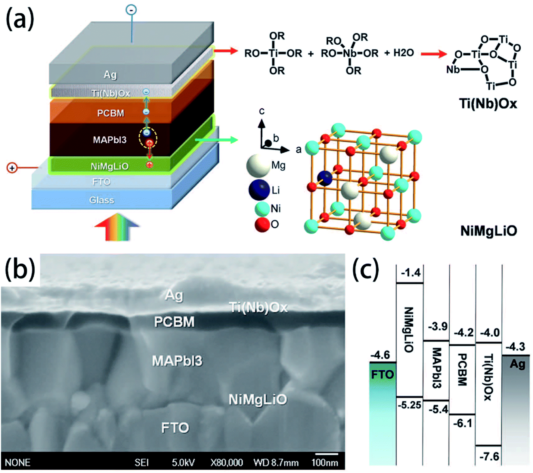
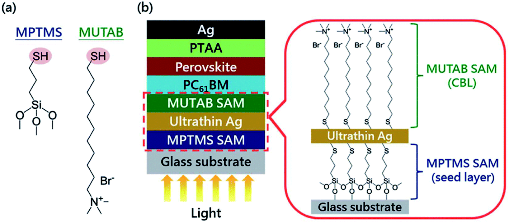
Doping for the charge transport layers, that can improve their electrical performance, such as improving carrier concentration and mobility. For Li–Mg co-doped NiO films, the conductivity is 2.32 × 10⁻³ S cm−1, ∼12 times greater than that of the pure MgxNi1−xO.41 The conductivity of Nb5+ doped TiO2 films is ∼104 S cm−1, ∼100 to 1000 times greater than that of the pure TiO2.41 In 2015, M. Grätzel and L. Y. Han et al.41 have used Mg–Li co-doped NiO as HTL and Nb doped TiOx as ETL material in inverted planar PSCs to achieve very rapid carrier extraction, increasing the cell FF from 0.64 to 0.827. Meanwhile, they fabricated a large-area (>1 cm2) PSCs (Fig. 20(a)) with a certified efficiency of 15%.41 The contact-passivation can mitigate interfacial recombination and improve interface binding in low-temperature planar PSCs. H. R. Tan and E. H. Sargent et al.31 reported a contact-passivation strategy using chlorine-capped TiO2 (Cl–TiO2) colloidal nanocrystal film as ETL, the charge-recombination lifetime increased from 64 μs to 145 μs compare with pure TiO2 film.31 They fabricated the planar PSCs for active areas of 1.1 cm2, that achieved a certified efficiency of 19.5% without hysteresis.31 Interlayers are thin layers or monolayers of organic molecules that modify a specific interface in the solar cell.97 In 2016, C.Y. Chang and Y. C. Chang et al.45 reported an approach for the modification of interface layer via introducing thiol-functionalized self-assembled monolayers (SAMs, Fig. 21(b)), which decreased interface charge recombination and increased the value of Jsc (19.43 mA cm−2 to 21.68 mA cm−2) and FF (0.67 to 0.72). They fabricated a large-area (1.2 cm2) PSCs with the PCE up to 15.98%.45 Y. Wu and X. Yang et al.42 reported a perovskite–fullerene graded heterojunction structure, which improved the photoelectron collection and reduced recombination loss. They fabricated the PSCs of 1.022 cm2, that had a certified PCE of 18.21%.42
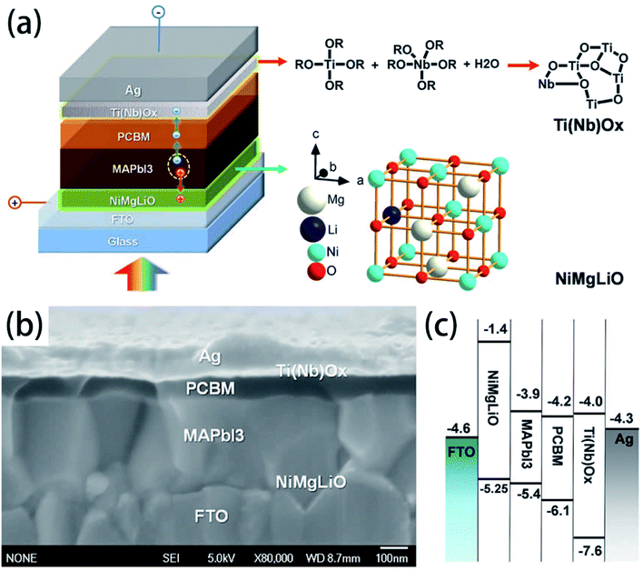 |
| | Fig. 20 Structure and band alignments of the PSCs, (a) diagram of the cell configuration highlighting the doped charge carrier extraction layers. (b) A high-resolution cross-sectional SEM image of a complete solar cell. (c) Band alignments of the solar cell.41 | |
 |
| | Fig. 21 (a) Chemical structures of SAM molecules. (b) Schematic illustration of the device architecture used in this study.45 | |
5. Stability of large-area (≥1 cm2) perovskite solar cells
In recent years, the certificated PCE of the large-area (1 cm2) PSCs has achieved 20.1%.38 However, the major issue of large-area PSCs for commercial applications is the poor long-term device stability. For the stability of the perovskite materials and devices, it is necessary to consider the effects of temperature, illumination and ambient (oxygen, moisture) exposure. Many papers have reported about this important issue.1,51,53,97–107
5.1 Degradation mechanisms
The degradation of the PSCs device includes the degradation of the active layer, the degradation of charge transport layers, and the degradation of electrodes.104 The MAPI3 films are frequently used as absorber layer film. But the major problem with MAPbI3 is that has thermal decomposition (exceeding 85 °C)108,109 and water decomposition.1,48,110 Some researchers have reported the decomposition process of MAPbI3. B. Philippe and H. Rensmo et al.109 exposed the MAPbI3 and MAPbI3−xClx to various environments. From the photoelectron spectroscopy results with the different environments, the perovskite has decomposed into PbI2, but this degradation seems to occur already at 100 °C and is not only related to large humidity (Fig. 22(a)). Meanwhile, they observed a slow degradation occurs even when stored in an inert atmosphere such as argon.109 L. D. Wang et al.48 verified that oxygen, together with moisture, could lead to the irreversible degradation of MAPbI3. They exposed TiO2/CH3NH3PbI3 film to air with a humidity of 60% at 35 °C for 18 h, and then, the absorption between 530 and 800 nm greatly decreased (Fig. 22(b)), the MAPbI3 decomposed into PbI2 and I2 (Fig. 21(c)).48 The degradation mechanism of MAPbI3 upon exposure to moisture in absence of illumination involves the formation of hydrate form, which can be reversible.11,48,111,112 However, continuing exposure to moisture and/or exposure to illumination leads to the irreversible degradation to PbI2.111 For ETL material, TiO2 is especially sensitive to ultraviolet light, in the ultraviolet light, Ti4+ adsorb O2 and convert into Ti3+, increasing the charge recombination.113 Meanwhile, the lithium salt in spiro-MeOTAD is easy to absorb moisture and decrease the PSCs device stability.
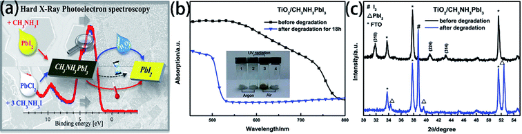 |
| | Fig. 22 (a) Degradation of MAPbI3 in moisture and air atmosphere.109 (b) UV-vis absorption spectra of TiO2/MAPbI3 film before and after degradation.48 (c) XRD patterns of TiO2/MAPbI3 film before and after degradation.48 | |
5.2 Methods of improving stability
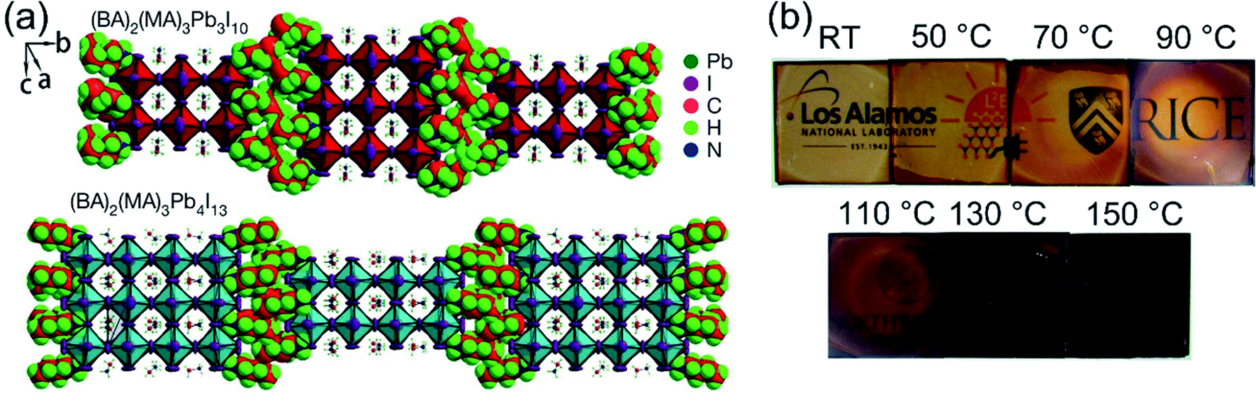
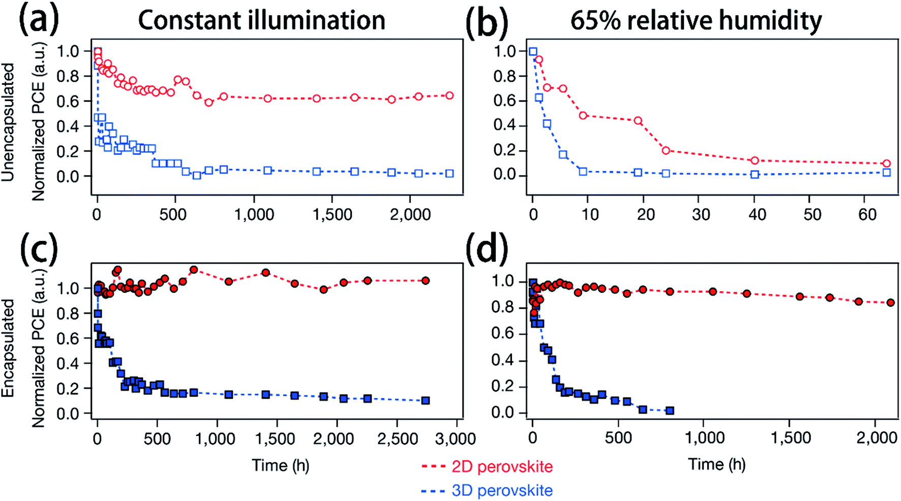
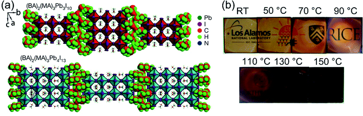
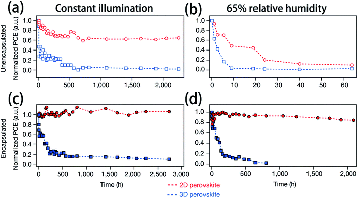
In recent years, many methods have been researched to improve the PSCs device stability. Due to the poor stability of MAPI3, the first method is to modify the chemical constituents or structure of the perovskite. For example, 2D perovskites, compared with 3D perovskites, 2D perovskites have the higher carrier mobility while maintaining good ambient stability.114,115 The 2D Ruddlesden–Popper layered perovskites ((BA)2(MA)2Pb3I10 and (BA)2(MA)3Pb4I13) have been studied (Fig. 23(a)).115 The (BA)2(MA)3Pb4I13 film color gets darker with increasing temperature (Fig. 23(b)).115 H. Tsai and W. Nie et al.115 have achieved a PCE of 12.51% with 2D (BA)2(MA)3Pb4I13 PSCs device. Under the constant light illumination, after 2500 h, the 2D perovskite devices is retaining 70% of its original PCE without encapsulated and 98% with encapsulated. The 3D perovskite devices have degraded < 10% of its original PCE after 2500 h (Fig. 24(a and c)). Fig. 24(b) shows the PCE of the unencapsulated 2D and 3D devices, that shows degradation after 60 h, under 65% relative humidity.115 With simple encapsulation, after 2500 h, the 2D devices retained 80% of its original PCE under 65% relative humidity, but the 3D devices had been degraded (Fig. 24(d)).115 K. Yao et al.46 used the polyethylenimine (PEI) cations to fabricate the 2D perovskite compounds (PEI)2(MA)n−1PbnI3n+1 (n = 3, 5, 7), which was used as absorber layer to fabricate PSCs with an aperture area of 2.32 cm2 under ambient humidity that have a PCE up to 8.77%. After 500 h, the PCE of the 2D large-area PSCs device only decreased by ∼5%.46
 |
| | Fig. 23 Crystal structure and thin-film characterization of layered perovskites. (a) The crystal structure of the Ruddlesden–Popper (BA)2(MA)2Pb3I10 and (BA)2(MA)3Pb4I13 layered perovskites. (b) Photos of (BA)2(MA)3Pb4I13 thin films cast from room temperature (RT) to 150 °C.115 | |
 |
| | Fig. 24 (a and c) Photostability tests under constant AM1.5G illumination for 2D ((BA)2(MA)3Pb4I13; red) and 3D (MAPbI3; blue) perovskite devices. (b and d) Humidity stability tests under 65% relative humidity at in a humidity chamber for 2D ((BA)2(MA)3Pb4I13; red) and 3D (MAPbI3; blue) perovskite devices.115 | |
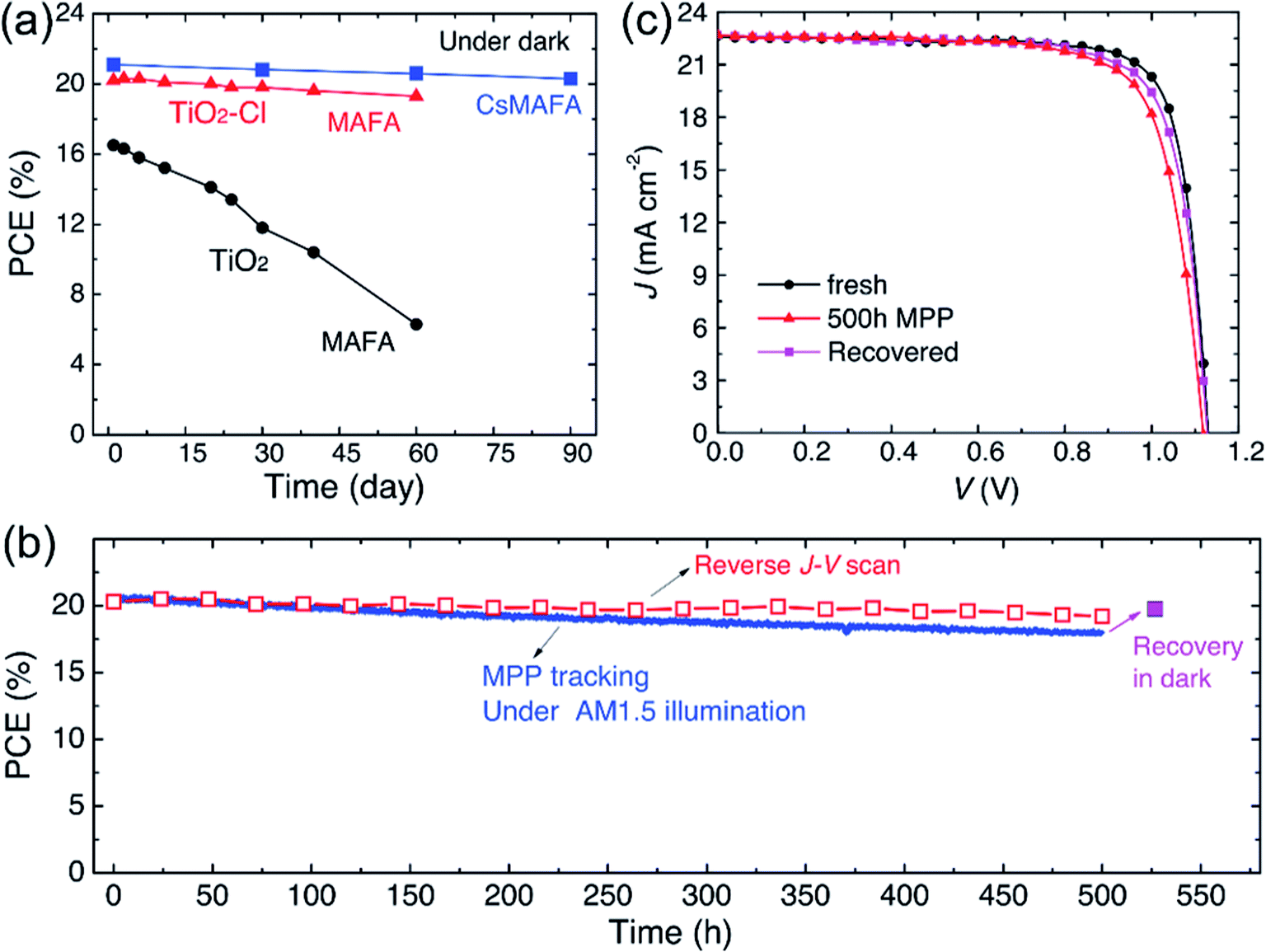
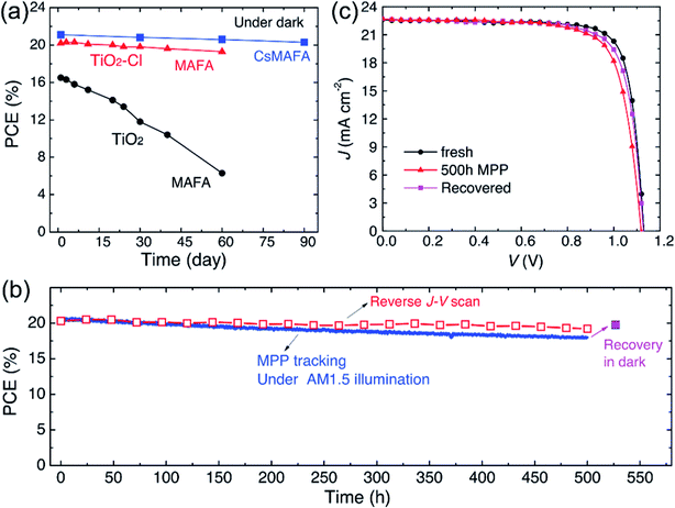
Furthermore, the alkali metal cation is introduced into the perovskite material, which can improve the stability of the PSCs device.31,68,116 E. H. Sargent et al.31 added cesium cation to fabricate a triple-cation perovskite compositions films (Cs0.05FA0.81MA0.14PbI2.55Br0.45), that was made the large-area (1.1 cm2) PSCs with a PCE up to 20.3% (Fig. 25(b and c)). After 90 days, the PSCs devices retained 96% of its initial PCE (Fig. 25(a)).31 Rubidium (Rb) cations can stabilize the black phase of FA perovskite and be integrated into PSCs, M. Saliba and M. Grätzel et al.116 have used RbCsMAFAPbI3 as absorber layer of the PSCs device. After 500 h at 85 °C under continuous illumination, the device has retained 95% of its initial PCE (Fig. 26(d)).116
 |
| | Fig. 25 Long-term device stability of PSCs with TiO2–Cl and TiO2. (a) Dark storage stability of non-encapsulated PSCs. (b) Continuous maximum power point tracking for 500 hours of a high performance unsealed CsMAFA cell with TiO2–Cl in nitrogen atmosphere under constant simulated solar illumination. (c) J–V curves of the PSCs (CsMAFA) from (b) at various stages.31 | |
 |
| | Fig. 26 (a) J–V curve of RbCsMAFA solar cell. (b) J–V curve of the highest-Voc device. (c) EQE electroluminescence (EL) as a function of voltage. (d) Thermal stability test of a perovskite solar cell.116 | |
The second method for improving the PSCs device stability is to modify the charge transport layer (ETL and HTL), or use the new type charge transport material.61 Because TiO2 is especially sensitive to ultraviolet light,113 some new ETL materials have been reported. A. D. Carlo et al.117 reported an additional lithium-neutralized graphene oxide (GO-Li) layer as interface layer was inserted between TiO2 ETL and perovskite layer, that improved the stability of PSCs devices.117 A. Hagfeldt et al.118 has used ZnO nanorod arrays as ETL replace the TiO2, achieving the PSCs device, it has been exposed in atmospheric environment without encapsulation, and maintaining 90% of the original efficiency. X. W. Zhang and J. B. You et al.57 have used SnO2 as ETL for planar-structure PSCs, it is found that the devices can maintain almost their original efficiency when store in dry air conditions for 40 days.57 J. H. Noh and S. I. Seok et al.66 used La-doped BaSnO3 as ETL, the PSCs retained 93.3% of its initial PCE after 1000 hours, whereas the TiO2 cells had completely degraded within 500 hours.
For the HTL materials, spiro-OMeTAD is the most commonly used HTL material,35,57,67 the certified PCE of 22.1% in small cell.3 But the lithium salt in spiro-MeOTAD is easy to absorb moisture and reduce the PSCs device stability. So inorganic and hydrophobic hole transport material are used to improve the PSCs device stability.41,54,74,78,79 M. Grätzel and L. Y. Han et al.41 used Li0.05Mg0.15Ni0.8O as HTL material and Ti(Nb)Ox as ETL to fabricate inverted planar heterojunction structure device (p–i–n), under simulated solar light, the PSCs device maintained 90% of the original efficiency after 1000 h. S. H. Yang et al.79 has fabricated inverted planar heterojunction structure for NiO-based PSCs device (p–i–n), achieving more than 85% of its original PCE has been kept after 150 days. Z. B. He et al.78 used NiOx nanocrystal as HTL in planar PSCs device. After 1000 h, the PCE of PSCs device maintained 87% of its initial value. N. Arora and M. Grätzel et al.74 used one new HTL material CuSCN. They achieved the PSCs with PCE > 20%, after 1000 hours at 60 °C, the PSCs devices retained >95% of their initial efficiency. CuGaO2 as HTL in n–i–p configuration PSCs, exposing it directly to the ambient environment without encapsulation. After 30 days, it maintains 87% its initial PCE.54
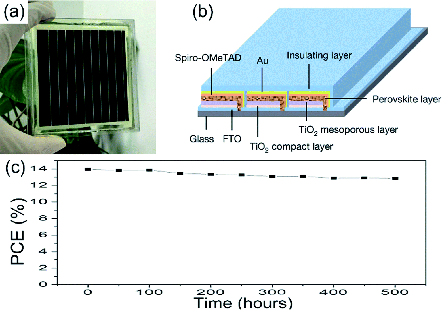
Other methods for improving the PSCs device stability include the PSCs structure optimization, interface optimization, encapsulation, etc.81,82,119 A hole-conductor-free structure of the PSCs can achieve long-term stability. Exposing the PSCs device (c-TiO2/m-TiO2/ZrO2/carbon) under full AM 1.5 simulated sunlight over 1008 hours, the PCE maintains 100% of its initial value.82 To improve the stability of the device, the insulation material encapsulate the PSCs device is frequently used. M. Grätzel and L. Y. Han et al.36 encapsulated the large-area PSCs device (36.1 cm2, TiO2 ETL, Fig. 27(a and b)) by the insulation material, the module retained 90% of its initial performance after 500 h (Fig. 27(c)).
 |
| | Fig. 27 Illustration of the perovskite module and device performance. (a) Photograph of a module. (b) Diagram of the module structure. (c) Evolution of the photovoltaic stability of an encapsulated perovskite solar module.36 | |
6. Other issues
6.1 Cost analysis
For conventional solar PV technology, it need high energy and vacuum to process solar cells. Thus, these PSCs can turn-out to be a promising solution in replacing the conventional PV technology. In this section, we briefly analyze the cost for various raw materials of a 1 m2 PSCs module. Conventional PSCs device architecture is shown in Fig. 4(a), that include glass substrate, TCO (FTO), ETL (TiO2), perovskite absorber layer (MAPbI3), HTL (spiro-OMeTAD) and metal electrode (Au). For 1 m2 conventional PSCs module, raw material utilization for cleaning, deposition of various layers and encapsulation of the module were extracted from various available literature sources and their corresponding data are included in Table 3.120,121 From the data (Table 3), it is clear that about 43% of the total raw material cost is from FTO substrate, about 34% from the HTL material (spiro-OMeTAD), and 18% from metal electrode (Au).120,121
Table 3 Cost breakdown of raw materials utilized in fabricating a PSC module of 1 m2 with 70% active area120,121
| Raw material |
Qty |
Price (in USD) |
Contribution towards total cost (%) |
Comments |
| FTO glass |
1 m2 |
766 |
43.0500 |
Processing cost of FTO is included |
| Ethanol |
32.84 ml |
4.59 |
| DI water |
32.70 ml |
0.002 |
| HCL solution |
4.66 ml |
1.8204 |
![[thin space (1/6-em)]](https://www.rsc.org/images/entities/char_2009.gif) |
| Blocking layer |
| TAA |
19.16 ml |
7.339 |
0.0066 |
For 100 nm layer and post deposition cleaning is included |
| Ethanol |
32.84 ml |
4.59 |
| DI water |
32.70 ml |
0.002 |
|
| ETL material |
| TiO2 |
49.5 g |
41.12 |
0.02291 |
For 250 nm thick layer |
|
| Perovskite layer |
| PbI2 |
1.38 g |
4.26 |
0.003811 |
For 100 nm thick solvent PbI2 followed by 200 nm thick solvent MAI |
| DMF |
2.98 ml |
0.5502 |
| MAI |
0.143 g |
0.49 |
| IPA |
14.29 ml |
1.538 |
|
| HTL material |
| Spiro-OMeTAD |
0.850 g |
603.65 |
33.973 |
For 200 nm thick solvent HTM layer |
| Chlorobenzene |
10.67 ml |
5.9 |
|
| Cathode |
| Au |
1.65 g |
330 |
18.392 |
For 100 nm thick layer |
|
| Encapsulation |
| 3 M tape |
|
22.32 |
0.012 |
Taped on both sides |
| PET |
61.7 g |
0.03 |
These data suggest the need for replacement of conventional FTO substrate, HTL material and Au electrode. The efficiency of the PSCs device on ITO-free analogues achieved 11%.122 Some new and cheap HTL materials have been reported, such as NiO (PCE ∼ 18.47%),79 triazine-Th-OMeTPA (PCE ∼ 12.51%),75 CuGaO2 (PCE ∼ 18.51%),54 CuSCN (PCE ∼ 20.4%),74 NiMgLiO (PCE ∼ 16.2%),41 etc. Meanwhile, the efficiency for carbon based HTM-free PSCs devices achieved 15.9%.81 Although, the PCE of spiro-OMeTAD-free PSCs device is little lower than the conventional PSCs, with small sacrifice in efficiency, low-cost and highly stable carbon based HTM-free PSCs can be fabricated.
6.2 Environmental issues – the presence of lead
Environmental issues are a well-recognized issue for PSCs.104,123 Like CdTe, a toxic heavy metal exists in the PSCs devices. But, the CdTe is very chemically stable, organolead halide perovskites are not stable and upon ambient exposure they can degrade into products that are readily leached into the environment.104,123 In the life cycle assessments (LCA), the hazards of Pb for environmental impacts exist in all stages, which include raw material extraction, synthesis of starting products, fabrication, use and decommissioning.120 Thus, ideally PSCs should be subject to even more stringent safety standards and any commercial products should have clear plans for end-of-life disposal and/or recycling.104,123
To address the concerns about lead, lead-free perovskite materials have attracted the attention of many researchers, which include tin-based perovskite materials and other perovskites materials (lead-free and tin-free perovskites, such as MA2CuClxBr4−x,124 CsGeI3, MAGeI3, and FAGeI3,125 A3Sb2I9 (A = Cs, Rb),126 Cs2BiAgCl6,127 (N-methylpyrrolidinium)3Sb2Br9,128 etc.). But, compare with lead-based perovskites, the efficiencies of tin-based PSCs commonly well below 10%,129,130 the PCE values for other perovskites have been below 1%.124–126
Thus, improving encapsulation technologies, it could limit the Pb leakage during the cell operation. Researching the lead-free perovskite materials, achieving high performance lead-free PSCs device, which could to replace the lead-based PSCs device.
7. Conclusions
In this article, we briefly summarized the studies on large-area PSCs in recent years. Progress has been made in manufacturing larger area cells as well as modules, which is the interesting for commercialization of the technology. Approaches for fabricating the lager-area perovskite film layer are described such as spin-coating, vapor deposition, gas-induced and blade coating etc. It is demonstrated that these processes are useful to realize more uniform perovskite layer with larger grain sized and better surface coverage, which strongly affect consequent photovoltaic performance of devices.
Going forward, PSCs will have to reduce non-radiative recombination and improve charge transport in order to achieve the highest possible Voc values and fill factors. For the large-area PSCs device, improving the PCE, the first method is to change the chemical composition of perovskite, adjusting its band gap and increasing the charge generation. The second approach is to increase the grain size of perovskite, decreasing the cracks and pinholes, that reduces the bulk defect recombination and electric leakage, and increase Voc. The third approach is interface modification, which reduces interface contact resistance, and reduce interface and surface recombination, and increase Jsc. Meanwhile, one key issue of the large-area PSCs is the long-term poor stability. To the improving of the stability of PSCs, which requires interdisciplinary research to find new stable materials, the choice of electrodes, barrier layers, charge transport layers and encapsulation strategies. Undoubtedly, in the near future, halide perovskite materials have emerged as an attractive alternative to conventional silicon solar cells.
Conflicts of interest
The authors declare that there is no conflict of interests regarding the publication of this paper.
Acknowledgements
This project was supported by National Science Foundation of China (NSFC No. 61574009 and No. 11574014).
References
- H. Tang, S. He and C. Peng, Nanoscale Res. Lett., 2017, 12, 410 CrossRef PubMed.
- M. K. Nazeeruddin, Nature, 2016, 538, 463–464 CrossRef PubMed.
- W. S. Yang, B. W. Park, E. H. Jung, N. J. Jeon, Y. C. Kim, D. U. Lee, S. S. Shin, J. Seo, E. K. Kim, J. H. Noh and S. I. Seok, Science, 2017, 356, 1376 CrossRef CAS PubMed.
- S. De Wolf, J. Holovsky, S. J. Moon, P. Loper, B. Niesen, M. Ledinsky, F. J. Haug, J. H. Yum and C. Ballif, J. Phys. Chem. Lett., 2014, 5, 1035–1039 CrossRef CAS PubMed.
- S. D. Stranks, G. E. Eperon, G. Grancini, C. Menelaou, M. J. Alcocer, T. Leijtens, L. M. Herz, A. Petrozza and H. J. Snaith, Science, 2013, 342, 341 CrossRef CAS PubMed.
- A. Kojima, K. Teshima, Y. Shirai and T. Miyasaka, J. Am. Chem. Soc., 2009, 131, 6050 CrossRef CAS PubMed.
- L. Etgar, P. Gao, Z. Xue, Q. Peng, A. K. Chandiran, B. Liu, M. K. Nazeeruddin and M. Grätzel, J. Am. Chem. Soc., 2012, 134, 17396–17399 CrossRef CAS PubMed.
- M. Liu, M. B. Johnston and H. J. Snaith, Nature, 2013, 501, 395–398 CrossRef CAS PubMed.
- H. J. Snaith, J. Phys. Chem. Lett., 2013, 4, 3623–3630 CrossRef CAS.
- Y. Ogomi, A. Morita, S. Tsukamoto, T. Saitho, N. Fujikawa, Q. Shen, T. Toyoda, K. Yoshino, S. S. Pandey, T. Ma and S. Hayase, J. Phys. Chem. Lett., 2014, 5, 1004–1011 CrossRef CAS PubMed.
- J. Yang, B. D. Siempelkamp, D. Liu and T. L. Kelly, ACS Nano, 2015, 9, 1955–1963 CrossRef CAS PubMed.
- W. Ke, G. Fang, Q. Liu, L. Xiong, P. Qin, H. Tao, J. Wang, H. Lei, B. Li, J. Wan, G. Yang and Y. Yan, J. Am. Chem. Soc., 2015, 137, 6730–6733 CrossRef CAS PubMed.
- Z. L. Tseng, C. H. Chiang and C. G. Wu, Sci. Rep., 2015, 5, 13211 CrossRef CAS PubMed.
- M. Wang, C. Shi, J. Zhang, N. Wu and C. Ying, J. Solid State Chem., 2015, 231, 20–24 CrossRef CAS.
- C. Zuo and L. Ding, J. Mater. Chem. A, 2015, 3, 9063–9066 CAS.
- C.-Y. Chang, W.-K. Huang, Y.-C. Chang, K.-T. Lee and C.-T. Chen, J. Mater. Chem. A, 2016, 4, 640–648 CAS.
- F. Bella, G. Griffini, J. P. Correa-Baena, G. Saracco, M. Grätzel, A. Hagfeldt, S. Turri and C. Gerbaldi, Science, 2016, 354, 203 CrossRef CAS PubMed.
- B. Abdollahi Nejand, P. Nazari, S. Gharibzadeh, V. Ahmadi and A. Moshaii, Chem. Commun., 2017, 53, 747–750 RSC.
- K. A. Bush, A. F. Palmstrom, Z. J. Yu, M. Boccard, R. Cheacharoen, J. P. Mailoa, D. P. McMeekin, R. L. Z. Hoye, C. D. Bailie, T. Leijtens, I. M. Peters, M. C. Minichetti, N. Rolston, R. Prasanna, S. Sofia, D. Harwood, W. Ma, F. Moghadam, H. J. Snaith, T. Buonassisi, Z. C. Holman, S. F. Bent and M. D. McGehee, Nat. Energy, 2017, 2, 17009 CrossRef CAS.
- D. Dong, H. Deng, C. Hu, H. Song, K. Qiao, X. Yang, J. Zhang, F. Cai, J. Tang and H. Song, Nanoscale, 2017, 9, 1567–1574 RSC.
- H. Deng, X. Yang, D. Dong, B. Li, D. Yang, S. Yuan, K. Qiao, Y. B. Cheng, J. Tang and H. Song, Nano Lett., 2015, 15, 7963–7969 CrossRef CAS PubMed.
- S. Tong, H. Wu, C. Zhang, S. Li, C. Wang, J. Shen, S. Xiao, J. He, J. Yang, J. Sun and Y. Gao, Org. Electron., 2017, 49, 347–354 CrossRef CAS.
- X. L. Yang, X. W. Zhang, J. X. Deng, Z. M. Chu, Q. Jiang, J. H. Meng, P. Y. Wang, L. Q. Zhang, Z. G. Yin and J. B. You, Nat. Commun., 2018, 9, 570 CrossRef PubMed.
- H. Wu, S. H. Xu, H. B. Shao, L. Li, Y. P. Cui and C. L. Wang, Nanoscale, 2017, 9, 16858–16863 RSC.
- S. J. Kim, J. Byun, T. Jeon, H. M. Jin, H. R. Hong and S. O. Kim, ACS Appl. Mater. Interfaces, 2018, 10, 2490–2495 CAS.
- W. Zou, R. Z. Li, S. T. Zhang, Y. L. Liu, N. N. Wang, Y. Cao, Y. F. Miao, M. M. Xu, Q. Guo, D. W. Di, L. Zhang, C. Yi, F. Gao, R. H. Friend, J. P. Wang and W. Huang, Nat. Commun., 2018, 9, 608 CrossRef PubMed.
- H. S. Kim, C. R. Lee, J. H. Im, K. B. Lee, T. Moehl, A. Marchioro, S. J. Moon, R. Humphry-Baker, J. H. Yum, J. E. Moser, M. Grätzel and N. G. Park, Sci. Rep., 2012, 2, 591 CrossRef PubMed.
- H. Zhou, Q. Chen, G. Li, S. Luo, T. B. Song, H. S. Duan, Z. Hong, J. You, Y. Liu and Y. Yang, Science, 2014, 345, 542–546 CrossRef CAS PubMed.
- W. S. Yang, J. H. Noh, N. J. Jeon, Y. C. Kim, S. Ryu, J. Seo and S. I. Seok, Science, 2015, 348, 1234 CrossRef CAS PubMed.
- O. Ergen, S. M. Gilbert, T. Pham, S. J. Turner, M. T. Z. Tan, M. A. Worsley and A. Zettl, Nat. Mater., 2017, 16, 522–525 CrossRef CAS PubMed.
- H. Tan, A. Jain, O. Voznyy, X. Lan, F. P. Garcia de Arquer, J. Z. Fan, R. Quintero-Bermudez, M. Yuan, B. Zhang, Y. Zhao, F. Fan, P. Li, L. N. Quan, Y. Zhao, Z. H. Lu, Z. Yang, S. Hoogland and E. H. Sargent, Science, 2017, 355, 722–726 CrossRef CAS PubMed.
- X. Chen, H. Cao, H. Yu, H. Zhu, H. Zhou, L. Yang and S. Yin, J. Mater. Chem. A, 2016, 4, 9124–9132 CAS.
- L.-L. Gao, C.-X. Li, C.-J. Li and G.-J. Yang, J. Mater. Chem. A, 2017, 5, 1548–1557 CAS.
- J. Lee, H. Kang, G. Kim, H. Back, J. Kim, S. Hong, B. Park, E. Lee and K. Lee, Adv. Mater., 2017, 29, 1606363 CrossRef PubMed.
- M. Kim, G. H. Kim, K. S. Oh, Y. Jo, H. Yoon, K. H. Kim, H. Lee, J. Y. Kim and D. S. Kim, ACS Nano, 2017, 11, 6057–6064 CrossRef CAS PubMed.
- H. Chen, F. Ye, W. Tang, J. He, M. Yin, Y. Wang, F. Xie, E. Bi, X. Yang, M. Grätzel and L. Han, Nature, 2017, 550, 92–95 CAS.
- X. Li, D. Bi, C. Yi, J. D. Décoppet, J. Luo, S. M. Zakeeruddin, A. Hagfeldt and M. Grätzel, Science, 2016, 353, 58 CrossRef CAS PubMed.
- Q. Jiang, Z. Chu, P. Wang, X. Yang, H. Liu, Y. Wang, Z. Yin, J. Wu, X. Zhang and J. You, Adv. Mater., 2017, 29, 1703852 CrossRef PubMed.
- W. Qiu, T. Merckx, M. Jaysankar, C. Masse de la Huerta, L. Rakocevic, W. Zhang, U. W. Paetzold, R. Gehlhaar, L. Froyen, J. Poortmans, D. Cheyns, H. J. Snaith and P. Heremans, Energy Environ. Sci., 2016, 9, 484–489 CAS.
- Y. Tu, J. Wu, X. He, P. Guo, T. Wu, H. Luo, Q. Liu, Q. Wu, J. Lin, M. Huang, Z. Lan and S. Li, J. Mater. Chem. A, 2017, 5, 21161–21168 CAS.
- W. Chen, Y. Wu, Y. Yue, J. Liu, W. Zhang, X. Yang, H. Chen, E. Bi, I. Ashraful, M. Grätzel and L. Y. Han, Science, 2015, 350, 944–948 CrossRef CAS PubMed.
- Y. Wu, X. Yang, W. Chen, Y. Yue, M. Cai, F. Xie, E. Bi, A. Islam and L. Han, Nat. Energy, 2016, 1, 16148 CrossRef CAS.
- S. Cacovich, L. Cina, F. Matteocci, G. Divitini, P. A. Midgley, A. Di Carlo and C. Ducati, Nanoscale, 2017, 9, 4700–4706 RSC.
- Y. He, Y. Lei, X. Yang, K. Lu, S. Liu, L. Gu and Z. Zheng, Appl. Surf. Sci., 2016, 389, 540–546 CrossRef CAS.
- C.-Y. Chang, Y.-C. Chang, W.-K. Huang, W.-C. Liao, H. Wang, C. Yeh, B.-C. Tsai, Y.-C. Huang and C.-S. Tsao, J. Mater. Chem. A, 2016, 4, 7903–7913 CAS.
- K. Yao, X. Wang, Y.-x. Xu, F. Li and L. Zhou, Chem. Mater., 2016, 28, 3131–3138 CrossRef CAS.
- S. Razza, F. Di Giacomo, F. Matteocci, L. Cinà, A. L. Palma, S. Casaluci, P. Cameron, A. D'Epifanio, S. Licoccia, A. Reale, T. M. Brown and A. Di Carlo, J. Power Sources, 2015, 277, 286–291 CrossRef CAS.
- G. Niu, X. Guo and L. Wang, J. Mater. Chem. A, 2015, 3, 8970–8980 CAS.
- J. P. Correa-Baena, M. Saliba, T. Buonassisi, M. Grätzel, A. Abate, W. Tress and A. Hagfeldt, Science, 2017, 358, 739–744 CrossRef CAS PubMed.
- M. K. Assadi, S. Bakhoda, R. Saidur and H. Hanaei, Renewable Sustainable Energy Rev., 2017, 81, 2812–2822 CrossRef.
- N.-G. Park, Mater. Today, 2015, 18, 65–72 CrossRef CAS.
- H. S. Kim, J. W. Lee, N. Yantara, P. P. Boix, S. A. Kulkarni, S. Mhaisalkar, M. Grätzel and N. G. Park, Nano Lett., 2013, 13, 2412–2417 CrossRef CAS PubMed.
- M. I. Asghar, J. Zhang, H. Wang and P. D. Lund, Renewable Sustainable Energy Rev., 2017, 77, 131–146 CrossRef CAS.
- H. Zhang, H. Wang, W. Chen and A. K. Jen, Adv. Mater., 2017, 29, 1604984 CrossRef PubMed.
- M. M. Tavakoli, R. Tavakoli, Z. Nourbakhsh, A. Waleed, U. S. Virk and Z. Fan, Adv. Mater. Interfaces, 2016, 3, 1500790 CrossRef.
- J. You, L. Meng, T. B. Song, T. F. Guo, Y. M. Yang, W. H. Chang, Z. Hong, H. Chen, H. Zhou, Q. Chen, Y. Liu, N. De Marco and Y. Yang, Nat. Nanotechnol., 2016, 11, 75–81 CrossRef CAS PubMed.
- Q. Jiang, L. Zhang, H. Wang, X. Yang, J. Meng, H. Liu, Z. Yin, J. Wu, X. Zhang and J. You, Nat. Energy, 2016, 2, 16177 CrossRef.
- Z. Liu, J. Hu, H. Jiao, L. Li, G. Zheng, Y. Chen, Y. Huang, Q. Zhang, C. Shen, Q. Chen and H. Zhou, Adv. Mater., 2017, 29, 1606774 CrossRef PubMed.
- L. Zuo, H. Guo, D. W. Dequilettes, S. Jariwala, N. D. Marco, S. Dong, R. Deblock, D. S. Ginger, B. Dunn and M. Wang, Sci. Adv., 2017, 3, e1700106 CrossRef PubMed.
- J. You, Z. Hong, Y. M. Yang, Q. Chen, M. Cai, T. B. Song, C. C. Chen, S. Lu, Y. Liu and H. Zhou, ACS Nano, 2014, 8, 1674 CrossRef CAS PubMed.
- X. Bao, Y. Wang, Q. Zhu, N. Wang, D. Zhu, J. Wang, A. Yang and R. Yang, J. Power Sources, 2015, 297, 53–58 CrossRef CAS.
- H. Tsai, W. Nie, J.-C. Blancon, C. C. Stoumpos, R. Asadpour, B. Harutyunyan, A. J. Neukirch, R. Verduzco, J. J. Crochet and S. Tretiak, Nature, 2016, 536, 312 CrossRef CAS PubMed.
- J. Werner, C. H. Weng, A. Walter, L. Fesquet, J. P. Seif, S. De Wolf, B. Niesen and C. Ballif, J. Phys. Chem. Lett., 2016, 7, 161–166 CrossRef CAS PubMed.
- F. Xie, C.-C. Chen, Y. Wu, X. Li, M. Cai, X. Liu, X. Yang and L. Han, Energy Environ. Sci., 2017, 10, 1942–1949 CAS.
- L. Yang, F. Cai, Y. Yan, J. Li, D. Liu, A. J. Pearson and T. Wang, Adv. Funct. Mater., 2017, 27, 1702613 CrossRef.
- S. S. Shin, E. J. Yeom, W. S. Yang, S. Hur, M. G. Kim, J. Im, J. Seo, J. H. Noh and S. I. Seok, Science, 2017, 356, 167–171 CrossRef CAS PubMed.
- J. Peng, T. Duong, X. Zhou, H. Shen, Y. Wu, H. K. Mulmudi, Y. Wan, D. Zhong, J. Li, T. Tsuzuki, K. J. Weber, K. R. Catchpole and T. P. White, Adv. Energy Mater., 2017, 7, 1601768 CrossRef.
- T. Duong, Y. Wu, H. Shen, J. Peng, X. Fu, D. Jacobs, E.-C. Wang, T. C. Kho, K. C. Fong, M. Stocks, E. Franklin, A. Blakers, N. Zin, K. McIntosh, W. Li, Y.-B. Cheng, T. P. White, K. Weber and K. Catchpole, Adv. Energy Mater., 2017, 7, 1700228 CrossRef.
- Z. Qiu, S. Yuan, H. Gong, H. Zhang, X. Qiu, T. Luo, B. Cao and H. Du, J. Am. Ceram. Soc., 2017, 100, 176–184 CrossRef CAS.
- N. Y. Nia, F. Matteocci, L. Cina and A. Di Carlo, ChemSusChem, 2017, 10, 3854–3860 CrossRef CAS PubMed.
- T. Gatti, S. Casaluci, M. Prato, M. Salerno, F. Di Stasio, A. Ansaldo, E. Menna, A. Di Carlo and F. Bonaccorso, Adv. Funct. Mater., 2016, 26, 7443–7453 CrossRef CAS.
- H. Choi, J. Jeong, H.-B. Kim, S. Kim, B. Walker, G.-H. Kim and J. Y. Kim, Nano Energy, 2014, 7, 80–85 CrossRef CAS.
- S. Ye, W. Sun, Y. Li, W. Yan, H. Peng, Z. Bian, Z. Liu and C. Huang, Nano Lett., 2015, 15, 3723–3728 CrossRef CAS PubMed.
- N. Arora, M. I. Dar, A. Hinderhofer, N. Pellet, F. Schreiber, S. M. Zakeeruddin and M. Grätzel, Science, 2017, 358, 768–771 CrossRef CAS PubMed.
- K. Do, H. Choi, K. Lim, H. Jo, J. W. Cho, M. K. Nazeeruddin and J. Ko, Chem. Commun., 2014, 50, 10971–10974 RSC.
- Y. Xu, T. Bu, M. Li, T. Qin, C. Yin, N. Wang, R. Li, J. Zhong, H. Li, Y. Peng, J. Wang, L. Xie and W. Huang, ChemSusChem, 2017, 10, 2578–2584 CrossRef CAS PubMed.
- X. Liu, F. Kong, Z. a. Tan, T. Cheng, W. Chen, T. Yu, F. Guo, J. Chen, J. Yao and S. Dai, RSC Adv., 2016, 6, 87454–87460 RSC.
- W. Chen, L. Xu, X. Feng, J. Jie and Z. He, Adv. Mater., 2017, 29, 1603923 CrossRef PubMed.
- Y. Bai, S. Xiao, C. Hu, T. Zhang, X. Y. Meng, Q. Li, Y. L. Yang, K. S. Wong, H. N. Chen and S. H. Yang, Nano Energy, 2017, 34, 58–68 CrossRef CAS.
- J. B. Zhang, B. Xu, L. Yang, C. Q. Ruan, L. Q. Wang, P. Liu, W. Zhang, N. Vlachopoulos, L. Kloo, G. Boschloo, L. C. Sun, A. Hagfeldt and E. M. J. Johansson, Adv. Energy Mater., 2018, 8, 1701209 CrossRef.
- H. Zhang, H. Wang, S. T. Williams, D. Xiong, W. Zhang, C. C. Chueh, W. Chen and A. K. Jen, Adv. Mater., 2017, 29, 1–8 Search PubMed.
- A. Mei, X. Li, L. Liu, Z. Ku, T. Liu, Y. Rong, M. Xu, M. Hu, J. Chen and Y. Yang, Science, 2014, 345, 295 CrossRef CAS PubMed.
- J. Chen, Y. Rong, A. Mei, Y. Xiong, T. Liu, Y. Sheng, P. Jiang, L. Hong, Y. Guan, X. Zhu, X. Hou, M. Duan, J. Zhao, X. Li and H. Han, Adv. Energy Mater., 2016, 6, 1502009 CrossRef.
- X. Jiang, Y. Xiong, A. Mei, Y. Rong, Y. Hu, L. Hong, Y. Jin, Q. Liu and H. Han, J. Phys. Chem. Lett., 2016, 7, 4142–4146 CrossRef CAS PubMed.
- Z. Liu, T. Shi, Z. Tang, B. Sun and G. Liao, Nanoscale, 2016, 8, 7017–7023 RSC.
- L. Huang, Z. Hu, J. Xu, K. Zhang, J. Zhang and Y. Zhu, Sol. Energy Mater. Sol. Cells, 2015, 141, 377–382 CrossRef CAS.
- X. Huang, Z. Hu, J. Xu, P. Wang, L. Wang, J. Zhang and Y. Zhu, Sol. Energy Mater. Sol. Cells, 2017, 164, 87–92 CrossRef CAS.
- J. Kim, J. S. Yun, Y. Cho, D. S. Lee, B. Wilkinson, A. M. Soufiani, X. Deng, J. Zheng, A. Shi, S. Lim, S. Chen, Z. Hameiri, M. Zhang, C. F. J. Lau, S. Huang, M. A. Green and A. W. Y. Ho-Baillie, ACS Energy Lett., 2017, 2, 1978–1984 CrossRef CAS.
- F. Zhang, W. Shi, J. Luo, N. Pellet, C. Yi, X. Li, X. Zhao, T. J. S. Dennis, X. Li, S. Wang, Y. Xiao, S. M. Zakeeruddin, D. Bi and M. Grätzel, Adv. Mater., 2017, 29, 1606806 CrossRef PubMed.
- N. Aeineh, E. M. Barea, A. Behjat, N. Sharifi and I. Mora-Sero, ACS Appl. Mater. Interfaces, 2017, 9, 13181–13187 CAS.
- M. Hambsch, Q. Lin, A. Armin, P. L. Burn and P. Meredith, J. Mater. Chem. A, 2016, 4, 13830–13836 CAS.
- Y. Zhou and N. P. Padture, ACS Energy Lett., 2017, 2, 2166–2176 CrossRef CAS.
- Z. Zhou, Z. Wang, Y. Zhou, S. Pang, D. Wang, H. Xu, Z. Liu, N. P. Padture and G. Cui, Angew. Chem., Int. Ed., 2015, 54, 9705–9709 CrossRef CAS PubMed.
- Q. Hu, H. Wu, J. Sun, D. Yan, Y. Gao and J. Yang, Nanoscale, 2016, 8, 5350–5357 RSC.
- Y. Hou, X. Du, S. Scheiner, D. P. McMeekin, Z. Wang, N. Li, M. S. Killian, H. Chen, M. Richter, I. Levchuk, N. Schrenker, E. Spiecker, T. Stubhan, N. A. Luechinger, A. Hirsch, P. Schmuki, H. P. Steinruck, R. H. Fink, M. Halik, H. J. Snaith and C. J. Brabec, Science, 2017, 358, 1192–1197 CrossRef CAS PubMed.
- A. Luque and S. Hegedus, Handbook of photovoltaic science and engineering, John Wiley & Sons, 2011 Search PubMed.
- W. T. Deng, X. X. Liang, P. S. Kubiak and P. J. Cameron, Adv. Energy Mater., 2018, 8, 1701544 CrossRef.
- P. P. Boix, K. Nonomura, N. Mathews and S. G. Mhaisalkar, Mater. Today, 2014, 17, 16–23 CrossRef CAS.
- W.-J. Yin, J.-H. Yang, J. Kang, Y. Yan and S.-H. Wei, J. Mater. Chem. A, 2015, 3, 8926–8942 CAS.
- G. E. Eperon and D. S. Ginger, Nat. Energy, 2016, 1, 16109 CrossRef CAS.
- X. Tong, F. Lin, J. Wu and Z. M. Wang, Adv. Sci., 2016, 3, 1500201 CrossRef PubMed.
- V. Adinolfi, W. Peng, G. Walters, O. M. Bakr and E. H. Sargent, Adv. Mater., 2018, 30, 1700764 CrossRef PubMed.
- M. E. Calvo, J. Mater. Chem. A, 2017, 5, 20561–20578 CAS.
- A. B. Djurišić, F. Z. Liu, H. W. Tam, M. K. Wong, A. Ng, C. Surya, W. Chen and Z. B. He, Prog. Quantum Electron., 2017, 53, 1–37 CrossRef.
- M. L. Petrus, J. Schlipf, C. Li, T. P. Gujar, N. Giesbrecht, P. Muller-Buschbaum, M. Thelakkat, T. Bein, S. Huttner and P. Docampo, Adv. Energy Mater., 2017, 7, 1700264 CrossRef.
- Y. Yang and J. B. You, Nature, 2017, 544, 155 CrossRef CAS PubMed.
- M. Ye, X. Hong, F. Zhang and X. Liu, J. Mater. Chem. A, 2016, 4, 6755–6771 CAS.
- B. Conings, J. Drijkoningen, N. Gauquelin, A. Babayigit, J. D'Haen, L. D'Olieslaeger, A. Ethirajan, J. Verbeeck, J. Manca, E. Mosconi, F. D. Angelis and H.-G. Boyen, Adv. Energy Mater., 2015, 5, 1500477 CrossRef.
- B. Philippe, B.-W. Park, R. Lindblad, J. Oscarsson, S. Ahmadi, E. M. J. Johansson and H. Rensmo, Chem. Mater., 2015, 27, 1720–1731 CrossRef CAS.
- J. M. Frost, K. T. Butler, F. Brivio, C. H. Hendon, M. van Schilfgaarde and A. Walsh, Nano Lett., 2014, 14, 2584–2590 CrossRef CAS PubMed.
- H. S. Kim, J. Y. Seo and N. G. Park, ChemSusChem, 2016, 9, 2528 CrossRef CAS PubMed.
- A. M. A. Leguy, Y. Hu, M. Campoy-Quiles, M. I. Alonso, O. J. Weber, P. Azarhoosh, M. van Schilfgaarde, M. T. Weller, T. Bein, J. Nelson, P. Docampo and P. R. F. Barnes, Chem. Mater., 2015, 27, 3397–3407 CrossRef CAS.
- T. Leijtens, G. E. Eperon, S. Pathak, A. Abate, M. M. Lee and H. J. Snaith, Nat. Commun., 2013, 4, 2885 Search PubMed.
- Y. Chen, Y. Sun, J. Peng, J. Tang, K. Zheng and Z. Liang, Adv. Mater., 2018, 30, 1703487 CrossRef PubMed.
- H. Tsai, W. Nie, J. C. Blancon, C. C. Stoumpos, R. Asadpour, B. Harutyunyan, A. J. Neukirch, R. Verduzco, J. J. Crochet, S. Tretiak, L. Pedesseau, J. Even, M. A. Alam, G. Gupta, J. Lou, P. M. Ajayan, M. J. Bedzyk and M. G. Kanatzidis, Nature, 2016, 536, 312–316 CrossRef CAS PubMed.
- M. Saliba, T. Matsui, K. Domanski, J. Y. Seo, A. Ummadisingu, S. M. Zakeeruddin, J. P. Correabaena, W. R. Tress, A. Abate, A. Hagfeldt and M. Grätzel, Science, 2016, 354, 206 CrossRef CAS PubMed.
- A. Agresti, S. Pescetelli, L. Cinà, D. Konios, G. Kakavelakis, E. Kymakis and A. D. Carlo, Adv. Funct. Mater., 2016, 26, 2686–2694 CrossRef CAS.
- D. Bi, G. Boschloo, S. Schwarzmuller, L. Yang, E. M. Johansson and A. Hagfeldt, Nanoscale, 2013, 5, 11686–11691 RSC.
- B. Li, Y. Zhang, L. Zhang and L. Yin, Adv. Mater., 2017, 29, 1701221 CrossRef PubMed.
- J. Gong, S. B. Darling and F. Q. You, Energy Environ. Sci., 2015, 8, 1953–1968 CAS.
- S. Maniarasu, T. B. Korukonda, V. Manjunath, E. Ramasamy, M. Ramesh and G. Veerappan, Renewable Sustainable Energy Rev., 2018, 82, 845–857 CrossRef CAS.
- T. Hu, T. Becker, N. Pourdavoud, J. Zhao, K. O. Brinkmann, R. Heiderhoff, T. Gahlmann, Z. Huang, S. Olthof, K. Meerholz, D. Tobbens, B. Cheng, Y. Chen and T. Riedl, Adv. Mater., 2017, 29, 1606656 CrossRef PubMed.
- A. Babayigit, A. Ethirajan, M. Muller and B. Conings, Nat. Mater., 2016, 15, 247–251 CrossRef CAS PubMed.
- D. Cortecchia, H. A. Dewi, J. Yin, A. Bruno, S. Chen, T. Baikie, P. P. Boix, M. Grätzel, S. Mhaisalkar, C. Soci and N. Mathews, Inorg. Chem., 2016, 55, 1044–1052 CrossRef CAS PubMed.
- T. Krishnamoorthy, H. Ding, C. Yan, W. L. Leong, T. Baikie, Z. Y. Zhang, M. Sherburne, S. Li, M. Asta, N. Mathews and S. G. Mhaisalkar, J. Mater. Chem. A, 2015, 3, 23829–23832 CAS.
- P. C. Harikesh, H. K. Mulmudi, B. Ghosh, T. W. Goh, Y. T. Teng, K. Thirumal, M. Lockrey, K. Weber, T. M. Koh, S. Z. Li, S. Mhaisalkar and N. Mathews, Chem. Mater., 2016, 28, 7496–7504 CrossRef CAS.
- G. Volonakis, M. R. Filip, A. A. Haghighirad, N. Sakai, B. Wenger, H. J. Snaith and F. Giustino, J. Phys. Chem. Lett., 2016, 7, 1254–1259 CrossRef CAS PubMed.
- Z. H. Sun, A. R. Zeb, S. J. Liu, C. M. Ji, T. Khan, L. Li, M. C. Hong and J. H. Luo, Angew. Chem., Int. Ed., 2016, 55, 11854–11858 CrossRef CAS PubMed.
- S. J. Lee, S. S. Shin, Y. C. Kim, D. Kim, T. K. Ahn, J. H. Noh, J. Seo and S. I. Seok, J. Am. Chem. Soc., 2016, 138, 3974–3977 CrossRef CAS PubMed.
- W. Q. Liao, D. W. Zhao, Y. Yu, C. R. Grice, C. L. Wang, A. J. Cimaroli, P. Schulz, W. W. Meng, K. Zhu, R. G. Xiong and Y. F. Yan, Adv. Mater., 2016, 28, 9333 CrossRef CAS PubMed.
|
| This journal is © The Royal Society of Chemistry 2018 |
Click here to see how this site uses Cookies. View our privacy policy here. 
 Open Access Article
 This Open Access Article is licensed under a
  ab,
Linrui Zhanga,
Yongzhe Zhang
ab,
Linrui Zhanga,
Yongzhe Zhang