
 Open Access Article
 This Open Access Article is licensed under a Creative Commons Attribution-Non Commercial 3.0 Unported Licence
High sensitivity glucose detection at extremely low concentrations using a MoS2-based field-effect transistor
Junjie Shana,
Jinhua Li *a,
Xueying Chua,
Mingze Xua,
Fangjun Jina,
Xiaojun Wangb,
Li Mab,
Xuan Fangac,
Zhipeng Weic and
Xiaohua Wangc
*a,
Xueying Chua,
Mingze Xua,
Fangjun Jina,
Xiaojun Wangb,
Li Mab,
Xuan Fangac,
Zhipeng Weic and
Xiaohua Wangc
aSchool of Science, International Joint Research Center for Nanophotonics and Biophotonics, Changchun University of Science and Technology, 7089 Wei-Xing Road, Changchun 130022, P. R. China. E-mail: jhli_cust@163.com; Tel: +86 0431 85582739
bDepartment of Physics, Georgia Southern University, Statesboro, GA 30460, USA
cState Key Laboratory of High Power Semiconductor Laser, Changchun University of Science and Technology, 7186 Wei-Xing Road, Changchun 130028, P. R. China
First published on 20th February 2018
Abstract
In recent years, molybdenum disulfide (MoS2) based field-effect transistors (FETs) have attracted much attention because of the unique properties of MoS2 nano-materials as an ideal channel material. Using a MoS2 FET as a glucose solution biosensor has the advantages of high sensitivity and rapid response. This paper is concerned with the fabrication of a bilayer MoS2-based FET and the study of its application in the high sensitivity detection of an extremely low concentration glucose solution. It was found that the source-drain current (Ids) increases as the concentration of the glucose solution increases at the same gate voltage (Vgs) and drain voltage (Vds). The sensitivity of the biosensor as high as 260.75 mA mM−1 has been calculated and the detection limit of 300 nM was measured. The unknown concentration of a glucose solution was also detected using data based on the relationship between Ids and glucose solution concentration. In addition, many significant advantages of the biosensor were observed, such as short response time (<1 s), good stability, wide linear detection range (300 nM to 30 mM) and the micro-detection of glucose solutions. These unique properties make the bilayer MoS2-based FET a great potential candidate for next generation biosensors.
Introduction
FETs are an important part of modern microelectronic technology for the advantages of high input resistance, low noise, low power consumption, large dynamic range, easy integration, non secondary breakdown phenomenon and wide safe working range. The main applications of FETs are in amplified circuits, impedance conversion, variable resistance, constant current sources, electronic switches and so on. MoS2 is an ideal channel material for FETs due to the small number of dangling bonds on the surface of MoS2 and its stable structure.1–8 FETs based on MoS2 have the advantages of high switching current ratio, high carrier mobility and low energy dissipation, which meet the requirements of smaller size, lower cost, less power consumption, and faster computing in integrated circuits for modern electronic products.7,8 Applications of MoS2 FETs in novel electronic devices such as electrochemical sensors, biosensors, solar cells, and gas sensors, have recently been reported.9,10In recent years, the sensors based on MoS2 FETs have been developed to detect various species such as H2O2, NO2, NH3, DNA, proteins and so on. These devices have attracted huge interest because of the advantages such as high sensitivity, low detection limit, label free detection, low power consumption, portability and large scale production.9,11–17 The sensor and the test system can also be integrated on a chip to actualize the macroscopic and fast detection of the measuring object.9,18 Relevant research shows that the sensitivity of a MoS2-based pH sensor has been achieved as high as 59 mV per pH. Ultrasensitive and specific protein sensing has also been achieved with a sensitivity of 196 mV per pH even at 100 femtomolar concentration.11 Zhou and his group have demonstrated the good sensing performance of the MoS2 FET towards nitrogen dioxide (NO2) and ammonia (NH3).9,19
Some of the salient features of 2D layered MoS2 for different sensing applications have been researched, including the biosensing, gas sensing, electrochemical sensing and SERS sensing.9 Due to the wide application of sensitive and reliable glucose sensing in clinical diagnosis, food analysis and biotechnology, the development of glucose sensor has received continuous interest.20 The detection of glucose in blood and cells will be significant for medical study.21 Currently, the electrochemistry method is mainly used for the detection of glucose concentration.22–25 But this method requires the environment containing a large amount of liquid, which leads the activity of biological protein molecules to be affected seriously by temperature, toxicity and pH value of the environmental. The micro-detection of glucose solution cannot be achieved accurately and the detection process is cumbersome and lacks stability.
At recent reports, FET based glucose biosensor have been successfully prepared by different channel materials, such as carbon nanotubes, ZnO and graphene. The biosensor based on graphene FET has a narrow linear range (3.3–10.9 mM).26 The linear range can be broadened to a large extent when the channel material is replaced by carbon nanotubes or ZnO.27,28 But their long response time of ∼10 s is not conducive to the rapid and accurate concentration detection of glucose solution. On the other hand, researchers have corroborated through theoretical and experimental studies that the zero band gap of graphene limits its application in semiconductor devices.11 Contrast to graphene, the MoS2 which has the similar layered structure to graphene shows better promising properties for biosensors due to its non-zero band gap.3,9,29–34 The layered MoS2 nanomaterial have been recently developed and employed in various applications, including some new sensors because of it layer-dependent electrical properties.9 In previous studies, Li et al. reported the observation of thickness reduction induced crossover of electrical contact at Au/MoS2 interfaces.35 They found that the interfacial potential barrier can be finely tailored from 0.3 to 0.6 eV by merely varying the thickness of MoS2. The contact resistivity of devices slightly decreases with the reducing of MoS2 thickness, which mainly governed by the quantum confinement effect.35 In addition, the density of states of bilayer MoS2 nanosheet is three times higher than that of monolayer MoS2, leading to considerably high drive currents in the ballistic limit. The conducting channels can be created by field effect in bilayer MoS2 for boosting the current drive of FETs.36 Moreover, the Hall mobilities increase as the density of states increases, reaching 375 cm2 V−1 s−1 for the bilayer, in contrast to 250 cm2 V−1 s−1 for the monolayer.37 Therefore, the bilayer MoS2 FET based biosensor would exhibits the stable and high sensitive responses due to the strong impact of its structure and electrical properties.38 Unfortunately, the detection of glucose solution based on the MoS2 FET has not been reported so far. In our research, a biosensor based on the bilayer MoS2 back-gate FET was fabricated successfully and the application of the biosensor in detection of glucose concentration was demonstrated for the first time. We discovered that the Ids of the biosensor increases with the increase of glucose concentration. Through the measurements of Ids, the MoS2 FET biosensor shown a good sensing performance. The high sensitivity of 260.75 mA mM−1 and extremely low detection limit of 300 nM have been achieved in our researches.
Experimental section
Materials and reagents
MoS2 bulk materials (Spi, SUPPLIES), D-glucose (C6H12O6·H2O, 99.5%), Glucose oxidase (GOx, from Aspergillus niger species, 180 U mg−1). Potassium phosphate monobasic (KH2PO4, 99.5%), potassium phosphate dibasic trihydrate (K2HPO4·3H2O, 99.0%), potassium hexacyanoferrate (K3[Fe(CN)6]), potassium ferrocyanide (K4[Fe(CN)6]·3H2O).The specific preparation process of the glucose solution with different concentrations is as follows: 80 mL of a 0.1 mol L−1 PBS solution was prepared as the solvent for the glucose solution, the PBS is a mixture of KH2PO4, K2HPO4, K3Fe(CN)6, and K4Fe(CN)6. The glucose of different quality was dissolved in PBS solution to guarantee the concentration of glucose solution as 0–30 mM. Appropriate amounts of glucose oxidase (GOx) was added to each glucose solution before testing.
Fabrication of FET based glucose biosensors
In our study, the different concentration of glucose solution was detected by a FET biosensor. The back-gate FET was adopted due to the surface of channel material had to contact with the glucose solution in the sensing process. The structure of the MoS2 FET is shown in Fig. 1a. In addition to the FET, a sample cell was also necessary. The sample cell which made of plexiglass was designed to three parts and screwed together with the MoS2 FET. The physical diagram of the sample cell is shown in Fig. 1b. In the process of testing, the glucose solution with different concentration was injected into the rectangular hole which above the sample cell. In order to protect the channel material, electrodes of the back-gate FET was formed on the SiO2/Si substrate which before the MoS2 was exfoliated. The source and drain electrodes were made of Au/Ni (70 nm/10 nm), and the back gate electrode was made of quick-dry silver paste. The device was placed on a square glass plate (1.5 cm × 1.5 cm) and the back-gate electrode was leaded to the glass plate. The specific process is as follows: | ||
| Fig. 1 MoS2-based FET biosensor device. (a) Schematic diagram of the bilayer MoS2-based FET. (b) Optical image of the sample cell. The glucose solution is injected into the rectangular hole of the sample cell. (c) Image of the lithography board. Four kinds of devices with different channel widths, 2, 3, 4 and 5 μm, are included in the board. (d) The metallographic micrograph of the channel material stripped mechanically in the channel region of (c). The length and width of the MoS2 channel are 2 and 3 μm, respectively. | ||
The first process is to design the board of the UV photolithography which was used to prepare the source and drain electrodes of MoS2 FET, as shown in Fig. 1c. The overlapping areas of the gray electrode leads are the channel regions of the FET. The channel width of the MoS2 FET was designed to 2, 3, 4 and 5 μm, respectively. The preparation of the electrodes were carried out by the UV photolithography technique and the electron beam (e-beam) evaporation technique on the SiO2/Si substrate. The next procedure is to exfoliate the highly mirrored MoS2 bulk materials in channel regions, which was shown in Fig. 1c. Micromechanical exfoliation (Scotch-tape method) is the traditional and the simplest technique used for the preparation of atomically thin layered 2D nanomaterials with high quality and crystallinity.9 This technology is widely used in preparation of the channel materials of FETs. Metallographic micrograph of the channel material was shown in Fig. 1d, the yellow parts were the source and drain electrode leads formed by the e-beam deposition of 70 nm/10 nm Au/Ni, and the black regions between the lead wires were the channel regions. The length and width of the MoS2 channel material we prepared are 2 and 3 μm, respectively. Subsequent characterizations and tests are all performed on this device. The final step is the preparation of back-gate electrode. A quick-drying silver paste was dripped on the backside of the SiO2/Si substrate. Then the device was placed on a square microslide and the back-gate electrode of the FET was led to the surface of the microslide, as shown in Fig. 1a. The three electrodes of the FET are facing upwards for subsequent tests.
Measurements
The thickness of the channel material (MoS2 nanosheet) were tested by the atomic force microscope (AFM, Dimension 3100). And the number of layers of MoS2 also been determined by measuring the Raman spectra (labRAM HR E, HORIBA) according to the shift of the in-plane vibration mode E12g and the out-plane vibration mode A1g. Then the basic electrical characteristics of the MoS2 FET without glucose solution were tested before the examination of sensing performance. A suitable device was selected as the glucose biosensor. At last, the changes of the electrical properties of biosensor with different glucose concentration were measured by the semiconductor parameter analyzer (B1500, Keysight). The data of the relationship between the Ids and the glucose concentration was obtained and the sensitivity of the glucose biosensor was calculated.Results and discussion
Basic characterization of MoS2 FET
Characterization of the optical properties of the MoS2 by Raman spectroscopy is not only fast and accurate, but also does not destroy the crystal structure of the sample. The number of layers of the MoS2 can be determined by measuring the Raman shift of the in-plane vibration mode E12g and the out-plane vibration mode A1g. For instance, the Raman shift of monolayer MoS2 is 16–18 cm−1; the Raman shift of bilayer and trilayer MoS2 are 21 cm−1 and 23 cm−1, respectively.39–43 The testing results of Raman spectroscopy shown that the Raman shift of MoS2 is 20.4 cm−1 with the excitation of the 532 nm laser, as shown in Fig. 2. It can be inferred that the channel material we prepared is the bilayer MoS2 nanosheet. In addition, the height gradient between the channel material and the underlying substrate was tested by the AFM, as shown in Fig. 2 inset. The test results shown that the thickness of the MoS2 channel material is 1.36 nm, it also validated the Raman data of the bilayer MoS2 we have tested.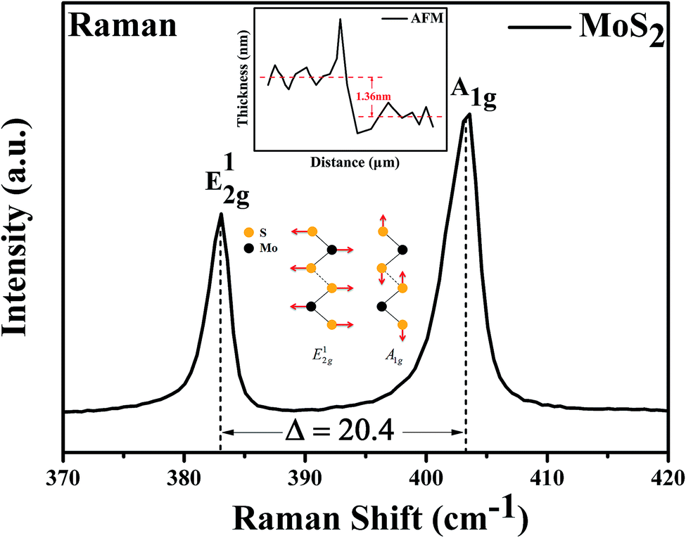 | ||
| Fig. 2 Raman spectrum of the channel material. The number of layers of the MoS2 nanosheet we prepared can be confirmed as bilayer. Inset, the height gradient between the channel material and the underlying substrate was tested by the AFM, the thickness of the MoS2 channel material is 1.36 nm. | ||
The electrical characteristics of the MoS2 FET have a strong impact on the sensitivity of the biosensor. The testing of the electrical properties of the MoS2 nanosheet based FET without glucose solution is shown in Fig. 3. As the output characteristic (Ids–Vds) curve shown in Fig. 3a, the Ids increases with the increase of Vds. Especially in the low voltage region of Vds, it can be observed that the Ids increases linearly with Vds and the curve pass through the original point, indicating that the good ohmic contact was formed between the electrodes and MoS2 layers, which is beneficial to the injection of electrons. The device can be effectively controlled by the Vgs, which is illustrated by the output characteristic curve of the device with different Vgs in Fig. 3a; several important electrical parameters of MoS2 FET can be achieved from the transfer characteristic curve (Ids–Vgs) and the logarithmic image of Ids–Vgs, which was shown in Fig. 3b and its illustrations. According to calculation results: the field-effect mobility (μ) reached 33.5 cm2 V−1 s−1, the transconductance (gm) was 1.7 and the switching current ratio (Ion/Ioff) was as high as 106.
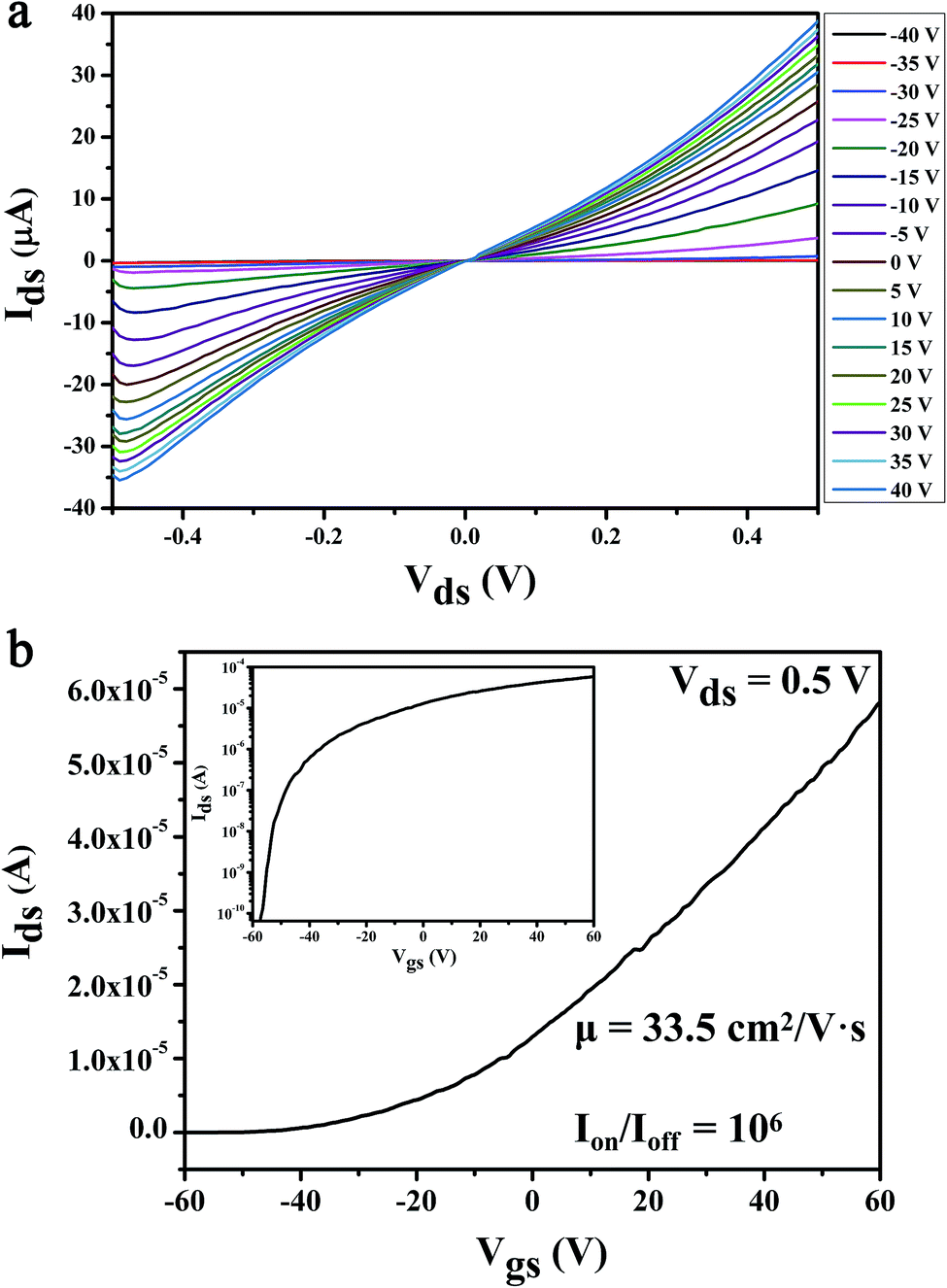 | ||
| Fig. 3 The basic electrical characterization of the MoS2 FET. (a) Output characteristic curve of the device, drain current (Ids) as a function of drain voltage (Vds) with the back gate voltage (Vgs) varying from −40 to 40 V, in a step of 5 V. (b) Transfer characteristic curve of the device, Ids as a function of Vgs with the Vds of 0.5 V. Inset, the logarithmic image of transfer characteristic curve (Ids–Vgs). | ||
Detection of glucose using MoS2 FET based biosensor
In the research of glucose sensing performance, the output characteristic curves were tested with the different glucose concentration. Fig. 4a shown the Ids of MoS2 FET varies with the concentration of glucose solution. This phenomenon can be explained by the enzymatic reaction of glucose with GOx and formation of the products.44 The underlaying sensing mechanism of the glucose biosensor based on bilayer MoS2 FET is attributed to the reaction of H2O2 generated by the oxidation of glucose. The details is that the glucose solution can generate gluconate and hydrogen peroxide (H2O2) after being catalyzed by the glucose oxidase (GOx), and H2O2 will be dissociated and produce hydrogen ions (H+) and electrons (e−). The concentration of electrons increases on the surface of conductive channel of the device with the process of enzymatic reaction. And the conductance of the channel material is increased because the MoS2 is a n-type semiconductor. This is due to the n-doping effect resulting from the direct electron transfer on the surface of the MoS2 nanosheet. There would be a charge transfer from the H2O2 molecules to the MoS2 channel.26,27,44–49 The glucose oxidation reaction is as follows: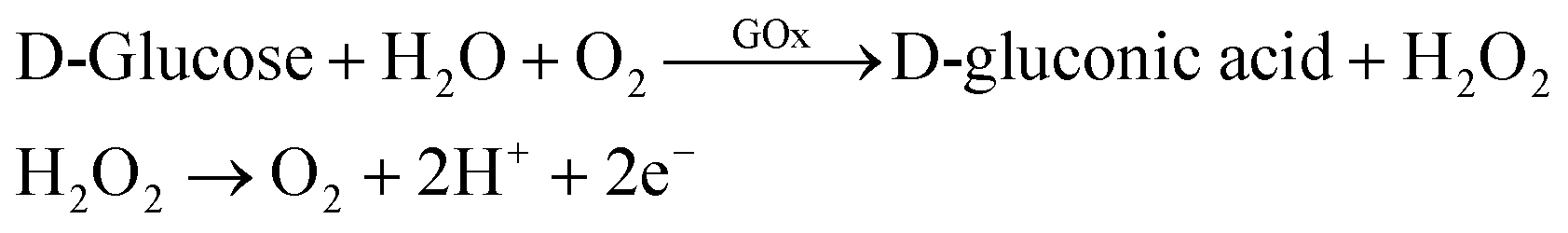
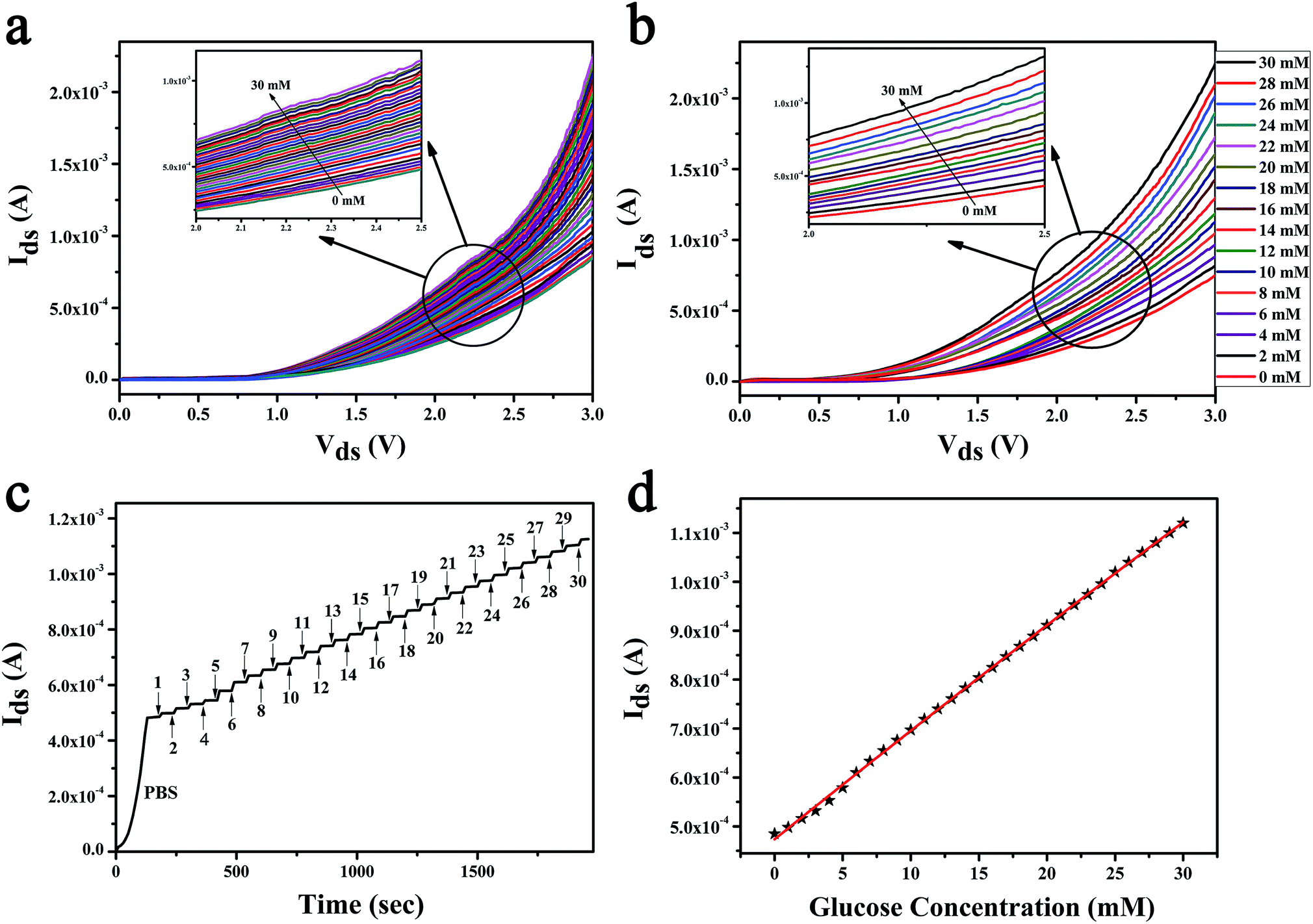 | ||
| Fig. 4 MoS2 FET sensor for glucose sensing. (a) Drain current for an n-type MoS2 FET-based glucose sensor is plotted as a function of Vds for different concentrations of the glucose solution. (b) Repeatability experiments of the glucose sensing. The even number points of glucose concentration values are tested by the device used in the (a). (c) The real time current responses to the fluctuation of glucose concentrations. The glucose responses for the sequential concentration increase at Vgs of 0.5 V and Vds of 2.5 V. (d) The response curve of the MoS2 FET to glucose solution. Ids as a function of glucose concentration which is from 0 to 30 mM. | ||
The repeatability experiments were carried out by the same device and under the same conditions after 45 days. The device was used to test the even number points of glucose concentration values, as shown in Fig. 4b. The results shown that the device has a good stability. The real time sensor response to the addition of different concentration of glucose was shown in the Fig. 4c. The test was started with a pure PBS solution under fixed Vds of 2.5 V and Vgs of 0.5 V. 1 mM glucose solution was first injected at 180 s. And then, the glucose solution with higher concentrations were replaced the last one ever minute thereafter. The relationship between glucose concentration and the electrical parameters of MoS2 FET were shown in Fig. 4d. Then the unknown concentrations of glucose solution can be detected by the Ids of the MoS2 FET (Vgs of 0.5 V, Vds of 2.5 V), as illustrated in Table 1.
| Ids (mA) | 0.498 | 0.516 | 0.532 | 0.553 | 0.579 | 0.610 | 0.633 | 0.655 | 0.676 | 0.697 |
| Glucose (mM) | 1 | 2 | 3 | 4 | 5 | 6 | 7 | 8 | 9 | 10 |
| Ids (mA) | 0.719 | 0.740 | 0.761 | 0.783 | 0.804 | 0.825 | 0.847 | 0.868 | 0.889 | 0.911 |
| Glucose (mM) | 11 | 12 | 13 | 14 | 15 | 16 | 17 | 18 | 19 | 20 |
| Ids (mA) | 0.932 | 0.953 | 0.974 | 0.996 | 1.021 | 1.043 | 1.062 | 1.084 | 1.107 | 1.129 |
| Glucose (mM) | 21 | 22 | 23 | 24 | 25 | 26 | 27 | 28 | 29 | 30 |
Sensitivity test
In order to research the detection limit and the sensitivity of the MoS2 FET based biosensor, the glucose solution with extremely low concentration which from 0 nM to 1 μM was detected by the change of output characteristic curves, as shown in Fig. 5a.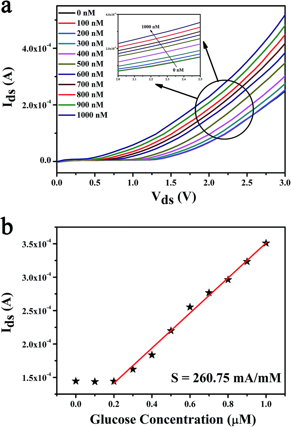 | ||
| Fig. 5 MoS2 FET sensor for ultra low concentration glucose sensing. (a) The detection limit of the biosensor based on MoS2 FET observed by the output characteristic curve is 300 nM. (b) Drain current as a function of glucose concentration which ranges from 0 to 1 μM at Vgs of 0.5 V and Vds of 2.5 V. By calculation, the sensitivity of our biosensor has been achieved as high as 260.75 mA mM−1. | ||
The detection limit of our biosensor is 300 nM. The Ids as a function of glucose concentration was shown in Fig. 5b. The sensitivity of the glucose biosensor can be calculated as high as 260.75 mA mM−1. And the response time (<1 s) and the linear regions (300 nM to 30 mM) were tested in our experiments. Analytical features of some reported for glucose biosensors based on the FET are summarized in the Table 2 and compared with those parameters obtained from our results using bilayer MoS2 FET. As shown in Table 2, the proposed ZnO-based glucose biosensor shown higher sensitivity,28 shorter response time45 and wider linear dynamic range50 than those previous reports.26,27,46,47,51–55 And the detection limit of the reduced graphene oxide/carboxylated polypyrrole nanotube (rGO/C-PPy NT) FET based biosensor42 was better than other glucose biosensors.26–28,45–47,50–55 Compared with previous researches, the bilayer MoS2-based FET we prepared show significant advantages in high sensitivity detection of extremely low concentration glucose solution.
| Modified surface | Sensitivity | LDR | DL | Response time | Reference |
|---|---|---|---|---|---|
| a LDR, linear dynamic range; DL, detection limit; CPNTs, carboxylated polypyrrole nanotubes; rGO/C-PPy NT, reduced graphene oxide/carboxylated polypyrrole nanotube; SGGT, solution gated graphene transistors; ZnO NRs, ZnO nanorods; CNTFs, carbon nanotube thin films; MWCNTCOOH/PAN, multi-walled carbon nanotubes-polyaniline nanocomposite; nr, not reported. | |||||
| CPNTs | nr | 0.5–20 mM | nr | 5–10 s | Yoon et al. (2008) |
| Graphene | nr | 3.3–10.9 mM | 3.3 mM | nr | Kwak et al. (2012) |
| Graphene | 0.4086 mA mM−1 | 1.25–10 mM | 1.25 mM | nr | Cagang et al. (2016) |
| Graphene | 2.5 μA mM−1 | 0.1–10 mM | 0.1 mM | nr | You and Pak (2014) |
| rGO/C-PPy NT | nr | nr | 1 nM | <1 s | Park et al. (2015) |
| SGGT | 17.3 mV M−1 | 0.5–300 μM | 0.5 μM | nr | Zhang et al. (2014) |
| ZnO NRs | 10 mA cm−2 mM−1 | 0.001–45 mM | 1 μM | nr | Ahmada et al. (2013) |
| CNTFs | 0.302 mV mg−1 dl−1 | 60–360 mg dl−1 | 60 mg dL−1 | nr | Tsai et al. (2013) |
| ZnO NRs | 38.9 μA mM−1 | 800 nM to 25 mM | 800 nM | nr | Lee and Chiu (2015) |
| ZnO | nr | 1–100 μM | 1 μM | <0.1 s | Ali et al. (2009) |
| ZnO | 2.7 A mM−1 | 10–30 mM | nr | 20 s | Yano et al. (2012) |
| MWCNTCOOH/PAN | nr | 0.005–50 mM | 0.5 mM | 10 s | Fathollahzadeh et al. (2016b) |
| Bilayer MoS2 | 260.75 mA mM−1 | 300 nM to 30 mM | 300 nM | <1 s | Our research |
Conclusions
In summary, a biosensor based on the bilayer MoS2 back-gate FET was fabricated and demonstrated for glucose detection successfully in our research. In particular, the glucose concentration was detected by the MoS2 FET for the first time. Considering the concentration of the fasting blood ranges from 3.9 to 6.1 mM, the concentration was detected in the range of 0–30 mM by the glucose biosensor we prepared. Through measurements of the Ids, the fabricated MoS2 FET biosensor shown a good sensing performance. The high sensitivity of 260.75 mA mM−1 was achieved for the detection of glucose solution which has the extremely low concentration level (300 nM). The other advantages of our biosensor such as short response time (<1 s), good stability, small size and trace detection were all demonstrated in our studies. This article open up a new path for the applications about the MoS2 FET. In practical sensing applications, we can design a bio-integrated circuit which contains a FET, an operational amplifier, a comparator and an LED to achieve the macroscopic, fast detection. That can be used to realize the miniaturization and real-time detection of human blood glucose concentration in the future.Conflicts of interest
There are no conflicts to declare.Acknowledgements
This work is supported by the “111” Project of China (D17017), the National Natural Science Foundation of China (21703017, 11674038, 61404009), the Advance Research Project of Weapon and Equipment (61404140201), the Project of Education Department of Jilin Province (JJKH20170611KJ), and the Developing Project of Science and Technology of Jilin Province (20160520117JH).References
- D. Lembke, S. Bertolazzi and A. Kis, Acc. Chem. Res., 2015, 48, 100–110 CrossRef CAS PubMed.
- D. Krasnozhon, D. Lembke, C. Nyffeler, Y. Leblebici and A. Kis, Nano Lett., 2014, 14, 5905–5911 CrossRef CAS PubMed.
- K. F. Mak, C. Lee, J. Hone, J. Shan and T. F. Heinz, Phys. Rev. Lett., 2010, 105, 136805 CrossRef PubMed.
- W. X. Gu, J. Y. Shen and X. Y. Ma, Nanoscale Res. Lett., 2014, 9, 100 CrossRef PubMed.
- T. Kawanago and S. Oda, Appl. Phys. Lett., 2016, 108, 041605 CrossRef.
- Y. Chen, X. D. Wang, P. Wang, H. Huang, G. J. Wu, B. Tian, Z. C. Hong, Y. T. Wang, S. Sun, H. Sheng, J. L. Wang, W. D. Hu, J. L. Sun, X. J. Meng and J. H. Chu, ACS Appl. Mater. Interfaces, 2016, 8, 32083–32088 CAS.
- D. J. Late, B. Liu, H. S. S. R. Matte, V. P. Dravid and C. N. R. Rao, ACS Nano, 2012, 6, 5635–5641 CrossRef CAS PubMed.
- D. Jariwala, V. K. Sangwan, D. J. Late, J. E. Johns, V. P. Dravid, T. J. Marks, L. J. Lauhon and M. C. Hersam, Appl. Phys. Lett., 2013, 102, 173107 CrossRef.
- P. K. Kannan, D. J. Late, H. Morgan and C. S. Rout, Nanoscale, 2015, 7, 13293–13312 RSC.
- D. J. Late, P. A. Shaikh, R. Khare, R. V. Kashid, M. Chaudhary, M. A. More and S. B. Ogale, ACS Appl. Mater. Interfaces, 2014, 6, 15881–15888 CAS.
- D. Sarkar, W. Liu, X. J. Xie, A. C. Anselmo, S. Mitragotri and K. Banerjee, ACS Nano, 2014, 4, 3992–4003 CrossRef PubMed.
- W. Yang, K. R. Ratinac, S. P. Ringer, P. Thordarson, J. J. Gooding and F. Braet, Angew. Chem., Int. Ed., 2010, 49, 2114–2138 CrossRef CAS PubMed.
- M. S. Makowski and A. Ivanisevic, Small, 2011, 7(14), 1863–1875 CrossRef CAS PubMed.
- Y. Ohno, K. Maehashi, Y. Yamashiro and K. Matsumoto, Nano Lett., 2009,(9), 3318–3322 CrossRef CAS PubMed.
- Y. Ohno, K. Maehashi and K. Matsumoto, J. Am. Chem. Soc., 2010, 132, 18012–18013 CrossRef CAS PubMed.
- M. Dankerl, M. V. Hauf, A. Lippert, L. H. Hess, S. Birner, I. D. Sharp, A. Mahmood, P. Mallet, J. Y. Veuillen, M. Stutzmann and J. A. Garrido, Adv. Funct. Mater., 2010, 20, 3117–3124 CrossRef CAS.
- D. J. Late, Y. K. Huang, B. Liu, J. Acharya, S. N. Shirodkar, J. J. Luo, A. Yan, D. Charles, U. V. Waghmare, V. P. Dravid and C. N. R. Rao, ACS Nano, 2013, 7, 4879–4891 CrossRef CAS PubMed.
- G. Yoo, H. Park, M. Kim, W. G. Song, S. Jeong, M. H. Kim, H. Lee, S. W. Lee, Y. K. Hong, M. G. Lee, S. Lee and S. Kim, Nano Res., 2017, 10(3), 767–775 CrossRef CAS.
- B. Liu, L. Chen, G. Liu, A. N. Abbas, M. Fathi and C. Zhou, ACS Nano, 2014, 8, 5304–5314 CrossRef CAS PubMed.
- J. W. Huang, Y. Q. He, J. Jin, Y. R. Li, Z. P. Dong and R. Li, Electrochim. Acta, 2014, 136, 41–46 CrossRef CAS.
- J. W. Huang, Z. P. Dong, Y. D. Li, J. Li, J. Wang, H. D. Yang, S. W. Li, S. J. Guo, J. Jin and R. Li, Sens. Actuators, B, 2013, 182, 618–624 CrossRef CAS.
- X. Y. Li and X. Z. Du, Sens. Actuators, B, 2017, 239, 536–543 CrossRef CAS.
- L. M. Lu, H. B. Li, F. L. Qu, X. B. Zhang, G. L. Shen and R. Q. Yu, Biosens. Bioelectron., 2011, 26, 3500–3504 CrossRef CAS PubMed.
- K. I. Ozoemena and T. Nyokong, Electrochim. Acta, 2006, 51, 5131–5136 CrossRef CAS.
- Y. Y. Su, B. B. Luo and J. Z. Zhang, Anal. Chem., 2016, 88, 1617–1624 CrossRef CAS PubMed.
- Y. H. Kwak, D. S. Choi, Y. N. Kim, H. Kim, D. H. Yoon, S. S. Ahn, J. W. Yang, W. S. Yang and S. Seo, Biosens. Bioelectron., 2012, 37, 82–87 CrossRef CAS PubMed.
- H. Yoon, S. Ko and J. Jang, J. Phys. Chem. B, 2008, 112, 9992–9997 CrossRef CAS PubMed.
- M. Yano, K. Koike, K. Ogata, T. Nogami, S. Tanabe and S. Sasa, Phys. Status Solidi, 2012, 9, 1570–1573 CrossRef CAS.
- Y. M. Lin, K. A. Jenkins, A. Valdes-Garcia, J. P. Small, D. B. Farmer and P. Avouris, Nano Lett., 2008, 9, 422–426 CrossRef PubMed.
- P. Wei, N. Liu, H. R. Lee, E. Adijanto, L. Ci, B. D. Nabb, J. Q. Zhong, J. Park, W. Chen, Y. Cui and Z. Bao, Nano Lett., 2013, 13, 1890–1897 CrossRef CAS PubMed.
- Y. M. Lin, C. Dimitrakopoulos, K. A. Jenkins, D. B. Farmer, H. Y. Chiu, A. Grill and P. Avouris, Science, 2010, 327, 662 CrossRef CAS PubMed.
- S. Lebegue and O. Eriksson, Phys. Rev. B: Condens. Matter Mater. Phys., 2009, 79, 115409 CrossRef.
- A. Splendiani, L. Sun, Y. Zhang and F. Wang, Nano Lett., 2010, 10, 1271 CrossRef CAS PubMed.
- A. Kuc, N. Zibouche and T. Heine, Phys. Rev. B: Condens. Matter Mater. Phys., 2011, 83, 245213 CrossRef.
- S. L. Li, K. Komatsu, S. Nakaharai, Y. F. Lin, M. Yamamoto, X. F. Duan and K. Tsukagonshi, ACS Nano, 2014, 12836–12842 CrossRef CAS PubMed.
- S. Kim, A. Konar, W. S. Hwang, J. H. Lee, J. Lee, J. Yang, C. Jung, H. Kim, J. Yoo, J. Y. Choi, Y. W. Jin, S. Y. Lee, D. Jena, W. Choi and K. Kim, Nat. Commun., 2012, 20, 1038 Search PubMed.
- B. W. H. Baugher, H. O. H. Churchill, Y. Yang and P. J. Herrero, Nano Lett., 2013, 13, 4212–4216 CrossRef CAS PubMed.
- H. Li, Z. Y. Yin, Q. Y. He, H. Li, X. Huang, G. Lu, D. W. H. Fam, A. L. Y. Tok, Q. Zhang and H. Zhang, Small, 2012, 8, 63–67 CrossRef CAS PubMed.
- A. S. Pawbake, M. S. Pawar, S. R. Jadkar and D. J. Late, Nanoscale, 2016, 8, 3008–3018 RSC.
- M. X. Ye, D. Winslow, D. Y. Zhang, R. Pandey and Y. K. Yap, Photonics, 2015, 2, 288–307 CrossRef CAS.
- S. Tongay, W. Fan, J. Kang, J. Park, U. Koldemir, J. Suh, D. S. Narang, K. Liu, J. Ji, J. Li, R. Sinclair and J. Wu, Nano Lett., 2014, 14, 3185 CrossRef CAS PubMed.
- X. Li, J. H. Li, X. H. Wang, J. X. Hu, X. Fang, X. Y. Chu, Z. P. Wei and J. J. Shan, Integr. Ferroelectr., 2014, 158, 26–42 CrossRef CAS.
- C. G. Lee, H. G. Yan, L. E. Brus, T. F. Heinz, J. Hone and S. Ryu, ACS Nano, 2010, 5, 2695–2700 CrossRef PubMed.
- M. Fathollahzadeh, M. Hosseini, B. Haghighi and M. Fathipour, Anal. Chim. Acta, 2016, 924, 99–105 CrossRef CAS PubMed.
- R. Ahmad, N. Tripathy and Y. B. Hahn, Biosens. Bioelectron., 2013, 45, 281–286 CrossRef CAS PubMed.
- M. Zhang, C. Z. Liao, C. H. Mak, P. You, C. L. Mak and F. Yan, Sci. Rep., 2015, 5, 8311 CrossRef CAS PubMed.
- W. L. Tsai, Y. S. Chien, P. Y. Yang, I. C. Lee, K. Y. Wang and H. C. Cheng, Sens. Actuators, A, 2013, 204, 31–36 CrossRef CAS.
- Y. H. Lin, C. P. Chu, C. F. Lin, H. H. Liao, H. H. Tsai and Y. Z. Juang, Biomed. Microdevices, 2015, 17, 111 CrossRef PubMed.
- X. You and J. J. Pak, Sens. Actuators, B, 2014, 202, 1357–1365 CrossRef CAS.
- S. M. U. Ali, O. Nur, M. Willander and B. Danielsson, IIEEE Trans. Nanotechnol., 2009, 6, 678–683 Search PubMed.
- A. A. Cagang, I. H. Abidi, A. Tyagi, J. Hu, F. Xu, T. J. Lu and Z. Luo, Anal. Chim. Acta, 2016, 917, 101–106 CrossRef CAS PubMed.
- X. Q. You and J. J. Pak, Sens. Actuators, B, 2014, 202, 1357–1365 CrossRef CAS.
- J. W. Park, C. Lee and J. Jang, Sens. Actuators, B, 2015, 208, 532–537 CrossRef CAS.
- C. T. Lee and Y. S. Chiu, Sens. Actuators, B, 2015, 210, 756–761 CrossRef CAS.
- M. Fathollahzadeh, M. Hosseini, B. Haghighi, M. Kolahdouz and M. Fathipour, Anal. Chim. Acta, 2016, 924, 99–105 CrossRef CAS PubMed.
| This journal is © The Royal Society of Chemistry 2018 |