
 Open Access Article
 This Open Access Article is licensed under a
 Creative Commons Attribution 3.0 Unported Licence
Switching properties of epitaxial La0.5Sr0.5CoO3/Na0.5Bi0.5TiO3/La0.5Sr0.5CoO3 ferroelectric capacitor
J. M. Song ab,
L. H. Luoc,
X. H. Daia,
A. Y. Songa,
Y. Zhoua,
Z. N. Lia,
J. T. Lianga and
B. T. Liu*a
ab,
L. H. Luoc,
X. H. Daia,
A. Y. Songa,
Y. Zhoua,
Z. N. Lia,
J. T. Lianga and
B. T. Liu*a
aHebei Key Lab of Optic-Electronic Information and Materials, College of Physics Science & Technology, Hebei University, Baoding 071002, China. E-mail: btliu@hbu.cn
bCollege of Science, Agriculture University of Hebei, Baoding 071001, China
cCollege of Science, Ningbo University, Ningbo 315211, China
First published on 24th January 2018
Abstract
La0.5Sr0.5CoO3/Na0.5Bi0.5TiO3/La0.5Sr0.5CoO3 (LSCO/NBT/LSCO) ferroelectric capacitors have been successfully fabricated on (001) SrTiO3 substrate, in which the LSCO film is prepared by magnetron sputtering and the NBT film by pulsed laser deposition. Both X-ray diffraction and transmission electron microscopy techniques confirm that the (001) oriented LSCO/NBT/LSCO heterostructure is epitaxially grown on SrTiO3 substrate. The remnant polarization, coercive field and relative dielectric constant of the LSCO/NBT/LSCO capacitor, measured at 250 kV cm−1, are 15.6 μC cm−2, 47 kV cm−1 and 559, respectively. Moreover, the capacitor possesses very good fatigue-resistance, and less pulse width dependence as well as piezoelectric properties (d33 = 145 pm V−1). It is found that the leakage current density of the LSCO/NBT/LSCO capacitor meets well with ohmic conduction behavior at applied fields lower than 55 kV cm−1 and bulk-limited space charge-limited conduction at the fields higher than 55 kV cm−1.
1. Introduction
Ferroelectric thin film materials have been extensively investigated due to their good ferroelectric, dielectric, piezoelectric and optical properties for various kinds of applications, e.g. phase shifters, microelectromechanical systems, sensors, and ferroelectric random access memory (FeRAM).1–3 Lead based Pb(Zr1−xTix)O3 (PZT) films are intensively studied worldwide including by our group due to their large remnant polarization and small coercive voltage.4–6 However, PZT films are not environmentally friendly materials, thus many efforts have been made to develop lead-free new type ferroelectric materials.7,8 Sodium bismuth titanate, Na0.5Bi0.5TiO3 (NBT), with A-site composite perovskite structure is considered as an excellent candidate to replace lead based ferroelectric materials.9,10 Recently, we have successfully prepared a single-phase high quality NBT bulk material by solid state reaction method, and investigated the optical properties and ferroelectric properties.11,12 The Na0.5Bi0.5TiO3 ceramics have good ferroelectric properties at room temperature and relatively high Curie temperature (320 °C), which makes ferroelectric NBT film based device very promising.13 Polycrystalline NBT films with good ferroelectric remnant polarization (∼11.9 μC cm−2) have been grown on Pt/Ti/SiO2/Si substrates using various methods such as radio-frequency magnetron sputtering and metal organic decomposition process.14,15 Compared to the polycrystalline films, it is believed that the highly oriented ferroelectric films (especially the epitaxial films) can possess higher polarization and less leakage current due to the lack of grain boundaries in the epitaxial films. Highly (111) oriented NBT film was prepared on Pt/Ti/SiO2/Si substrate by a sol–gel process, it is found that the remnant polarization and coercive field are 20.6 μC cm−2 and 112 kV cm−1, respectively.16 (001) and (011) oriented epitaxial NBT films have been successfully fabricated on platinum coated MgO and SrTiO3 substrates by pulsed laser deposition, and very good dielectric and ferroelectric properties have been reported.17,18 Compared to Pt electrode, the cheaper LSCO electrode can provide oxide/oxide (LSCO/NBT) interface, different from the metal/oxide (Pt/NBT) interface, which may further impact the NBT physical properties. From the viewpoint of our best knowledge, no results have been reported on the fabrication and characterization of epitaxial NBT capacitor sandwiched by oxide electrodes. In this paper, we report on the fabrication of the epitaxial LSCO/NBT/LSCO/SrTiO3 (STO) heterostructure, and the structural and switching properties of the LSCO/NBT/LSCO ferroelectric capacitors have been systematically investigated.2. Experimental
Briefly, the Pt/LSCO/NBT/LSCO/STO heterostructure was prepared by a multi-step procedure. Step 1: 60 nm-thick LSCO thin film was deposited on (001) STO single crystal substrate by magnetron sputtering at room temperature under the following conditions: Ar![[thin space (1/6-em)]](https://www.rsc.org/images/entities/char_2009.gif) :O2 = 3:1, power = 30 W. Post-annealing was conducted at 550 °C in a 1 atm oxygen-flowing tube furnace. Step 2: Na0.5Bi0.5TiO3 target with 10% excessive bismuth and 10% sodium was used during deposition to compensate the loss of bismuth and sodium due to the strong volatility of bismuth and sodium. 250 nm-thick NBT film was further deposited on the LSCO/STO heterostructure by pulsed laser deposition at 550 °C and 7.5 Pa oxygen deposition pressure. The target and substrate distance was 4.5 cm; the laser energy density and repetition rate were 2 J cm−2 and 5 Hz, respectively. Step 3: 60 nm-thick LSCO film and 70 nm thick Pt were sequentially deposited by magnetron sputtering on the surface of the NBT/LSCO/STO heterostructure through a shadow mask to get 7.85 × 10⁻⁵ cm2 circular pads as the top electrodes of the capacitors. The Pt film is used to improve the electrical contact between the measurement tip and LSCO. The Pt/LSCO/NBT/LSCO/STO heterostructure was further annealed at 550 °C in an oxygen-flowing tube furnace in order to make the as-grown top LSCO film crystallized. The crystallinity and phase of the sample was characterized by X-ray diffraction (XRD) and the cross-sectional interfaces of NBT/LSCO/STO heterostructure were investigated using transmission electron microscopy (TEM). The ferroelectric properties and leakage current behavior of the LSCO/NBT/LSCO capacitor were studied using a precision LC unit from Radiant Technologies. The dielectric and piezoelectric properties were measured using an Agilent 4294A and piezoresponse force microscope (PFM-Asylum Research), respectively.
:O2 = 3:1, power = 30 W. Post-annealing was conducted at 550 °C in a 1 atm oxygen-flowing tube furnace. Step 2: Na0.5Bi0.5TiO3 target with 10% excessive bismuth and 10% sodium was used during deposition to compensate the loss of bismuth and sodium due to the strong volatility of bismuth and sodium. 250 nm-thick NBT film was further deposited on the LSCO/STO heterostructure by pulsed laser deposition at 550 °C and 7.5 Pa oxygen deposition pressure. The target and substrate distance was 4.5 cm; the laser energy density and repetition rate were 2 J cm−2 and 5 Hz, respectively. Step 3: 60 nm-thick LSCO film and 70 nm thick Pt were sequentially deposited by magnetron sputtering on the surface of the NBT/LSCO/STO heterostructure through a shadow mask to get 7.85 × 10⁻⁵ cm2 circular pads as the top electrodes of the capacitors. The Pt film is used to improve the electrical contact between the measurement tip and LSCO. The Pt/LSCO/NBT/LSCO/STO heterostructure was further annealed at 550 °C in an oxygen-flowing tube furnace in order to make the as-grown top LSCO film crystallized. The crystallinity and phase of the sample was characterized by X-ray diffraction (XRD) and the cross-sectional interfaces of NBT/LSCO/STO heterostructure were investigated using transmission electron microscopy (TEM). The ferroelectric properties and leakage current behavior of the LSCO/NBT/LSCO capacitor were studied using a precision LC unit from Radiant Technologies. The dielectric and piezoelectric properties were measured using an Agilent 4294A and piezoresponse force microscope (PFM-Asylum Research), respectively.
3. Results and discussion
Fig. 1(a) presents the theta–2theta XRD spectrum of the NBT/LSCO/STO heterostructure. Besides the STO peaks, only (001), (002) diffraction peaks of NBT and LSCO are observed without any detectable secondary phase or diffraction peaks from other directions, indicating that both NBT and LSCO films are highly (001) oriented. In order to further prove the epitaxial property of NBT film on the LSCO/STO heterostructure, we performed the phi-scan of (110) plane of NBT film. As shown in the inset of Fig. 1, the four evenly spaced peaks with spacing of 90° reveal that the NBT film was epitaxially grown on NBT/LSCO/STO heterostructure. Fig. 1(b) presents the TEM image of the NBT/LSCO and LSCO/STO interfaces, no obvious interdiffusion can be found at the interfaces. Selected area diffraction (SAED) of NBT and LSCO films derived from fast Fourier transform (FFT) are respectively presented in the Fig. 1(b), indicating both NBT and LSCO are single crystalline films. Fig. 1(c) shows a typical high-resolution TEM image of the LSCO/STO heterostructure and single crystalline LSCO film is epitaxially grown on the surface of (001) STO substrate. The orientation relationship of these two layers is (001)LSCO//(001)STO and [100]LSCO//[100]STO. Fig. 1(d) shows a HRTEM image of the NBT/LSCO interface region viewed along the [100] zone axis of STO substrate. The interface is atomically sharp, indicating a very good epitaxial growth relationship exists between NBT and LSCO. The orientation relationship between the NBT film and the LSCO film in the NBT/LSCO heterostructure is as follows: (001)NBT//(001)LSCO, [100]NBT//[100]LSCO, which is expected since the NBT (0.389 nm) has a good lattice match with the underlying LSCO (0.384 nm). Based on the SAED of NBT film in the Fig. 1(b), the lattice constants are 0.390 nm and 0.398 nm for the in-plane (a axis) and the out-plane (c axis), respectively. The c axis constant is consistent with the value, 0.397 nm, obtained from the XRD measurement. We should note that the out-plane lattice constant of NBT (0.397 nm) is larger than that of its bulk material (0.389 nm). A compressive force exists in the NBT film when NBT is epitaxially grown on LSCO surface so that out-plane lattice constant of NBT becomes larger. The polarization Ps of a ferroelectric material is related to its tetragonality, (Ps)2 ∝ (c/a − 1)2, and the tetragonality (c/a = 1.02) of the epitaxial NBT film in the LSCO/NBT/LSCO heterostructure is larger than its bulk value (c/a = 1.002), which is favorable for the NBT film to have a larger remnant polarization.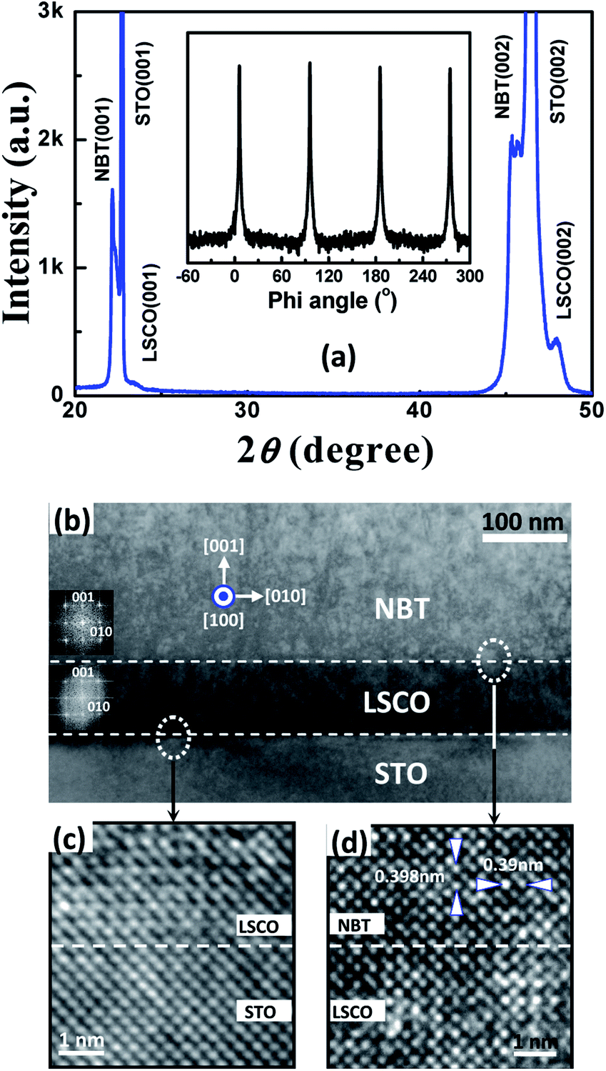 | ||
| Fig. 1 XRD spectrum of NBT/LSCO/STO heterostructure, the inset is the phi-scan pattern of the NBT film (a). TEM image of the cross sectional image of the NBT/LSCO/STO heterostructure (b). The high-resolution TEM images of LSCO/STO (c) and NBT/LSCO (d). | ||
A typical ferroelectric hysteresis loop of the LSCO/NBT/LSCO capacitor, measured at 250 kV cm−1 bias electric field and 1 kHz frequency using capacitive method, is illustrated in Fig. 2(a). A saturated ferroelectric loop can be obtained with a remnant polarization, 15.6 μC cm−2, and a small coercive field, 47 kV cm−1. The inset at the top left-hand side of Fig. 2(a) is the phase PFM images, which recorded for sample NBT after square areas of (7 × 7 μm2) and (4 × 4 μm2) have been polarized (black region) and reverse polarized (white region) by applying bias electric field −250 kV cm−1 and 250 kV cm−1, respectively. We can see the polarization switching within these domains as square areas defined by black and white contrasts, characteristic of each orientation of the polarization can be observed. This means that (001) epitaxial NBT thin film has good reversal memory properties. The switchable polarization, ΔP, is defined as the difference between the switched (P*) and nonswitched (P^) polarization. The inset at the bottom right-hand side of Fig. 2(a) demonstrates the relation of switchable polarization with applied electric field. We can see that the switchable polarization increases rapidly with the increase of the applied electric field, and it is saturated when the applied electric field is greater than 100 kV cm−1. Fig. 2(b) shows the pulse width dependence of the LSCO/NBT/LSCO capacitor measured at bias electric field 250 kV cm−1 with a pulse delay time of 1 s. It can be seen that the switchable polarization slightly increases with the increase of the pulse width, which is favorable to the high speed ferroelectric memories. In addition, fatigue is also an important parameter to characterize ferroelectric film for ferroelectric memories. In this experiment, the fatigue characteristic of the LSCO/NBT/LSCO capacitor was tested at bias electric field 250 kV cm−1 and 1 MHz frequency with a pulse delay time of 1 s. As shown in Fig. 2(c), no obvious degradation can be found from the polarizations of the capacitor up to 1010 switching cycles. The inset of Fig. 2(c) presents the hysteresis loops before and after the fatigue test, in which no obvious difference can be found from the hysteresis loops, further indicating that the epitaxial LSCO/NBT/LSCO capacitor has very good fatigue resistance characteristic. Fig. 2(d) demonstrates the relation of dielectric constant and loss tangent with applied electric field for the LSCO/NBT/LSCO capacitor at a frequency of 10 kHz. The tunability of 50.1% at the maximum applied field of 250 kV cm−1 is obtained, in which the tunability is defined19
 | (1) |
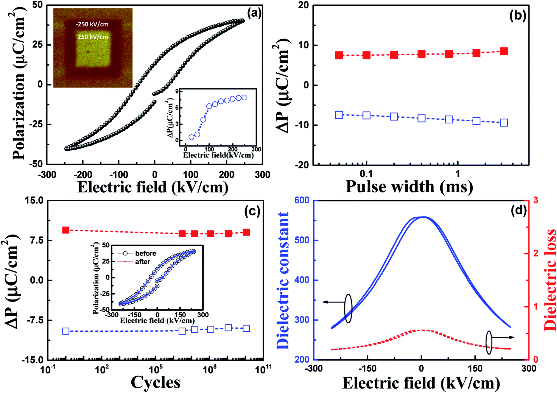 | ||
| Fig. 2 Ferroelectric hysteresis loop of the LSCO/NBT/LSCO capacitor, the inset at the top left-hand side shows the phase PFM images of NBT film, the inset at the bottom right-hand side presents relation of ΔP vs. applied field (a). Relation of ΔP vs. pulse width of the LSCO/NBT/LSCO capacitor (b). Relation of ΔP vs. frequency of the LSCO/NBT/LSCO capacitor, the inset is the ferroelectric hysteresis loops before and after fatigue tests (c). Relation of dielectric constant and dielectric loss vs. applied field of the LSCO/NBT/LSCO capacitor (d). | ||
In formula (1), εmin is the minimum value of the dielectric constant at the maximum applied field, εmax is the maximum value of the dielectric constant at the applied field of 0 kV cm−1. The dielectric constant and dielectric loss of the (001) epitaxial NBT film measured at 10 kHz are 559 and 0.19, respectively.
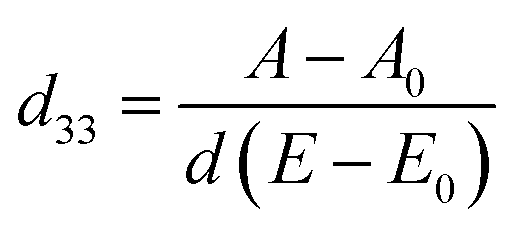
To understand the local switching behavior of the NBT thin films in ferroelectrics, the piezoresponse force microscope PFM (Asylum Research, Cypher, American) was used to characterize piezoelectric properties of the NBT film. Since the effective piezoelectric coefficient d33 can reflect the most essential piezoelectric effect of piezoelectric film material.20 Measurement of d33 was achieved by keeping the PFM tip fixed above the local point of NBT film and applying an electric field from −500 to 500 kV cm−1, while recording the piezoresponse signal amplitude (A) and applied field (E). In the measurements, a bias voltage of 800 mV and a resonance frequency of 320 Hz were applied on the conductive test probe. According to the law of the converse piezoelectric effect, the relationship between amplitude (A) and applied field (E) can be described as follows:21
 | (2) |
In formula (2), d is the initial thickness of the films before deformation, A0 and E0 are the piezoelectric deformation and electric field of the intersection, respectively. The piezoelectric hysteresis loop (d33–E) of NBT film is calculated from the A–E curve based on eqn (1). Fig. 3(a) and (b) displays the corresponding piezoelectric phase–electric field loop and typical piezoelectric response butterfly loop. In the piezoelectric phase electric field loop, the film exhibits a significant 180° domain flip. As can be seen, a typical well-shaped A–E “butterfly” loop is obtained with a amplitude maximum of 1.82 nm appearing at 475 kV cm−1. This result shows a strain as high as ∼0.7% (A/d) and indicates that the (00l) orientation of the epitaxial NBT film has a very good piezoelectricity. In addition, at −205 kV cm−1, the d33 piezoelectric coefficients reached the 145 pm V−1, which is relative higher than the reported NBT-based films.22–24
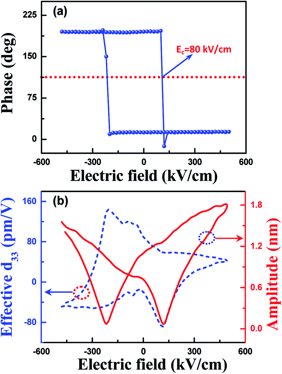 | ||
| Fig. 3 Piezoelectricity of the NBT film obtained by PFM. (a) Phase loop of the NBT film. (b) Ferroelectric butterfly loop and the corresponding piezoelectric hysteresis loop of the NBT film. | ||
Leakage current is an important parameter of the electrical properties of ferroelectric capacitor related to thermal effect and energy loss so that minimum leakage current density is ideal for the real capacitors used in the ferroelectric memories. Four kinds of leakage mechanisms have been proposed for ferroelectric perovskite oxides: the ohmic conduction, the bulk-limited space-charge-limited conduction (SCLC), the bulk-limited Poole–Frenkel emission and the interface-limited Schottky emission.25–28 Fig. 4 shows the relationship between the leakage current density J and the electric field E for the LSCO/NBT/LSCO ferroelectric capacitor. The leakage current density at the applied electric field of 250 kV cm−1 is 3.0 × 10⁻³ A cm−2. The leakage current curve was re-plotted as shown in the inset at the left-hand side and the right-hand side of Fig. 4 in order to further characterize the conduction mechanisms of the LSCO/NBT/LSCO capacitor in different electric field ranges. We can see two kinds of leakage behaviors account for the leakage current characteristic of the LSCO/NBT/LSCO capacitor, and 55 kV cm−1 is the transitional point for the two different leakage current mechanisms. The inset at the left-hand side of Fig. 4 demonstrates the linear relation of log(J) versus log(E) of the LSCO/NBT/LSCO capacitor for the low electric field region, whose slope of 1.15 is close to 1.0, implying ohmic-like conduction for the low electric field region. The relation between current density and electric field for the SCLC is given by
 | (3) |
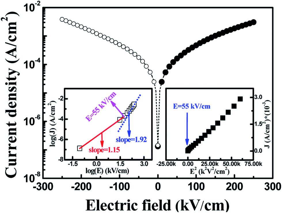 | ||
| Fig. 4 Leakage current density vs. applied electric fields of the LSCO/NBT/LSCO capacitor. The inset at the left-hand side presents relation of log(J) vs. log(E). The inset at the right-hand side presents relation of J vs. E2. | ||
In formula (3), J is the current density, E is electric field, μ is the magnetic permeability, ε is the permittivity, d is film thickness. Regarding high field region, a straight line can be yielded using the relation of J versus E2, as shown in the inset at the right-hand side of Fig. 4, indicating SCLC conduction accounts for the conduction of the capacitor when the applied electric field is higher than 55 kV cm−1. Big differences can be found from the leakage current behavior between LSCO/NBT/LSCO capacitor and Pt/NBT/Pt capacitors.17 The current density of the LSCO/NBT/LSCO capacitor is 3.0 × 10⁻³ A cm−2, while it is 1.4 × 10⁻² A cm−2 for the Pt/NBT/Pt capacitor measured at the same electric field of 250 kV cm−1. The J–E curves of LSCO/NBT/LSCO capacitor for both positive and negative applied fields are very symmetric, however, very different leakage conduction behaviors can be found for the Pt/NBT/Pt capacitor. Moreover, the leakage current behavior of the Pt/NBT/Pt capacitor is mainly attributed to the interface-limited Schottky emission for the high electric field range, which is different from the leakage conduction behavior (SCLC) for the LSCO/NBT/LSCO capacitor. This difference can be ascribed to the fact that Pt and LSCO have different intrinsic property so that different interfaces are formed at Pt/NBT and LSCO/NBT interfaces, which further impact current conduction mechanism of the resulting capacitors.29
4. Conclusions
Compared to the polycrystalline films, the epitaxial LSCO/NBT/LSCO capacitor possesses larger remnant polarization, high dielectric constant and effective piezoelectric coefficient as well as good fatigue resistance and small pulse width dependence. Moreover, the capacitor satisfies ohmic conduction behavior at electric fields lower than 55 kV cm−1 and SCLC behavior above 55 kV cm−1. Our results pave a way for the research and development of lead-free sodium bismuth titanate ferroelectric memories.Conflicts of interest
There are no conflicts to declare.Acknowledgements
This work is supported by the National Natural Science Foundation of China (11374086, 11474174), the Natural Science Foundation of Hebei Province (E2014201188 and E2014201063), and the Foundation of Agriculture University of Hebei (20160614).References
- J. F. Scott, Science, 2007, 315, 954–959 CrossRef CAS PubMed.
- H. Pan, Y. Zeng, Y. Shen, Y. H. Lin, J. Ma, L. Li and C. W. Nan, J. Mater. Chem. A, 2017, 5, 5920–5926 CAS.
- M. Zhu, Z. Du, Q. Liu, B. Chen, S. H. Tsang and E. H. T. Teo, Appl. Phys. Lett., 2016, 108, 233502 CrossRef.
- B. T. Liu, K. Maki, Y. So, V. Nagarajan, R. Ramesh, J. Lettieri, J. H. Haeni, D. G. Schlom, W. Tian, X. Q. Pan, F. J. Walker and R. A. McKee, Appl. Phys. Lett., 2002, 80, 4801 CrossRef CAS.
- Y. J. Fu, G. S. Fu, M. Li, D. M. Jia, Y. L. Jia and B. T. Liu, Appl. Phys. Lett., 2014, 104, 223505 CrossRef.
- T. Zhang, W. Li, W. Cao, Y. Hou, Y. Yu and W. Fei, Appl. Phys. Lett., 2016, 108, 162902 CrossRef.
- I. Katsouras, K. Asadi, W. A. Groen, P. W. M. Blom and D. M. de Leeuw, Appl. Phys. Lett., 2016, 108, 232907 CrossRef.
- D. Gobeljic, V. V. Shvartsman, A. Belianinov, B. Okatan, S. Jesse, S. V. Kalinin, C. Groh, J. Rödel and D. C. Lupascu, Nanoscale, 2016, 8, 2168–2176 RSC.
- G. A. Smolenskii, V. A. Isupov, A. I. Agranovskaya and N. N. Krainik, Sov. Phys. Solid State, 1961, 2, 2651–2654 Search PubMed.
- W. Cao, W. Li, Y. Feng, T. Bai, Y. Qiao, Y. Hou, T. Zhang, Y. Yu and W. Fei, Appl. Phys. Lett., 2016, 108, 202902 CrossRef.
- L. Luo, P. Du, W. Li, W. Tao and H. Chen, J. Appl. Phys., 2013, 114, 124104 CrossRef.
- P. Du, L. Luo, W. Li and Q. Yue, J. Appl. Phys., 2014, 116, 014102 CrossRef.
- A. M. Balakt, C. P. Shaw and Q. Zhang, J. Eur. Ceram. Soc., 2017, 37, 1459–1466 CrossRef CAS.
- Z. H. Zhou, J. M. Xue, W. Z. Li, J. Wang, H. Zhu and J. M. Miao, Appl. Phys. Lett., 2004, 85, 804 CrossRef CAS.
- J. Xu, Y. Liu, R. L. Withers, F. Brink, H. Yang and M. Wang, J. Appl. Phys., 2008, 104, 116101 CrossRef.
- X. G. Tang, J. Wang, X. X. Wang and L. W. Chan, Chem. Mater., 2004, 16, 5293–5296 CrossRef CAS.
- M. Bousquet, J. R. Duclère, C. Champeaux, A. Boulle, P. Marchet, A. Catherinot, A. Wu, P. M. Vilarinho, S. Députier, M. Guilloux-Viry, A. Crunteanu, B. Gautier, D. Albertini and C. Bachelet, J. Appl. Phys., 2010, 107, 034102 CrossRef.
- M. Bousquet, J. R. Duclère, B. Gautier, A. Boulle, A. Wu, S. Députier, D. Fasquelle, F. Rémondière, D. Albertini, C. Champeaux, P. Marchet, M. Guilloux-Viry and P. Vilarinho, J. Appl. Phys., 2012, 111, 104106 CrossRef.
- Y. Wang, B. Liu, F. Wei, Z. Yang and J. Du, Appl. Phys. Lett., 2007, 90, 042905 CrossRef.
- M. Stewart, S. Lepadatu, L. N. McCartney, M. G. Cain, L. Wright, J. Crain, D. M. Newns and G. J. Martyna, APL Mater., 2015, 3, 026103 CrossRef.
- Y. C. Yang, C. Song, X. H. Wang, F. Zeng and F. Pan, Appl. Phys. Lett., 2008, 92, 012907 CrossRef.
- D. Y. Wang, N. Y. Chan, S. Li, S. H. Choy, H. Y. Tian and H. L. W. Chan, Appl. Phys. Lett., 2010, 97, 212901 CrossRef.
- S. K. Acharya, S. K. Lee, J. H. Hyung, Y. H. Yang, B. H. Kim and B. G. Ahn, J. Alloys Compd., 2012, 540, 204–209 CrossRef CAS.
- H. Foronda, M. Deluca, E. Aksel, J. S. Forrester and J. L. Jones, Mater. Lett., 2014, 115, 132–135 CrossRef CAS.
- M. A. Khan, T. P. Comyn and A. J. Bell, Appl. Phys. Lett., 2008, 92, 072908 CrossRef.
- S. Y. Wang, X. Qiu, J. Gao, Y. Feng, W. N. Su, J. X. Zheng, D. S. Yu and D. J. Li, Appl. Phys. Lett., 2011, 98, 152902 CrossRef.
- W. Sun, Z. Zhou, J. Luo, K. Wang and J. F. Li, J. Appl. Phys., 2017, 121, 064101 CrossRef.
- Y. Li, G. I. Ng, S. Arulkumaran, G. Ye, Z. H. Liu, K. Ranjan and K. S. Ang, J. Appl. Phys., 2017, 121, 044504 CrossRef.
- B. Nagaraj, S. Aggarwal and R. Ramesh, J. Appl. Phys., 2001, 90, 375 CrossRef CAS.
| This journal is © The Royal Society of Chemistry 2018 |