
 Open Access Article
 This Open Access Article is licensed under a Creative Commons Attribution-Non Commercial 3.0 Unported Licence
The influence of different Si![[thin space (1/6-em)]](https://www.rsc.org/images/entities/h2_char_2009.gif) :C ratios on the electrochemical performance of silicon/carbon layered film anodes for lithium-ion batteries
:C ratios on the electrochemical performance of silicon/carbon layered film anodes for lithium-ion batteries
Jun Wang *ac,
Shengli Lia,
Yi Zhaoa,
Juan Shia,
Lili Lva,
Huazhi Wanga,
Zhiya Zhanga and
Wangjun Fengb
*ac,
Shengli Lia,
Yi Zhaoa,
Juan Shia,
Lili Lva,
Huazhi Wanga,
Zhiya Zhanga and
Wangjun Fengb
aSchool of Physical Science and Technology, Lanzhou University, Lanzhou 730000, China. E-mail: wangj-phy@lzu.edu.cn; Tel: +86 0931-8912719
bSchool of Science, LanZhou University Of Technology, Lanzhou 730000, China
cState Key Laboratory of Solid Lubrication, Lanzhou Institute of Chemical Physics, Chinese Academy of Sciences, Lanzhou 730000, China
First published on 12th February 2018
Abstract
With a high specific capacity (4200 mA h g−1), silicon based materials have become the most promising anode materials in lithium-ions batteries. However, the large volume expansion makes the capacity reduce rapidly. In this work, a periodic silicon/carbon (Si/C) multilayer thin film was synthesized by magnetron sputtering method on copper foil. The titanium (Ti) film (about 20 nm) as the transition layer was deposited on the copper foil prior to the deposition of the multilayer film. Superior electrochemical lithium storage performance was obtained by the multilayer thin film. The initial discharge and charge specific capacity of the Si (15 nm)/C (5 nm) multilayer film anode are 2640 mA h g−1 and 2560 mA h g−1 with an initial coulombic efficiency of ∼97%. The retention specific capacity is about 2300 mA h g−1 and there is ∼87% capacity retention after 200 cycles.
1. Introduction
The lithium ion battery is the most developed potential chemical energy storage device in the twenty-first century, due to its higher energy density, higher operating voltages, limited self-discharging and lower maintenance requirements.1,2 However, the current commercial graphite anode cannot meet the urgent requirements of high energy density, high power density, long life, safety and reliability for electric vehicles (EVs) and hybrid electric vehicles (HEVs), etc.2 Silicon is one of the most promising candidate anode materials due to its high theoretical specific capacity of ∼4200 mA h g−1 which is almost ten-fold higher than that of commercial graphite electrodes. And it has abundant reserves and low charge/discharge potential (∼0.5 V vs. Li/Li+).3–8 But successful applications of silicon anode have been impeded by large volume expansion (400%) with lithiation, which accelerate electrode collapse and capacity fading with exacerbating irreversible side reactions.9,10 Solving the electrochemical instability of the silicon active materials, has become an issue in research now. Recently, there have been tremendous studies aiming to solve this problem.11–15 Ding developed nano-sized Si-based composites by coating Si nanoparticles with monolayer graphene (mGra) through melting self-assembly route with Cu film as sacrificial layer to create empty space between Si and graphene.16 The flexible mGra protective layer and void space around the Si nanoparticles effectively accommodated the volume expansion during the lithiation process. The composite demonstrated a high initial coulomb efficiency (CE) 85% with gravimetric capacity 1450 mA h g−1 and long cycle life (500 cycles with 89% capacity retention). Cho have successfully improved the cyclic stability of the Si anodes via fabricating a nanocomposite of an amorphous (a) silicon nanoparticle backboned graphene.17 The anodes showed a remarkable initial coulomb efficiency of 92.5% with a high specific reversible capacity of 2858 mA h g−1 at a current density of 56 mA g−1. After 1000 cycles, the capacity was still retained at around 1103 mA h g−1.Silicon thin film, another promising stable nanostructure is gaining wider acceptance and research.18–25 This is mainly because of its advantages of no-adhesives, strong binding force between active materials and current collector and so on. Generally, Si films prepared by vacuum deposition are amorphous and show rather stable cycle behaviors. Takamura et al. demonstrated that very thin amorphous silicon thin films can exhibit stable capacity for more than 200 cycles.24 However, monolithic Si anode films with thicknesses greater than 200 nm fracture and delaminate from substrates, resulting in poor cycling performance25 and thereby limiting the achievable areal capacity. This limiting thickness is set by the fracture stress of the film. During lithiation, traction at the interface with the substrate causes the total strain energy of the film to increases in proportion to its thickness, while its fracture toughness decreases inversely with its thickness.26 The internal stresses usually been mitigated using multilayer, in which the active layer and buffer layer are alternated together. Park et al. manufactured Ge–Al periodicity multilayer thin film as anode materials by alternately depositing Ge and Al on Cu foil.27 Ge–Al periodicity multilayer thin film possesses superior cycle performance by contrasting with the pure Ge electrode. Such advantage is mainly attributed to the Al buffer layers in the multilayer structure.
Carbon is also an attractive buffer material because of its advantages of relatively light weight, low reaction potential with lithium, reasonable electrical conductivity, less volume expansion and higher structural stability during insertion and extraction.28 In addition, the adhesion of the as-deposited Si film to the Cu substrate has a weak interface adhesion strength.20 Some metal materials, such as titanium and chromium, are commonly pre-deposited on Cu substrates to enhance the adhesion between substrate and electrode film.29,30 The layer-by-layer and composite a-Si/C films have been studied in recent years.22,23 Zheng fabricated a silicon/carbon (Si/C) periodicity multilayer thin film by alternate deposition using magnetron sputtering and plasma decomposition method, respectively.22 Higher specific capacity about 4000 mA h g−1 was achieved for more than 100 cycles with this intercalated Si/C multilayer structure.
In this paper, we synthesized Si/C multilayer films anode material by alternately depositing Si and C with a Ti transition layer (about 20 nm) using magnetron sputtering method. This multilayer have combined the merits of interface improvements, nanometer-thick silicon and carbon buffer effect. The films show quite high initial coulomb efficiency and specific capacity retention rate. The retention specific capacity is as high as 2300 mA h g−1 after 200 cycles at a charge/discharge current density of 400 mA g−1.
2. Experimental
2.1 Materials preparation
Si/C multilayer films with a Ti transition layer were prepared in a high vacuum chamber by deposition of C, Si and Ti using pulse direct current (DC) magnetic sputtering. Specifically, the heavy doped n-type silicon target was used to improve the electronic conductivity of silicon. Prior to the deposition of Si/C multilayer films, a ∼50 nm Ti(C) gradient thin film (Ti rich at copper foil side and C rich at multilayer side) was deposited as the intermediate layer and the C layer was first deposited on the gradient layer to improve adhesive strength. An about 20 nm outermost carbon layer of the film acts as the partial-solid electrolyte.The total Si/C multilayer films thickness is about 500 nm. 25 nm (sample A) periodic thickness and 20 nm (sample B) periodic thickness films were fabricated through controlling deposition time. And the carbon thickness keeps 5 nm in two types of sample. That is to say, the ratio of silicon to carbon in sample A and sample B is 20 to 5 and 15 to 5 respectively. The thick silicon film and carbon film deposited at the same deposition conditions with preparation of Si/C multilayer films were used to calculate the deposition rates. The deposition rates were 2.5 nm min−1 for carbon and 25.5 nm min−1 for silicon respectively which were calculated using the total film thicknesses divided by total deposition time.
2.2 Characterization and electrochemical measurement
The phase composition and microstructure of the Si/C multilayer films were observed by X-ray diffraction (XRD), Raman spectrum, scanning electron microscope (SEM) and X-ray photoelectron spectroscopy (XPS). The Si/C multilayer films deposited on copper foils were directly used as the anodes and the lithium metal foils were used as the counter electrodes. The half-cells were assembled in a Mikrouna glove box filled with ultra-high argon. The Celgard 2320 was used as separator, and 1 M LiPF6 in EC (ethylene carbonate): DMC (dimethyl carbonate) (1![[thin space (1/6-em)]](https://www.rsc.org/images/entities/char_2009.gif) :1 vol%) was used as electrolyte. The cycle performance was tested by an automatic battery tester system (Land, China).
:1 vol%) was used as electrolyte. The cycle performance was tested by an automatic battery tester system (Land, China).
The quality of the active material was calculated by this formula: m = ρsd, s and d represent the thickness and area of the electrode, respectively. ρ is the density of the active material, which is assumed to be a theoretical density of 2.33 g cm−3 for silicon19 and 2.0 g cm−3 for amorphous carbon[Wikipedia].
Electrochemical impedance spectroscopy (EIS) and cyclic voltammetry (CV) were measured on an AUTOLAB PGSTAT302N (Metrohm, Netherlands). And EIS was recorded at a voltage of 5 mV within the frequency range between 1 MHz and 0.01 Hz. The CV curves were measured at a scanning rate of 0.1 mV s−1 from 0.01 V to 1.2 V.
3. Results and discussion
Fig. 1 shows the structural information of the Si/C multilayer thin films deposited by magnetron sputtering. There is a broad diffraction peak around 25° in the XRD pattern of Si/C multilayer film, which demonstrates the amorphous characteristic (Fig. 1b). To ascertain the crystallinity of it, Raman was applied to characterize the structure of amorphous species. The experimental Raman spectra of Si/C multilayer films show two distinct bands at about 150 and 480 cm−1 in the range from 100 to 600 cm−1 (Green square in Fig. 1a), associated with transverse-acoustic (TA) and transverse-optic (TO) vibrational modes of amorphous silicon, respectively.31,32 The broad peak from 1100 to 1800 cm−1 (marked by Red square) is attributed to amorphous carbon. The SEM cross-section morphology of Si/C multilayer thin film deposited on n-(100) single crystalline silicon substrates and surface morphology deposited on Cu foil substrates are showed in Fig. 1c and d, respectively. Periodic structure can be observed visually. The details of multilayer Si/C films nanostructure were discussed previously.23 The Ti(C) gradient layer and Si/C multilayer features are clear in Fig. 1c. The furrow shaped surface is due to the polishing of Cu foils with sandpaper20,21,33,34 that is showed in Fig. 1d.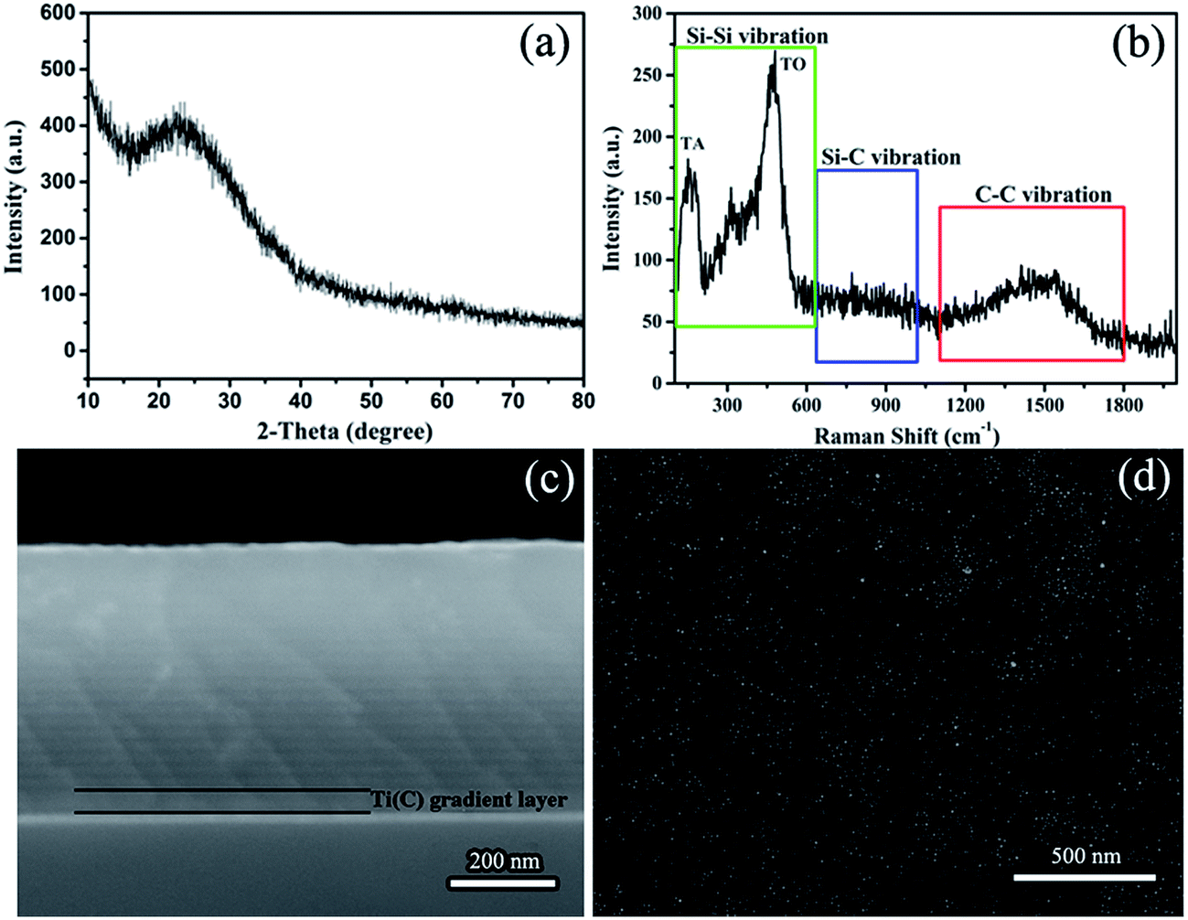 | ||
| Fig. 1 The structure of Si/C multilayer film deposited by sputtering. (a) Raman spectra, (b) XRD pattern, (c) cross-section and (d) the surface SEM image of the multilayer film. | ||
The excellent electrochemical cycling performance can be derived from charge/discharge capacity profiles of Si/C multilayer anodes as showed in Fig. 2a. From the data of Fig. 2b and c, we can observed that the initial discharge and charge specific capacity of sample A are 2940 mA h g−1 and 2800 mA h g−1, respectively. The calculated initial coulomb efficiency (CE) is about 95%. The retention specific capacity is about 2300 mA h g−1 and renders ∼78% of reversible capacity after 200 cycles. The initial discharge and charge specific capacity of sample B are 2640 mA h g−1 and 2560 mA h g−1, respectively. The calculated initial coulomb efficiency is about 97%. The retention specific capacity is also about 2300 mA h g−1 with 87% of capacity retention after 200 cycles. The specific capacity of sample A is higher than that of sample B, which is because of more silicon in sample A. But the capacity degradation of sample A is obvious after 160 cycles.
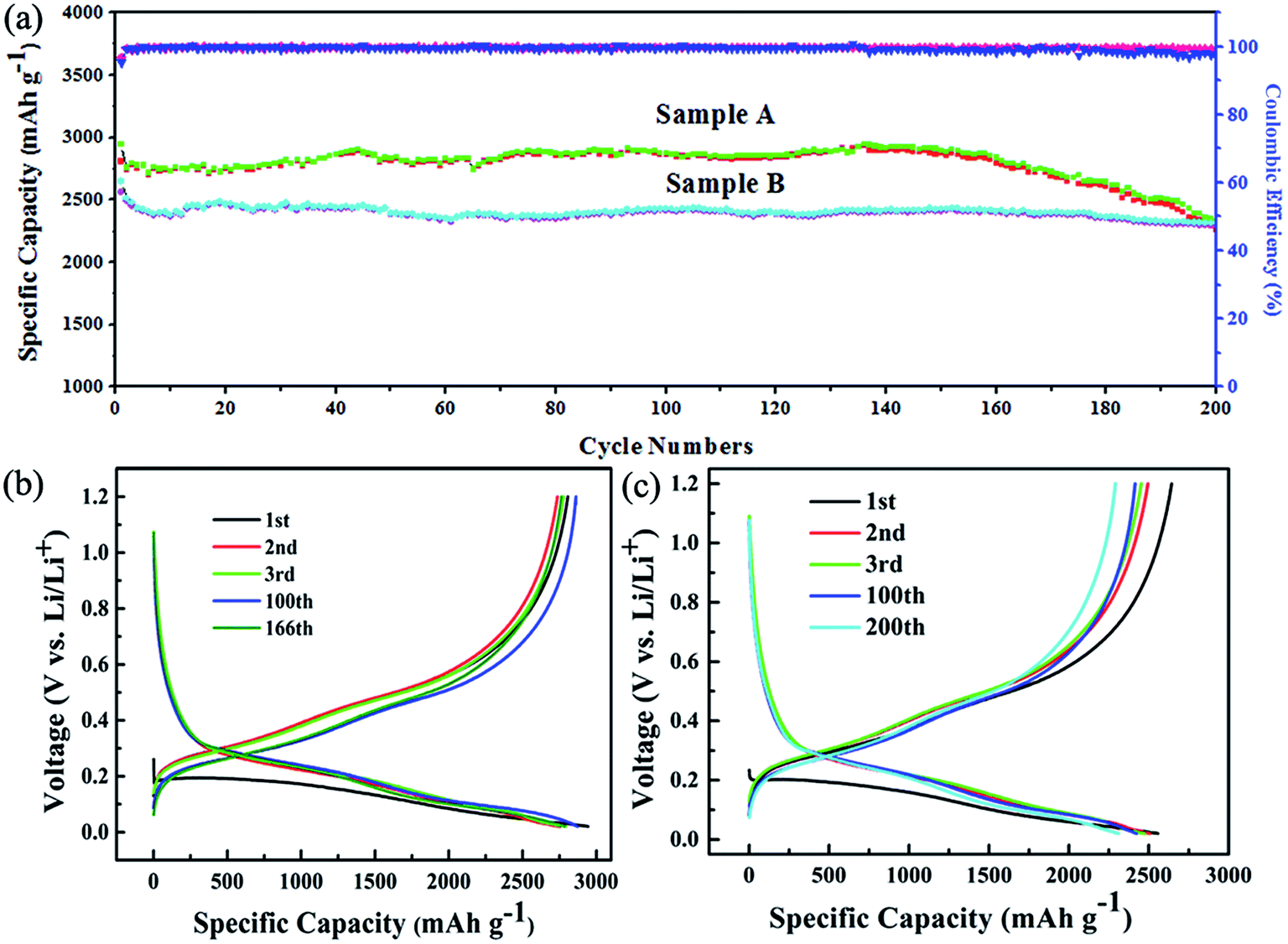 | ||
| Fig. 2 (a) Charge/discharge capacity profiles and coulomb efficiency of the sample A and B at a current density of 400 mA g−1 with the voltage range of 0.01–1.2 V. (b) Voltage profiles of the 1st, 2nd, 3rd, 100th, and 166th for sample A and (c) voltage profiles of the 1st, 2nd, 3rd, 100th, and 200th for sample B. | ||
Fig. 3 shows the surface morphology of the samples after 200 cycles. The cracking in sample A is more serious than that of sample B, which would be the reason for sample A possessing the smaller initial coulombic efficiency and the retention specific capacity. The SEM surface morphology after 200 cycling of a 300 nm silicon film deposited on Cu foils that did not polish with sandpaper and have no Ti(C) gradient intermediate layer is showed in Fig. 3c. It is fractured and exfoliated. These results should be attributed to the three reasons below.
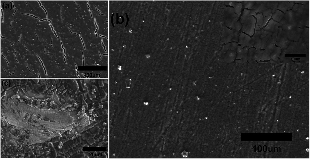 | ||
| Fig. 3 The SEM surface morphology of sample A (a), B (b) and pure silicon film anode (c) after 200 cycles. The inset in (b) corresponds to the high magnification image of sample B after 200 cycles. | ||
Firstly, the carbon layers inserted between silicon layers can effectively relieve stress concentration during the lithiation/delithiation of silicon. According to the literature,20,21,26,30,33–35 thinner amorphous C buffer layer can maintain microstructural stability of the a-C/Si based anode through releasing stresses induced by volume expansion during the charge/discharge cycles. One-dimensional model predicts that below a critical silicon particle size the further fracture will not occur.26 For a-Si film, it is about 100 nm even under repeated cycling.36,37 In our experiment, the single silicon layer is less than 20 nm. Based on mentioned above, we show a stress, constraint and volume expansion schematic illustration in Fig. 4. Due to the homogeneity and thin silicon layer deposited by sputtering, transverse stress parallel to the film surface is constrained by the carbon layer and is adjusted to the longitudinal direction during lithiation of silicon in Si/C multilayer film. That results in the expanding of silicon along the vertical direction to film surface mainly.
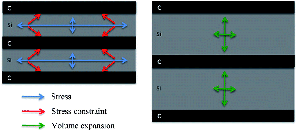 | ||
| Fig. 4 The stress, constraint and volume expansion schematic illustration. | ||
Secondly, the Ti(C) gradient intermediate layer between Cu foil and Si/C film and relatively well matching between silicon and carbon at their interfaces ensure a good combination between the layers. The furrow shaped surface of copper foil also devote to the suppressing of Si/C multilayer films anode fracture.
Thirdly, carbon coated on Si/C multilayer surface as a protective layer can efficiently cut off the direct contact between Si and electrolyte38 and form a relatively stable solid electrolyte interphase (SEI) film,10,39–41 thereby improving the electrochemical performance.
Cyclic voltammograms (CVs) depicted in Fig. 5 show that the first cycle of CV profiles is quite different from the subsequent cycles. A broad peak around 1.0 V corresponding to the formation of SEI layer6,41–44 does not appear in our experiment, suggesting limited SEI layer formed on the sputtering film with a 20 nm carbon protective layer. This's why the Si/C multilayer films deposited by sputtering method have higher initial CE and retention capacities than the reported.10,42,45,46 When the scan proceeds, there is a sharp cathodic peak arising at a low potential of below 0.3 V for sample A and 0.2 V for sample B respectively, which is related to the lithiation and amorphization of silicon.4,41,42,44,47–50 One broad oxidation peak appear correspondingly at 0.56 V for sample A and 0.58 V for sample B on the reversed scan, corresponding to Li extraction from the Si/C multilayer films.4,41,42,48–51 In our experiment, the only one broad anodic peak in the first CV curves indicates the cathodic peak below 0.3 V for sample A and 0.2 V for sample B should be corresponding to one process (based on the capacity as showed in Fig. 2, we believe the silicon converted into an amorphous LixSi (x < 3.75), which is not the full electrochemical room-temperature lithiation of Si (i.e., Li3.75Si)).41
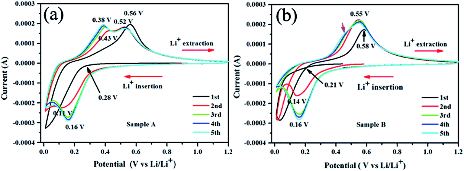 | ||
| Fig. 5 The first five cyclic voltammetry (CV) curves for the Si/C multilayer film electrodes (sample A and B) at a scanning rate of 0.1 mV s−1 within a voltage range of 0.01–1.2 V versus Li/Li+. | ||
During the second cathodic sweep, a new reduction peak was observed at 0.11 V for sample A and 0.15 V for sample B, respectively, which are most likely related to another alloying reaction of Li+ with silicon. In the case of the ongoing cycles, there is no substantial change in the peak potentials and curve shape.
As showed in Fig. 5, the oxidation and reduction potential is slightly different for sample A and sample B, this is because of the different silicon thickness in sample A and B. In the redox process of silicon, carbon layer influences the redox potential. We can derive from the electronic binding energy as showed in Fig. 6. On silicon side at the Si/C interfaces, the binding energy of C1s electron is lower than that on carbon side and the carbon content (the intensity of C1s peak) has increase from silicon side to carbon side. Meanwhile, on silicon side at the Si/C interfaces, the binding energy of Si2p electron is lower than that on carbon side and the silicon content (the intensity of Si2p peak) has decrease from silicon side to carbon side. Which is coincident with the reported.52 The binding energy of Si2p and C1s electrons are changed periodically and influenced each other. These results show that the carbon and silicon diffused into each other at the Si/C interfaces and the interfaces of Si/C are not sharp.
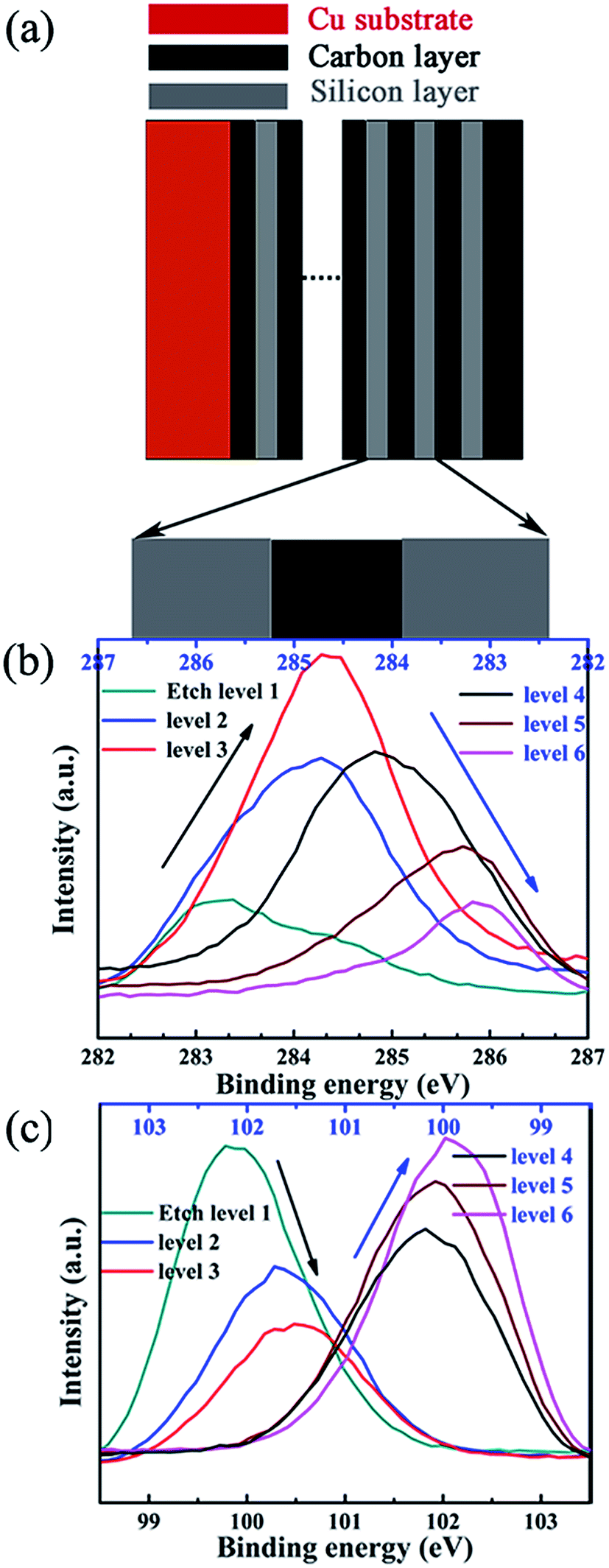 | ||
| Fig. 6 The schematic illustration of Si/C multilayer film (a), the binding energy changing of C1s (b) and Si2p electrons (c) in Si/C multilayer film deposited by sputtering method. | ||
The electrochemical impedance spectroscopy (EIS) was used to further study the interfacial characteristic, charge transfer and ion diffusion kinetics of the Si/C multilayer thin film electrodes. The Nyquist plots for Si/C multilayer thin film electrodes consists of a straight line in the low frequency region and a depressed semicircle in the high frequency region as showed in Fig. 7. The depressed semicircle in the high-to-medium frequency region corresponds to the combined impedance of the SEI film (Rsei), contact interface (Rint) (among the current collector and active material, among silicon layer and carbon layer) and the information about charge-transfer resistance (Rct).53–56 The inclined line in the low frequency region corresponds to the Warburg impedance (Zw) during the solid-state lithium-diffusion process in the electrode materials.57–59
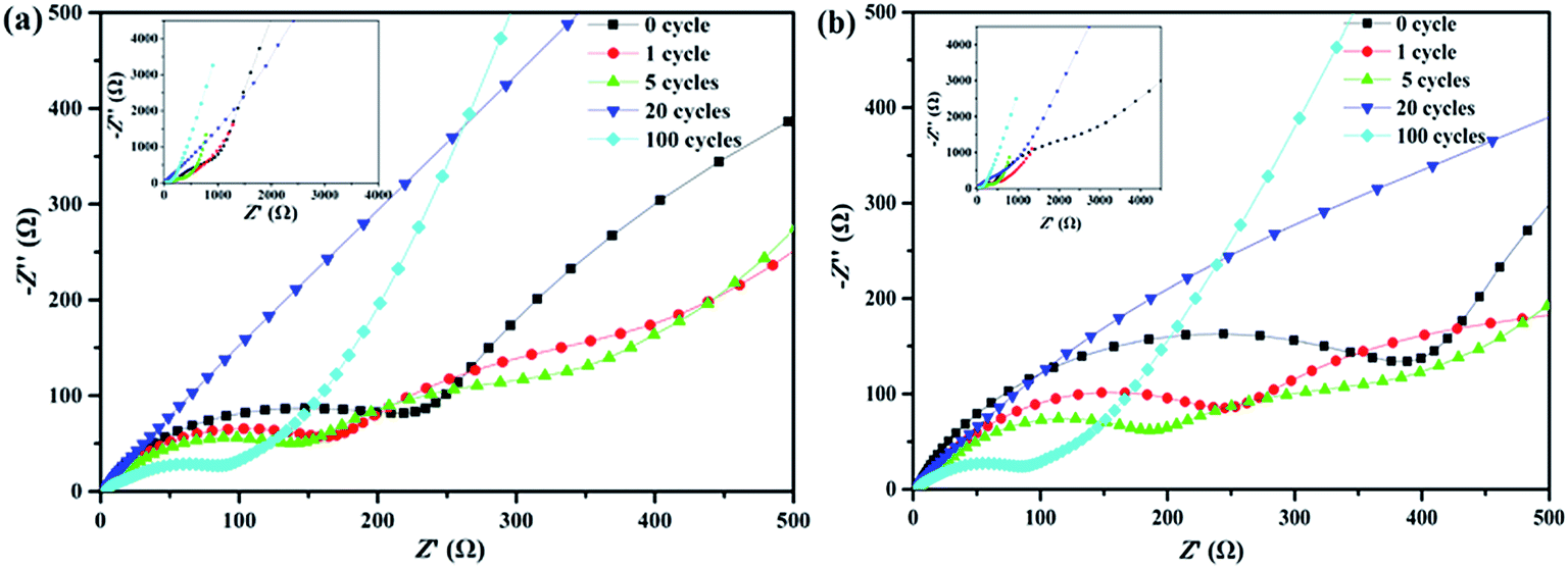 | ||
| Fig. 7 Nyquist plots of the sample A (a) and B (b) in the high-frequency range after different cycles. Insets are the plots from low-frequency to high-frequency. | ||
It is noted that the depressed semicircle undergo a gradually decreasing process in the first 20th cycles for both half-cells. Afterwards, both of the resistances increase to some degree (Fig. 7a and b). This phenomenon might be explained as follows:
Before the cycling, the Si/C multilayer films have relatively high interfacial and charge transfer resistance (Rint + Rct), but low Rsei because of limited SEI film formed as described before. In the earlier dozens of cycles, the films maintained completely and did not crack. Thus the Rsei formed on carbon layer can maintain constant60 and the Rint + Rct decrease with the lithiation/delithiation of silicon and the interface blurring between silicon layer and carbon layer. The depressed semicircle became smaller and smaller. After 20th cycles or so, the films began to break. The electrolyte invaded the film along crack and contacted with silicon directly. More and more SEI films formed and the Rsei increased. The depressed semicircle radius increased to a certain extent after 100th cycling as showed in Fig. 7.
4. Conclusions
In this work, we design and synthesis the multilayer film Si/C nano-structure by magnetron sputtering method. Using carbon layer as silicon volume expansion buffer, suppressing the film cracking during lithiation/delithiation and separating the silicon from organic electrolyte, the Si (15 nm)/C (5 nm) multilayer film anode shows excellent electrochemical properties. The initial discharge and charge specific capacity of which are 2640 mA h g−1 and 2560 mA h g−1 with initial coulomb efficiency of ∼97%. The retention specific capacity is about 2300 mA h g−1 and renders ∼87% of capacity retention after 200 cycles. The carbon and silicon affects the electron status each other. The binding energy of silicon and carbon are changed periodically and reflected in redox potential difference in sample A and B. Although the Si (15 nm)/C (5 nm) multilayer film anode shows better cycling properties, the interfacial and charge transfer resistance (Rint + Rct) is higher than Si (20 nm)/C (5 nm) multilayer film anode because of more Si/C interface in Si (15 nm)/C (5 nm) multilayer film.Conflicts of interest
There are no conflicts to declare.Acknowledgements
This work was supported by the Fundamental Research Funds for the Central Universities (lzujbky-2016-114, lzujbky-2016-120) and the Open Project of Key Laboratory for Magnetism and Magnetic Materials of the Ministry of Education, Lanzhou University under award number LZUMMM2016012.References
- J. M. Tarascon and M. Armand, Issues and challenges facing rechargeable lithium batteries[J], Nature, 2001, 414(6861), 359 CrossRef CAS PubMed.
- M. Armand and J. M. Tarascon, Building better batteries[J], Nature, 2008, 451(7179), 652 CrossRef CAS PubMed.
- U. Kasavajjula, C. Wang and A. J. Appleby, J. Power Sources, 2007, 163, 1003–1039 CrossRef CAS.
- M. N. Obrovac and L. Christensen, Electrochem. Solid-State Lett., 2004, 7, A93 CrossRef CAS.
- W. Wang, M. K. Datta and P. N. Kumta, J. Mater. Chem., 2007, 17, 3229 RSC.
- G. C. L. a. R. A. H. B. A. Boukamp, J. Electrochem. Soc., 1981, 128, 4 CrossRef.
- N. Y. K. Amezawa, Y. Tomii and Y. Lto, J. Electrochem. Soc., 1998, 145, 8 CrossRef.
- M. W.-M. a. R. A. H. W. J. Weydanz, J. Power Sources, 1999, 81–82, 5 Search PubMed.
- W.-J. Zhang, J. Power Sources, 2011, 196, 13–24 CrossRef CAS.
- H. Wu, G. Chan, J. W. Choi, I. Ryu, Y. Yao, M. T. McDowell, S. W. Lee, A. Jackson, Y. Yang, L. Hu and Y. Cui, Nat. Nanotechnol., 2012, 7, 310–315 CrossRef CAS PubMed.
- X. Zhao, C. M. Hayner, M. C. Kung and H. H. Kung, Adv. Energy Mater., 2011, 1, 1079–1084 CrossRef CAS.
- M. Thakur, S. L. Sinsabaugh, M. J. Isaacson, M. S. Wong and S. L. Biswal, Sci. Rep., 2012, 2, 795 CrossRef PubMed.
- B. M. Bang, J.-I. Lee, H. Kim, J. Cho and S. Park, Adv. Energy Mater., 2012, 2, 878–883 CrossRef CAS.
- X.-y. Zhou, J.-j. Tang, J. Yang, J. Xie and L.-l. Ma, Electrochim. Acta, 2013, 87, 663–668 CrossRef CAS.
- X. Chen, K. Gerasopoulos, J. Guo, A. Brown, C. Wang, R. Ghodssi and J. N. Culver, Adv. Funct. Mater., 2011, 21, 380–387 CrossRef CAS.
- X. Ding, X. X. Liu and Y. Huang, et al. Enhanced electrochemical performance promoted by monolayer graphene and void space in silicon composite anode materials [J], Nano Energy, 2016, 27, 647–657 CrossRef CAS.
- M. Ko, S. Chae, S. Jeong, P. Oh and J. Cho, ACS Nano, 2014, 8, 591–8599 CrossRef PubMed.
- T. B. S. Bourderau and D. M. Schleich, J. Power Sources, 1999, 81–82, 4 Search PubMed.
- J. P. Maranchi, A. F. Hepp and P. N. Kumta, Electrochem. Solid-State Lett., 2003, 6, A198 CrossRef CAS.
- J. P. Maranchi, A. F. Hepp, A. G. Evans, N. T. Nuhfer and P. N. Kumta, J. Electrochem. Soc., 2006, 153, A1246 CrossRef CAS.
- L. B. Chen, J. Y. Xie, H. C. Yu and T. H. Wang, J. Appl. Electrochem., 2009, 39, 1157–1162 CrossRef CAS.
- W. Li, R. Yang, X. Wang, T. Wang, J. Zheng and X. Li, J. Power Sources, 2013, 221, 242–246 CrossRef CAS.
- Y. Tong, Z. Xu, C. Liu, G. a. Zhang, J. Wang and Z. G. Wu, J. Power Sources, 2014, 247, 78–83 CrossRef CAS.
- T. Takamura, S. Ohara, M. Uehara, J. Suzuki and K. Sekine, J. Power Sources, 2004, 129, 96–100 CrossRef CAS.
- H. Guo, H. Zhao, C. Yin and W. Qiu, Mater. Sci. Eng. B, 2006, 131, 173–176 CrossRef CAS.
- W. D. N. R. A. Huggins, Ionics, 2000, 6, 7 CrossRef.
- J. Y. Lee, D. T. Ngo and C. J. Park, Ge−Al Multilayer Thin Film as an Anode for Li-ion Batteries[J], J. Korean Ceram. Soc., 2017, 54(3), 249–256 CrossRef CAS.
- S. H. Ng, J. Wang, K. Konstantinov, D. Wexler, J. Chen and H. K. Liu, J. Electrochem. Soc., 2006, 153, A787 CrossRef CAS.
- J.-B. Kim, H.-Y. Lee, K.-S. Lee, S.-H. Lim and S.-M. Lee, Electrochem. Commun., 2003, 5, 544–548 CrossRef CAS.
- M. K. Datta, J. Maranchi, S. J. Chung, R. Epur, K. Kadakia, P. Jampani and P. N. Kumta, Electrochim. Acta, 2011, 56, 4717–4723 CrossRef CAS.
- J. G. H. R. Tsu and F. H. Pollak, J. Non-Cryst. Solids, 1984, 66, 6 CrossRef.
- R. L. C. Vink, G. T. Barkema and W. F. van der Weg, Phys. Rev. B, 2001, 63(11), 115210 CrossRef.
- M. Uehara, J. Suzuki, K. Tamura, K. Sekine and T. Takamura, J. Power Sources, 2005, 146, 441–444 CrossRef CAS.
- T. Takamura, M. Uehara, J. Suzuki, K. Sekine and K. Tamura, J. Power Sources, 2006, 158, 1401–1404 CrossRef CAS.
- C. Yu, X. Li, T. Ma, J. Rong, R. Zhang, J. Shaffer, Y. An, Q. Liu, B. Wei and H. Jiang, Adv. Energy Mater., 2012, 2, 68–73 CrossRef CAS.
- A. K. D. Juchuan Li, Y. Li, F. Yang and Y.-T. Cheng, J. Electrochem. Soc., 2011, 158, 6 Search PubMed.
- J. Graetz, C. C. Ahn, R. Yazami and B. Fultz, Electrochem. Solid-State Lett., 2003, 6, A194 CrossRef CAS.
- Y.-N. Zhou, M.-Z. Xue and Z.-W. Fu, J. Power Sources, 2013, 234, 310–332 CrossRef CAS.
- P. Verma, P. Maire and P. Novák, Electrochim. Acta, 2010, 55, 6332–6341 CrossRef CAS.
- M. Yoshio, H. Wang, K. Fukuda, T. Umeno, N. Dimov and Z. Ogumi, J. Electrochem. Soc., 2002, 149, A1598 CrossRef CAS.
- J. Saint, M. Morcrette, D. Larcher, L. Laffont, S. Beattie, J. P. Pérès, D. Talaga, M. Couzi and J. M. Tarascon, Adv. Funct. Mater., 2007, 17, 1765–1774 CrossRef CAS.
- J. Wu, X. Qin, H. Zhang, Y.-B. He, B. Li, L. Ke, W. Lv, H. Du, Q.-H. Yang and F. Kang, Carbon, 2015, 84, 434–443 CrossRef CAS.
- H. Jia, C. Stock, R. Kloepsch, X. He, J. P. Badillo, O. Fromm, B. Vortmann, M. Winter and T. Placke, ACS Appl. Mater. Interfaces, 2015, 7, 1508–1515 CAS.
- J. Z. Xianghong Liu, W. Si, L. Xi, B. Eichler, C. Yan and O. G. Schmidt, ACS Nano, 2015, 9, 7 Search PubMed.
- M. Ko, S. Chae, J. Ma, N. Kim, H.-W. Lee, Y. Cui and J. Cho, Nat. Energy, 2016, 1, 16113 CrossRef CAS.
- I. H. Son, J. Hwan Park, S. Kwon, S. Park, M. H. Rummeli, A. Bachmatiuk, H. J. Song, J. Ku, J. W. Choi, J. M. Choi, S. G. Doo and H. Chang, Nat. Commun., 2015, 6, 7393 CrossRef CAS PubMed.
- C. K. Chan, H. Peng, G. Liu, K. McIlwrath, X. F. Zhang, R. A. Huggins and Y. Cui, Nat. Nanotechnol., 2008, 3, 31–35 CrossRef CAS PubMed.
- J. Li and J. R. Dahn, J. Electrochem. Soc., 2007, 154, A156 CrossRef CAS.
- T. D. Hatchard and J. R. Dahn, J. Electrochem. Soc., 2004, 151, A838 CrossRef CAS.
- Y.-M. Kang, S.-M. Lee, S.-J. Kim, G.-J. Jeong, M.-S. Sung, W.-U. Choi and S.-S. Kim, Electrochem. Commun., 2007, 9, 959–964 CrossRef CAS.
- H. K. a. J. Cho, Nano Lett., 2008, 8, 4 Search PubMed.
- J. Wang, J. Pu, G. Zhang and L. Wang, ACS Appl. Mater. Interfaces, 2013, 5, 5015–5024 CAS.
- W. Wang, Z. Favors, R. Ionescu, R. Ye, H. H. Bay, M. Ozkan and C. S. Ozkan, Sci. Rep., 2015, 5, 8781 CrossRef CAS PubMed.
- J. H. K. Evgenii Barsoukov, J. Hun Kim, C. Oh Yoon and H. Lee, J. Electrochem. Soc., 1998, 145, 7 Search PubMed.
- W. Wang, I. Ruiz, K. Ahmed, H. H. Bay, A. S. George, J. Wang, J. Butler, M. Ozkan and C. S. Ozkan, Small, 2014, 10, 3389–3396 CrossRef CAS PubMed.
- L. Hu, H. Zhong, X. Zheng, Y. Huang, P. Zhang and Q. Chen, Sci. Rep., 2012, 2, 986 CrossRef PubMed.
- J. Wang, J. Chen, K. Konstantinov, L. Zhao, S. H. Ng, G. X. Wang, Z. P. Guo and H. K. Liu, Electrochim. Acta, 2006, 51, 4634–4638 CrossRef CAS.
- Y. Chen, N. Du, H. Zhang and D. Yang, J. Alloys Compd., 2015, 622, 966–972 CrossRef CAS.
- Y. L. a. J. Li, J. Phys. Chem. C, 2008, 112, 4 Search PubMed.
- X. Xu, H. Tan, K. Xi, S. Ding, D. Yu, S. Cheng, G. Yang, X. Peng, A. Fakeeh and R. V. Kumar, Carbon, 2015, 84, 491–499 CrossRef CAS.
| This journal is © The Royal Society of Chemistry 2018 |